
Multi-photon patterning of photoactive o-nitrobenzyl ligands bound to gold surfaces
Brenden A.
Magill
 a,
Xi
Guo
b,
Cheryl L.
Peck
b,
Roberto L.
Reyes
a,
Erich M.
See
a,
Webster L.
Santos
b and
Hans D.
Robinson
*a
a,
Xi
Guo
b,
Cheryl L.
Peck
b,
Roberto L.
Reyes
a,
Erich M.
See
a,
Webster L.
Santos
b and
Hans D.
Robinson
*a
aDepartment of Physics, Virginia Tech, Blacksburg, Virginia 24061, USA
bDepartment of Chemistry, Virginia Tech, Blacksburg, Virginia 24061, USA
First published on 15th October 2018
Abstract
We quantitatively investigate lithographic patterning of a thiol-anchored self-assembled monolayer (SAM) of photocleavable o-nitrobenzyl ligands on gold through a multi-photon absorption process at 1.7 eV (730 nm wavelength). The photocleaving rate increases faster than the square of the incident light intensity, indicating a process more complex than simple two-photon absorption. We tentatively ascribe this observation to two-photon absorption that triggers the formation of a long-lived intermediate aci-nitro species whose decomposition yield is partially determined either by absorption of additional photons or by a local temperature that is elevated by the incident light. At the highest light intensities, thermal processes compete with photoactivation and lead to damage of the SAM. The threshold is high enough that this destructive process can largely be avoided, even while power densities are kept sufficiently large that complete photoactivation takes place on time scales of tens of seconds to a few minutes. This means that this type of ligand can be activated at visible and near infrared wavelengths where plasmonic resonances can easily be engineered in metal nanostructures, even though their single-photon reactivity at these wavelengths is negligible. This will allow selective functionalization of plasmon hotspots, which in addition to high resolution lithographic applications would be of benefit to applications such as Surface Enhanced Raman Spectroscopy and plasmonic photocatalysis as well as directed bottom-up nanoassembly.
1. Introduction
For nanofabrication technologies to fulfil their promise, we need the ability to create precise nanoscale patterns, not only on flat substrates, but also on three-dimensional nanostructures and particles. In particular, so-called patchy particles, where surface properties within well-defined regions on the particles have been modified to allow directional interactions, are predicted to assemble into a wide range of complex structures,1–4 and a great deal of experimental effort has therefore been devoted to create patchy particles in recent years.5–9The conventional way to create such surface patterns is through optical lithography, and this technique is today able to reach the nanoscale, at least on flat substrates. To bring the power of optical lithography to textured nanostructures, we need photosensitive films (or resists) that are very thin and can be deposited conformally on complex structures or on particles. In this paper, we study such a film, a self-assembled monolayer (SAM) that uses thiol anchors to bind to metal surfaces, and contains the well-known photo-sensitive o-nitrobenzyl (oNB) group10–19 that cleaves on photoactivation to release a specific chemical moiety, in our case a primary amine. SAMs containing this ligand have been studied in the past, although the bulk of the work has been done on SiO2 and similar surfaces, using silanes to bond to the surface,10,14,16,17,20–23 with a smaller number of papers concerned with thiol-bound SAMs.11,12,19,24 While oNB is the most heavily studied photocleavable protecting group, a number of other moieties with similar properties are also in use.25
The ligands under study are shown in Scheme 1, along with their dominant photoreaction pathway. The disulfide group anchors the ligand to gold surfaces through gold–sulfur bonds, allowing it to form SAMs on the surface. On absorbing either a single photon with sufficient energy or two photons with the same total energy, the molecule may cleave to reveal a primary amine, which is then available for further modification, or can be used simply as a carrier of positive charge, which is how we use it here.
 | ||
| Scheme 1 Abbreviated scheme of the photouncaging of the ligands 1 and 2 used in this paper. Two IR photons (or one UV photon) activate the o-nitrobenzyl group to reveal a primary amine group. The disulfide on the other end of the ligand can form a dual bond to a metal surface allowing the self-assembly of these ligands into a monolayer on gold and other metals. | ||
The absorption spectrum of 1 in an ethanolic solution is indicated by the red trace in Fig. 1. The absorptivity goes to zero at wavelengths longer than 400 nm, which is reflective of the fact that at least 3.1 eV is required to optically activate the oNB group in 1. In other words, ultraviolet light is required to effect the reaction in Scheme 1 with a single photon. This is a property shared with most photosensitive groups.25 This is to be expected since most bond dissociation energies in organic molecules are in excess of 3 eV.
 | ||
| Fig. 1 (Lower and left scales): Absorptivity versus wavelength for a 50 μM solution of 1 in ethanol (red line). (Upper and right scales): Blue triangles reflect two-photon activation in a SAM at 730 nm, 800 nm, and 900 nm wavelength as explained in section 3.3.3. The insets are surface potential images from sample areas exposed to fs laser pulses at these wavelengths. | ||
This is important in light of the fact that a natural and powerful way to create patchiness in nanoparticles would be to take advantage of plasmon resonances that occur in metal nanostructures. When a plasmon resonance is excited, light is concentrated into nanoscale volumes, known as hotspots, on the particle surface at sharp corners and inside narrow gaps in the structure, providing a natural way to create a nanoscale pattern on the particle surface. In addition, the hotspots are precisely the regions in which reactants and analytes should be brought together to optimally implement plasmon-enhanced catalysis26 and surface-enhanced Raman spectroscopy (SERS),27–29 and it would therefore be very useful if the surface properties at the hotspots could be modified to specifically bind molecules of interest while binding elsewhere is avoided. We have already demonstrated that this is possible in silver nanospheres exposed to ultraviolet light.30
Unfortunately, plasmon resonances in non-spherical nanoparticles made from practical plasmonic materials generally occur at visible or infrared wavelengths, with little or no overlap with the absorption band in photosensitive moieties such as oNB. This problem could, at least in principle, be circumvented by photoactivation through a multi-photon process, where the photoreaction is triggered by the nearly simultaneous absorption of two or more photons, where each photon carries a fraction of the energy required to break the chemical bond. This would make it possible to use light of long wavelengths—well beyond the absorption edge at 400 nm in 1 and similar compounds—to photopattern the SAM.
Such multi-photon processes have the additional advantage that reactions can be restricted to the focal region of a laser beam, so that activation can be targeted to a particular region in a 3D space without causing unwanted reactions to occur elsewhere. Fabrication and patterning based on multi-photon absorption has been used in collagen,31 proposed for and demonstrated for microfabrication of polymers for optical data storage,32–34 and used to fabricate objects with feature sizes down to 65 nm.35 A variety of materials have been developed for these and similar applications, including positive33 and negative36 tone polymer systems, inorganic–organic hybrid materials,37 and metal nanocomposites.38 Part of the purpose of this paper is to help establish photoreactive SAMs as a viable multi-photon-sensitive material. As outlined in the Conclusions section, this may allow for optical lithography with resolution as high as 10 nm.
For this reason, we are investigating two different photosensitive oNB ligands: 1, which has a standard photosensitive moiety, and which we have investigated previously,24,39 and 2, which contains an extended conjugated system (in the form of a 4′-methoxy-4-nitrobiphenyl moiety) that confers a particularly large cross section for two-photon absorption. Compounds similar to 1 are known to have a relatively modest cross section for two-photon absorption, on the order of 0.03 G.M.,40,41 compared to as much as 3 G.M. or more for species with the same photosensitive moiety as 2.42 Accordingly, for a given light intensity, it should be possible to perform nonlinear lithography with as much as 100 times greater speed with 2 compared to 1.
Álvarez et al. have previously demonstrated that ultrafast laser pulses at visible wavelengths can cause photoactivation in oNB groups on quartz,21 as have we on gold.39 However, it is not fully established that the activation mechanism in this prior work was optical. This is because oNB ligands are also subject to thermolysis at moderate temperatures,43 and the requirement of simultaneous absorption of more than one photon makes the efficiency of the multi-photon process quite low unless peak light intensities are very high, on the order of GW cm−2, usually furnished by ultrafast laser pulses on a femtosecond timescale. Such pulses can when focused easily raise local temperatures above the thermal activation temperature. This is a particular issue when absorbing materials are present. In our case, experiments are performed on a gold film that absorbs a few percent of the incoming light, converting it into local heating in the span of a few picoseconds.44 This means that in order to use plasmonic hotspots on metal nanostructures the way we have outlined above, thermal damage and thermal activation of surface bound ligands due must be kept to a minimum, or the desired patterning will not occur.
In this paper, we demonstrate that photoactivation due to multi-photon absorption in photosensitive SAMs on gold surfaces is indeed possible and can be dominant over thermal processes, at least when the average light intensity is sufficiently low—on the order of 5 MW cm−2 or less. At higher intensities, optical activation gradually gives way to damage to the SAM. We show that this damage is consistent with a thermal process rather than with ablation or similar rapid onset phenomena. The threshold for thermal damage is also high enough that full optical activation can be accomplished on time scales of tens of seconds to minutes, which makes multi-photon activation in our ligands practical for applications such as photolithography.
In the experiments presented here, we measured the change in surface potential of SAMs activated with near infrared light from an ultra-fast laser with femtosecond pulse duration, measured as a function of both exposure time and the intensity of the incident light. The surface potential of the SAMs activated in this way increases with time and intensity until it reaches a maximum, and then decreases with further irradiation. We identify this decrease as the consequence of damage to the SAM, likely in the form of breaking the thiol bonds that bind the ligand to the Au surface.
Before the onset of damage, we also observe, at low degrees of ligand activation, that the surface potential change is proportional to the exposure time, but supralinear in the light intensity, which is indicative of a multi-photon process.
2. Experimental
2.1 Organic synthesis
The synthesis of 1 was performed using a method described in detail elsewhere.24 Ligand 2 was synthesized as follows: a 10 mL round bottom flask was charged with lipoic acid (86 mg, 0.418 mmol, 1.2 equiv.) and purged with nitrogen. Toluene (2 mL) was added to dissolve the solid. Triethylamine (0.073 mL, 0.522 mmol, 1.5 equiv.) and diphenylphosphoryl azide (dppa) (0.083 mL, 0.3837 mmol, 1.1 equiv.) were added carefully, and the reaction mixture was stirred for 3 h at room temperature. 2-(4′-Methoxy-4-nitro-[1,1′-biphenyl]-3-yl)propan-1-ol (100 mg, 0.348 mmol, 1 equiv., synthesized according to a procedure reported by Bühler et al.45) was added later, and the mixture was heated to 80 °C and stirred for 3 days. The resulting solution was cooled to room temperature and then concentrated in vacuo. The crude mixture was purified by flash column chromatography on silica gel twice to give the desired product (29 mg, 17%).2.2 SAM deposition
Substrates, either silicon or glass, were cleaned by immersion into freshly made piranha solution (3 parts by volume concentrated H2SO4![[thin space (1/6-em)]](https://www.rsc.org/images/entities/char_2009.gif) :1 part 30% H2O2) for 10 minutes, and thoroughly rinsed with DI water. The substrates were then metallized by depositing a 5 nm film of Ti followed by 500 nm of Au through electron beam evaporation. After metallization, the substrates were cleaned a second time for 15 minutes in a fresh piranha solution, and then washed with DI water. To remove oxidation on the Au surface caused by the piranha clean step, the substrates were then soaked in ethanol for 10 minutes. The clean substrates were placed in an ethanol solution containing an abundance (≥0.5 mM) of 1 or 2, and incubated under argon for 16 hours. Upon removal from the solution, the substrates were rapidly rinsed with ethanol and dried with a stream of dry nitrogen gas. The samples were then patterned as soon as practical—in all instances within one day.
:1 part 30% H2O2) for 10 minutes, and thoroughly rinsed with DI water. The substrates were then metallized by depositing a 5 nm film of Ti followed by 500 nm of Au through electron beam evaporation. After metallization, the substrates were cleaned a second time for 15 minutes in a fresh piranha solution, and then washed with DI water. To remove oxidation on the Au surface caused by the piranha clean step, the substrates were then soaked in ethanol for 10 minutes. The clean substrates were placed in an ethanol solution containing an abundance (≥0.5 mM) of 1 or 2, and incubated under argon for 16 hours. Upon removal from the solution, the substrates were rapidly rinsed with ethanol and dried with a stream of dry nitrogen gas. The samples were then patterned as soon as practical—in all instances within one day.
2.3 Patterning
Non-linear patterning of our samples was done through a Zeiss LSM 510 laser scanning microscope connected to a Chameleon Ultra II Ti:Sapph laser with a pulse width of 140 fs and a repetition rate of 80 MHz as the light source. The laser was focused onto the SAM through a 20× objective with the sample in air. To image or pattern the sample the LSM scanned the focal region of the laser beam in a raster pattern with deflection speeds ranging from 6.1 mm s−1 to 610 mm s−1.2.4 Kelvin probe force microscopy
The change in surface potential of our samples was measured with a Bruker Dimension Icon atomic force microscope (AFM) using frequency modulated Kelvin probe force microscopy (KP-FM) that allows the sample surface potential to be measured as a function of position. Bruker SCM-PIT platinum iridium coated tips were used for KP-FM measurements and they were cleaned in an ozone cleaner for 30 minutes after every three to five imaging sessions to maintain a stable surface potential at the tip. The AFM is located in the room adjacent to the LSM 510, and KP-FM measurements on the samples were performed within no more than two hours following laser exposure. This minimizes the chances that newly revealed amine groups on the sample pick up contaminants from the atmosphere, something they are otherwise prone to do. These precautions resulted in highly repeatable modulations in surface potential, which was essential to the quantitative analysis of the data detailed below. We should note that KP-FM naturally has a lower resolution than standard AFM, because it relies on an electrostatic interaction between the surface and the tip. Since the whole tip is conductive, a wider region on the sample will inevitably be sampled than in imaging modes relying on physical contact between the tip apex and sample, resulting in a spatial resolution of no more than a few hundred nm.2.5 Nanosphere adsorption
The substrates were immersed for at least one hour in a solution of negatively charged citrate-terminated Au nanoparticles, synthesized as prescribed by Frens.46 After immersion, the samples were twice briefly sonicated in nanopure water, rinsing the surface with more water after each sonication to remove any unattached nanoparticles.3. Results and discussion
3.1 Surface potential measurement
As can be seen in Scheme 1, the photoreaction in 1 results in an exposed primary amine that acquires a positive charge at sufficiently low ambient pH. This means that in a SAM on gold that is composed of 1, changes in surface potential can be used as a measure of the state of the film. More specifically, we expect that the greater the degree of photoreaction in a SAM, the more positive the surface potential. For this reason, our primary tool for characterizing the film is atomic force microscopy (AFM), operating in Kelvin Probe Force Microscopy (KP-FM) mode, which can measure relative changes in the surface potential of an electrically conducting sample as a function of position across the substrate.The potential measured by KP-FM is due to the interaction between the AFM tip and the sample surface. Therefore, the state of the tip is as important as the state of the sample. Specifically, a small amount of otherwise inconsequential contamination of an AFM tip can significantly change the measured potential, which will then vary between measurements and from tip to tip in uncontrolled ways. As a result, the absolute potential readings in KP-FM are of little value, but with careful and consistent preparation of both sample and tip as described above, the potential contrast between exposed and unexposed regions of the SAM can be made repeatable and used as a semi-quantitative indicator of the surface state.
A priori, we might expect cleaving of a ligand 1 SAM to result in a positive shift of the surface potential, since cleaving exposes a primary amine, which is wont to carry a positive charge. Fig. 2(a) shows an example of the surface potential measured across a pattern exposed with focused femtosecond pulses at 730 nm in the shape of a “VT” logo. Within the exposed area, the potential is relatively constant but more positive than in the unexposed area. As we will see, this corresponds, as far as we can tell, to a nearly fully photoreacted SAM. Fig. 2(b) shows a similar scan, but in this case the substrate was exposed with 405 nm ultraviolet light through a photolithography mask using a mask aligner. The mask pattern is that of a grating on a 10 μm pitch. The total shift from unexposed to exposed regions is quite small in this case, but is still positive. The smaller shift is likely due either to contamination of the SAM during the time it was transferred from the cleanroom to the AFM facility, which are in different buildings, or to incomplete exposure of the SAM, as 400 nm is at the edge of its photosensitivity. To verify the size of the potential shift in a completely photoreacted SAM, we prepared two identical SAM-coated samples, and exposed one of them to 365 nm light in a Fisher Scientific FB-UVXL-1000 ultraviolet cross linker at a total dose of 1 J cm−2, which we know causes complete photoreaction in the SAM.24 We measured the surface potential on both samples in multiple location with KP-FM, and found the potential to be consistently higher in the UV exposed sample by an average of 84 mV. This supports the notion that the SAMs in Fig. 2 are altered in the same way by the red light femtosecond pulses as by UV light exposure, consistent with multi-photon-induced photocleavage.
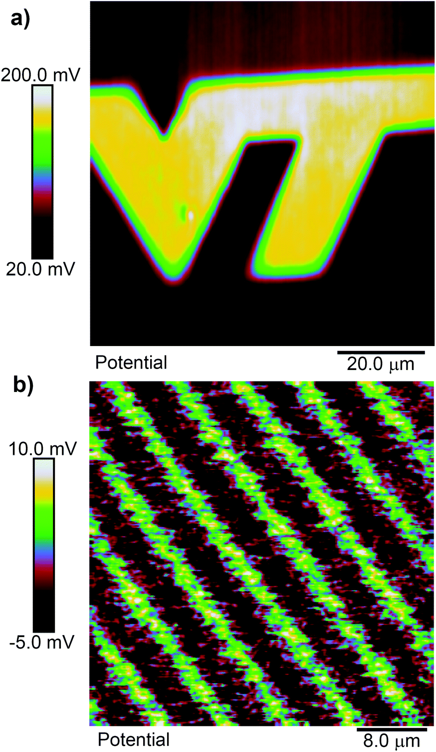 | ||
| Fig. 2 KP-AFM measurement of ligand 1 SAMs activated with (a) fs pulsed light at 730 nm wavelength scanned across the surface, and (b) 365 nm light through an optical mask patterned with a grating composed of 5 μm wide stripes on a 10 μm pitch. | ||
3.2 Multi-photon patterning
To quantify the effect of the ultrafast light pulses, we varied the exposure time and intensity in a systematic fashion. Generally, the surface of our SAM-coated gold samples was exposed in grids consisting of 5 × 2 μm rectangular pads, where light intensity and total exposure time were varied along the vertical and horizontal axes of the grid respectively. KP-FM and AFM tapping mode topography scans over such a grid are shown in Fig. 3.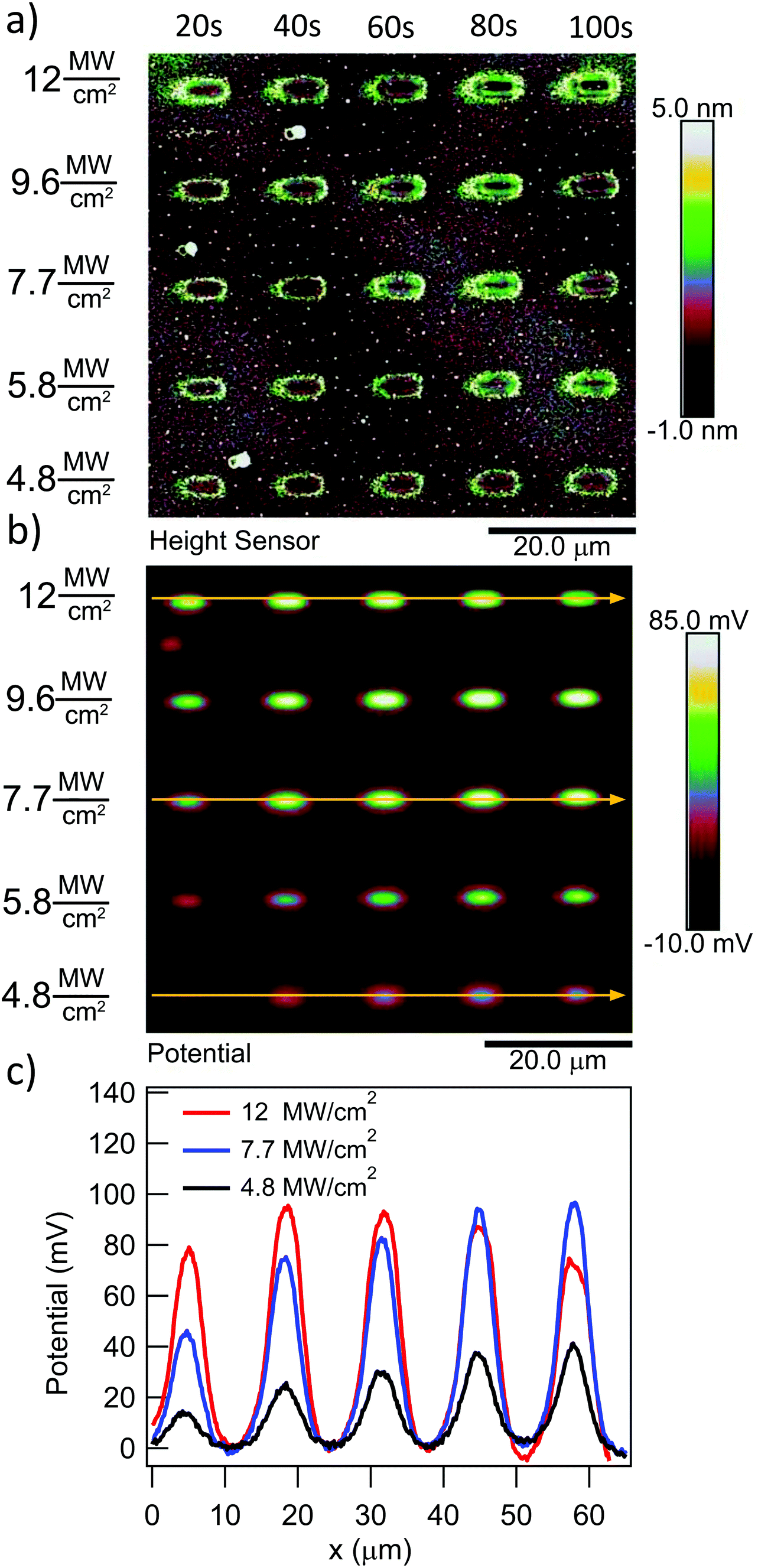 | ||
| Fig. 3 AFM measurement of a SAM of ligand 1 patterned with 730 nm photons. Each 5 × 2 μm rectangular pad was dosed with incident average light intensities and effective exposure times as shown along the left and top sides of the panels. Panel (a) displays the topography of the surface collected in tapping mode AFM, and panel (b) the change in surface potential as measured with Kelvin probe force microscopy. Panel (c) graphs the change in potential taken along the yellow lines in (b). | ||
The KP-FM data (Fig. 3(b)) exhibit the expected increase in surface potential within the exposed pads, where the potential is generally greater the higher the laser power and the longer the exposure time. Except, that is, at the highest power densities, where we believe SAM damage is beginning to set in. The exposed pads are set on a grid with a 15 μm pitch, which is sufficiently widely spaced that neighboring pads do not significantly affect each other, and that a well-defined background potential can be found in the neighborhood of each exposed pad.
To extract a quantitative change in surface potential ΔVS for each of the pads, the KP-FM data was first flattened with respect to the background to remove small gradients in the background potential that are a characteristic of all images collected in this mode. Horizontal line cuts, such as the traces in Fig. 3(c), were then taken through the middle of each row of rectangles. The peak potential from each pad was used as the ΔVS for the corresponding intensity and exposure time.
The surface topography in and around the exposed pad, shown in Fig. 3(a), vary in a characteristic manner. Each pad is surrounded by a raised border about 1 nm in height. The elevation inside the pad is rather similar to the outside, but the topography is significantly smoother on the inside, as can be seen in Fig. 4, with the rms roughness measured by the AFM equal to about 0.32 nm inside the exposed pad and 0.39 nm outside. The raised border is likely the result of oNB leaving groups accumulating on the periphery of the exposed region, as the ligands inside it are cleaved and the leaving groups mainly settle where they are not disturbed by heating from the scanning laser beam. It is worth noting that the elevation inside the pad is not appreciably lower than outside, even though the leaving group is about a third of the length of ligand 1, and should correspond to a height difference of about 1 nm in a close-packed SAM. This may at least in part be explained by a resettlement of leaving groups inside the pad, but the observation is also consistent with a SAM that is not close-packed, with ligands to a large extent lying down on the substrate or across each other rather than being oriented normal to the surface in a well-ordered brush-like structure. This morphology is typical of SAMs of intermediate density.47 When the SAM is photocleaved, the bulky leaving group is removed, leaving behind a slender alkane chain. However, since both the cleaved and uncleaved ligands are mostly lying down, this results in a reduction in roughness rather than a significant change in surface elevation. The effect of the exposure is perhaps the clearest in the phase image, shown in the middle panel of Fig. 4. The AFM phase lag is 1.0° smaller inside the pad than outside, which means that the AFM tip is dampened less inside the pad, consistent with less soft and potentially sticky organic material being present on the surface within the pad than outside it.
 | ||
| Fig. 4 Close-up of the AFM topography (top panel) and phase (middle panel) of a pad patterned at an intensity of 9.6 MW cm−2 with an exposure time of 40 s. The plot in the lower panel show the height measured along the yellow dotted line in the upper panel. A 1 nm tall raised border can be observed in the topography along the edge of the exposed rectangle. The rms roughness of the topography was 0.32 nm inside the exposed pad (square A), and 0.39 nm outside it (square B). The difference in phase between A and B is −1.0°. | ||
The degree of photoreaction seen in the SAM is determined by exposure time (varied along the horizontal direction of the grid), and the light intensity (varied along the vertical direction). The focused laser beam sweeps out a raster across the surface, which means that the effective exposure time tE in Fig. 3 is given by
 | (1) |
The average laser power used during the exposures is relatively modest, on the order of tens of mW, as measured at the entrance aperture of the microscope objective. On the other hand, the beam is fairly tightly focused, using a 20× objective with a numerical aperture of 0.8. Since the laser spot at the rear aperture of the objective is about 4 mm in diameter, this results in a spot size d of about 0.92 μm at 730 nm, which leads to maximum average intensities at the focus in the range of MW cm−2 as indicated in Fig. 3, where the values are calculated assuming a Gaussian beam profile.
Moreover, the laser outputs pulses that are 140 fs long—which we estimate stretch to about 150 fs by dispersion in the microscope optics—at a rate of 80 MHz. This makes for a duty cycle δ of 1.2 × 10⁻⁵. Accordingly, for a laser power of 10 mW, the average light intensity I at the center of the focus is 1.5 MW cm−2, corresponding to a fluence of 0.019 J cm−2 for each pulse. Assuming a sech-squared shaped pulse, the peak light intensity at the focus is then 110 GW cm−2.
At intensities this high, it is reasonable to be concerned about possible damage to the SAM through ablation or a thermal process. The beginning of this is also seen in Fig. 3(b), where the surface potential in the exposed areas increases with light intensity except for at the very highest intensity (average intensities in excess of 12 MW cm−2), where it instead drops, particularly for the longest exposure times. We discuss this damage in more detail in section 3.5 below. It is preceded by sections 3.3 and 3.4, where we analyze light-induced changes in surface potential below the damage threshold, and conclude with a high degree of confidence that the light does indeed cause photocleaving in the SAM due to multi-photon absorption.
3.3 Light-induced photoreactions below the SAM damage threshold
From what we have observed so far, it appears that red light of sufficient intensity is able to cleave 1 and create a positive surface charge, but we cannot yet be completely certain that this is an optical rather than a thermal effect, because oNB groups are known to be subject to thermal decomposition at temperatures as low as 90 °C.43 To verify the origin of the reaction, we will first attempt to fit the surface potential to models consistent with optical and thermal decomposition to determine whether either describes the data well. Second, we will compare the pulsed-light photoreactivity of ligands 1 and 2. 2 has a significantly greater two-photon absorption cross section than 1, and should thus cleave much faster and with lower light intensity, if the cleavage is indeed induced by two-photon absorption. Finally, we will vary the wavelength of the exciting light, increasing it until two-photon absorption is no longer possible in 1, and observe what effect this has on ΔVS in the exposed pads.| ΔVS = Vm[1 − exp(−β·tE)], | (2) |
If the reaction is induced by multi-photon absorption, β should obey:
| β(opt) = ηIn, | (3) |
If the photoreaction is instead due to a thermal effect, β will obey Arrhenius’ equation:
 | (4) |
Here, E is the activation barrier in Joules, kB is Boltzman's constant, T0 is the local temperature just before the laser scans across the area, and α is a constant that depends on the optical absorption of the substrate and the thermal conduction away from the focus, so that αI = ΔT, the increase in local temperature during laser illumination. Finally, A incorporates the conventional pre-exponential factor in Arrhenius’ equation, but also takes into account the spatial and temporal variations in ΔT during illumination.
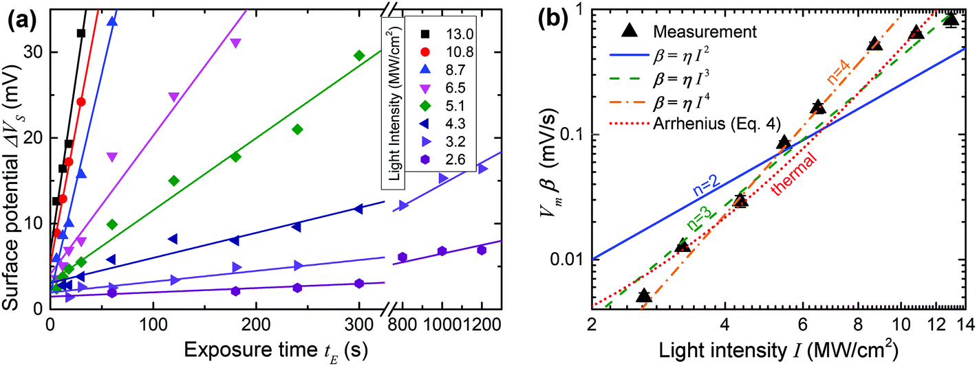
If ΔVS is small compared to Vm, the linear approximation Vm(1 − eβt) ≈ Vmβ·t holds, and the number of free parameters in the models is reduced by one, so that the fit is more reliable. In addition, the effect of thermal damage on the data is also likely to be smaller in this regime. For these reasons, we will fit our data to the models while restricting ourselves to ΔVs < 35 mV, far enough from saturation (which occurs at Vs ≈ 80 mV) that the linear approximation is reasonable.
Fig. 5(a) plots ΔVSvs. time t for 8 different values of I with straight line fits for all potentials up to 35 mV. All the fits are of high quality over a wide range of t values (between 10 s and 1200 s), consistent with the expected linear time dependence away from saturation. This strongly supports the notion that ΔVS is in fact nearly proportional to the fraction of reacted molecules in the SAM, at least for modest values of ΔVS, and a posteriori justifies our analysis.
 | ||
| Fig. 5 (a) Surface potential of exposed pads vs. exposure time for several different laser intensities on a sample conjugated with 1. Each intensity is fit to a straight line, taken to have slope Vm·β. (b) Plot of the slopes extracted in (a) vs. laser light intensity at the sample. The data is fit to a thermal model for activation (dotted red line) and multi-photon activation models involving two photons (solid blue line), three photons (dashed green line) and four photons (dot-dashed orange line). | ||
We do however need to note that the fits in Fig. 5(a) include a constant offset ranging from +2 mV to +5 mV. This is likely due to a bleed-over effect where adjacent pads on the sample boost each other's surface potential. This occurs because the measured value of the surface potential is a result of the interaction of the entire AFM tip with the whole sample surface, which is dominated by the area immediately below the tip, but also affected by more distant parts of the surface, which causes the offset. The effect is fairly small and more importantly does not disturb the conclusion that ΔVS is a good measure of the photoreaction and the slopes of the fits in Fig. 5(a) provide good relative estimates of β. We can therefore proceed to further analyse the data in an attempt to identify the mechanism behind the photoreaction.
Fig. 5(b) contains a log–log plot of the values of β obtained in Fig. 5(a)vs. incident light intensity I. Least squares fits to the optical (eqn (3)) and thermal (eqn (4)) models are also shown in the figure, in the latter case subject to the constraint that ΔT is no larger than 300 K.48 Somewhat surprisingly, two-photon activation (n = 2) is a poor fit to the data, contrary to observations of non-linear photolysis of oNB compounds in solution, where two-photon activation is a dominant effect.40–42,49–52
Reasonably good fits are obtained both for the three photon case (n = 3) and for the thermal model, and these are the best fits if all the data is taken into account. If the two highest light intensities are discarded as suspect due to the possible onset of damage to the film at high light intensities, an even better fit is obtained with n = 4, corresponding to a four-photon process.
Given the clear evidence for two-photon photolysis for oNB compounds in solution, it is perhaps tempting to conclude from the fits in Fig. 5(b) that thermal activation is likely the dominant process at work here, obscuring the two-photon photoreaction that would otherwise take place. Yet, there are several reasons why we can in fact exclude a purely thermal process as the cause of the trends in Fig. 5(b). First, the thermal fit in the figure corresponds to an activation energy of just 9.1 kcal mol−1 (0.40 eV), and maximum ΔT of 300 K, which is inconsistent with the optical and thermal properties of oNB compounds, as well as calculations.53 Imposing a more realistic activation energy (>30 kcal mol−1, 1.3 eV), leads to a suspiciously small maximum ΔT of about 45 K, and also increases the inflection of the curve, making the fit nearly as poor as in the two-photon case.
 | ||
| Fig. 6 (a) Surface potential data from a gold surface supporting a SAM of 2. The time-averaged intensity and effective exposure times are shown along the top and left sides of the image. (b) Plot of the surface potential of the exposed pads vs. exposure time for different laser intensities, derived from (a). The dashed lines are a guide to the eye. | ||
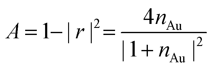 with gold's complex index of refraction nAu as measured by Johnson and Christy,54 we find that 2.7% of the incident light is absorbed by the gold at 730 nm, 2.4% at 800 nm, and 2.0% at 900 nm. In light of the data in Fig. 5, this means that the variations in heat deposited at the different wavelengths is much too low to explain what we see in Fig. 7. On the other hand, Fig. 7 is completely consistent with the absorption spectrum of 1 as plotted in Fig. 1 and a two-photon absorption process as the initial trigger for the decomposition reaction. The linear absorption edge of 1 in ethanol is at 400 nm, which means that we expect the two-photon absorption edge to lie near 800 nm, if the excitation occurs between the same states as in the one-photon case. We therefore expect to see a significantly reduced value of ΔVS when the wavelength is increased from 730 nm to 800 nm, and a zero ΔVS (or negative in the presence of optical damage) at 900 nm, precisely what we observe. To reinforce this point, data from the 40 s exposure series in Fig. 7 is superimposed (as blue triangles) on the absorption spectrum in Fig. 1, where the laser wavelength (top scale, in blue) for each data point is matched with half that wavelength in the absorption spectrum (bottom scale).
 | ||
| Fig. 7 (a) Change in the surface potential of a SAM of ligand 1 after being patterned with 730, 800, and 900 nm light with a time-averaged intensity of 9.6 MW cm−2. (b) Bar chart showing the changes in surface potential ΔVS extracted from the image in (a). | ||
3.4 Mechanism of decomposition
Given the result in the previous section, we must ask why the onset of photocleavage in the 1 SAM is consistent with two-photon absorption when the data in Fig. 5 indicates a higher order process. For a possible explanation, we need to examine the mechanism of the photoreaction in o-nitrobenzyls in more detail.This reaction is rather well understood thanks to a number of studies in recent years (see the review by Klán et al.25 and references therein). The main pathway of the photoreaction is shown in Scheme 2. On photoexcitation of 1, a short-lived (<10 ps) singlet state S1 is formed, which then either undergoes intersystem crossing to the triplet state T1, or decays directly into the (Z)-isomer of the aci-nitro intermediate 4a. The triplet state will form a biradical intermediate BR, which then also decays by hydrogen transfer into one of the isomers of 4.55 The reaction then proceeds by cyclization into the 2,1-benzisoxazoline intermediate 5, which in turn undergoes transformation in two additional steps (not shown), leading to release of the primary amine 3 from the nitroso benzaldehyde leaving group 6. The 4 → 5 cyclization is irreversible,53 but the (Z)-aci-nitro intermediate can return to 1 by transfer of a hydrogen back to the benzylic carbon.53,56
 | ||
| Scheme 2 Photoinitiated decomposition of 1, with several reaction intermediaries. | ||
The rates of the cyclization reaction (k′Z, k′E), the conversion rate kEZ between the (E)- and (Z)-aci-nitro isomers, and of the rate of return to the ground state 1 (kR) all depend sensitively on environmental variables such as solvent, temperature, pH, etc. For example, in protic solvents, kEZ is large as the conversion between isomers can proceed through the conjugate base 4−, leading to a single exponential decay of all isomers of 4 into 1. In non-polar solvents, on the other hand, kEZ is very small, and the (Z) isomer 4a tautomerizes back into 1 at a rate much greater than the (E) isomer 4b.57 Moreover, since both the 4 → 1 and 4 → 5 reaction involve proton transfer, both are subject to acid catalysis—both kR56 and k′58 can be increased by several orders of magnitude by lowering the pH of the reaction.
This reaction has mainly been studied in solution, but there have also been studies in a solid matrix.59 The reaction kinetics in a SAM are much harder to access, and there is therefore understandably no quantitative study of reaction rates under conditions that resemble those of our experiments. Our previous work has shown that the quantum yield of decomposition is similar in such a SAM on gold as in solution, and there is no reason to believe that the mechanism of the reaction should be different in any fundamental way in a SAM, although the reaction rates may differ substantially. The mechanism can be summarized as an optical excitation into a singlet state that within about 2 ns decays into the comparatively long-lived (μs to ms) intermediate 4, which can then either return to the initial state 1, or undergo complete cleavage. In other words, although the reaction involves numerous intermediates, it is functionally a two-step process 1 ⇄ 4 → 3 + 6, where the forward direction of the first step is triggered by absorption of light in 1.
Therefore, the reaction rate β = βaϕd, where βa is the light-induced rate of formation of 4, while ϕd is the yield of the 4 → 3 + 6 decomposition. The data in Fig. 6 indicates that the initial excitation is a two-photon process, which means that βa ∝ I2. Since the slope of the data in Fig. 5(b) clearly is greater than 2, this means that ϕd must be an increasing function of I.
The origin of this I-dependence is likely either optical or thermal. aci-Nitro benzyl moieties have a strong optical absorption peaking near 400 nm.56,58 In addition, they are relatively long-lived (μs to ms range) and therefore likely to absorb photons before decaying. Therefore, if the decomposition reactions of 4 are hastened by two-photon absorption, that would explain the approximate I4 dependence in Fig. 5. Alternatively, the light impinging on the sample does cause heating that affects the reaction rates of 4,60 and likely therefore also ϕd, since it depends on the relative magnitudes of those rates.
In other words, the totality of the data confirms that the cleavage of 1 that we observe in our samples is initiated through two-photon absorption rather than thermal activation over a barrier, even though it is possible that the total quantum yield of decomposition is affected by additional photon absorption events or by the heat that is deposited by the incident light. Since we do not know whether or not the total process involves absorption of more than two photons, we will continue to refer to it as multi-photon photocleavage.
3.5 Exposure above the damage threshold
We now know that we are able to photocleave a SAM made from ligand 1 using multi-photon absorption. The origin of the reduction in ΔVS with increasing I and tE is less clear. In this section, we turn our attention to this issue, first by adsorbing negatively charged nanoparticles onto the exposed areas to assess the damage to the SAM, followed by characterization of how the extent of the damage varies with substrate and with beam scanning rate v. From the results of these tests, we are able to conclude that the damage to the SAM is consistent with a thermally activated process due to an elevated substrate temperature at the beam focus, rather than to direct ablation of the SAM or some other rapid process. | ||
| Fig. 8 SEM micrographs (a) and KP-FM images (b) of three 5 × 2 μm rectangular pads exposed to pulsed 730 nm light for an effective exposure time of 20 s, but with varying intensity as shown. The surface potential ΔVS along the yellow line is shown in (c). The white dots in (a) are negatively charged gold nanospheres adsorbed to the substrate between the KP-FM and SEM measurements, and indicate a photocleaved, but otherwise mostly undamaged film. | ||
At the lower exposure intensities, we can clearly see that particles are adsorbed across the entire area of the pads, with a lower particle density on the less exposed pad, and also with lower densities near the pad edges, where optical intensities were lower due to the Gaussian intensity distribution in the beam. At the highest exposure intensity, which is in the range where ΔVs decreases with increasing time and laser intensity, we instead see the particles mostly adsorbing around the edge of the pad, with few particles in the center, which suggests the SAM has been damaged in this area.
One way to narrow down the range of possibilities is to investigate the timescale of the damage process, which is not clear from the data presented so far, and would vary widely depending on its precise mechanism. If the damage occurs due to a plasma-like excitation in the gold substrate or to direct heating of the SAM, involving mostly or exclusively electronic states, the damage process would be very fast, as the cooling time would be on a sub-picosecond timescale. This would mean that the damage is mainly a function of the fluence of each femtosecond pulse, but would not depend on the pulse separation (about 125 ps) or the dwell time of the laser spot in a given location (μs or longer). In this case, it would not be possible to mitigate the laser damage by improving heat conduction away from the surface or by increasing the laser scanning speed. This also holds if the damage is due to a chemical reaction set off by absorption of a single photon in the ligands. If, on the other hand, the SAM damage is due to high lattice temperature, it occurs on a time scale of at least nanoseconds, which is greater than the separation between laser pulses, and would be subject to mitigation as just mentioned.
To find out which type of mechanism we are dealing with, we varied both heat conduction and laser scanning rate. All the samples discussed up to this point consist of gold evaporated on silicon, and were exposed with the laser focus scanning across the sample at a speed of 610 mm s−1. Silicon has fairly high thermal conductivity (about 100–160 W m−1 K−1, depending on doping). The thermal conductivity of gold is even higher (over 300 W m−1 K−1), but since it is only present as a thin layer, it will have a relatively minor effect on the conduction of heat away from the laser spot. Therefore, the thermal conduction can be significantly lowered by using a substrate made of glass, which has a thermal conductivity on the order of just 1 W m−1 K−1. Fig. 9 plots ΔVs against exposure time at two different laser intensities, and on sample substrates of silicon and glass (indicated by solid and dashed lines, respectively). At the lower intensities (green lines), the behavior of the two substrates is similar, as no significant damage is seen in either case as ΔVs increases roughly linearly with time. At the higher intensity (black lines), ΔVs grows faster initially, but laser damage sets in much earlier. Notably, the damage sets in sooner and is much more complete on the glass substrate, where ΔVs goes back to 0 well before the SAM is fully cleaved, while on the silicon substrate, ΔVs saturates at around 50 mV. This is indicative of some damage even in the silicon case, but clearly much less extensive than for the glass substrate.
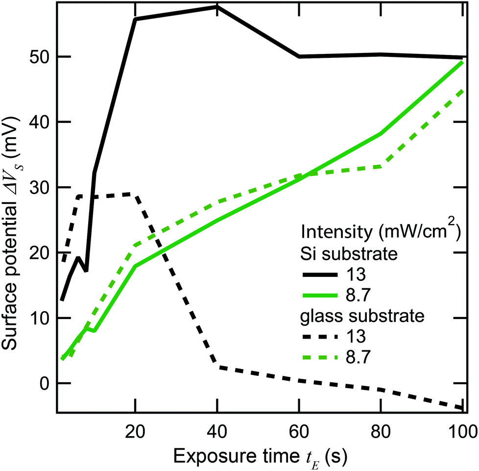 | ||
| Fig. 9 Change in surface potential versus exposure time for two different light intensities on Si and glass substrates. Activation curves for Si are shown as solid lines and for glass as dotted lines. | ||
In our second test, we reduced the laser scanning speed from 610 mm s−1 to 6.1 mm s−1. With a 0.92 μm spot size, this corresponds to an increase in laser dwell time from about 1.5 μs to 150 μs. Fig. 10 shows spatial plots of ΔVs on a gold-coated silicon substrate where the photosensitive SAM was exposed by ultrafast light pulses at 730 nm along vertical stripes, and where the laser was scanned at the fast rate (Fig. 10(a)) and the slow rate (Fig. 10(b)), but where the values of I and tE were the same in both cases. The difference is quite striking. The fast scan gives rise to a positive value of ΔVS of the expected magnitude (>40 mV) indicating that photocleavage of the SAM is taking place without major damage, while the slow scan instead leads to a negative ΔVS consistent with damage to the film. This difference persists over a range of intensities—it is in fact very difficult to obtain a positive change in surface potential when scanning at the slow rate.
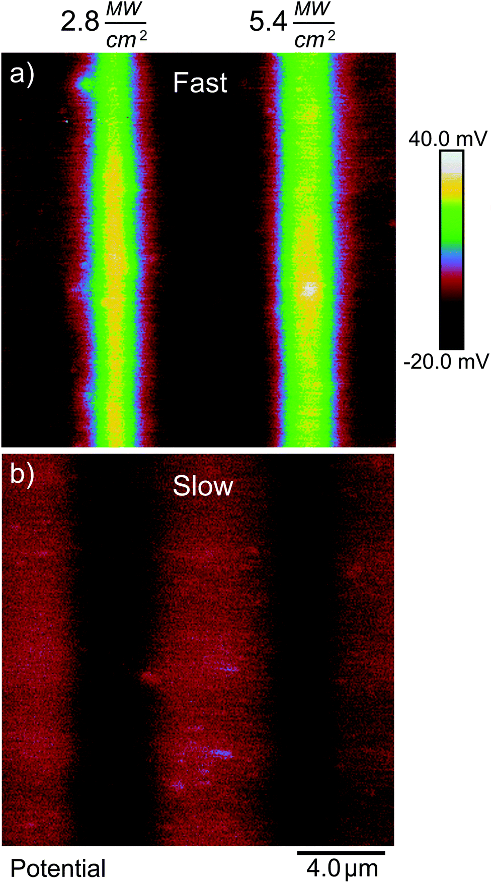 | ||
| Fig. 10 Surface potential changes resulting from lines patterned onto SAMs of 1 with pulsed 730 nm light for the same total effective exposure time but with different laser scan velocities. The laser spot dwell time was approximately 1.5 μs in (a) and 150 μs in (b). | ||
From this we can conclude that the damage to the SAM primarily results from an increase in the local lattice temperature, which in our case takes at least microseconds to reach its maximum value. This does not mean we can exclude smaller contributions from other processes, but lattice temperature is clearly the dominating factor. From this we can conclude that the speed of the photoreaction can be increased further by the use of shorter, more intense pulses, and a higher repetition rate, without risking greater damage to the SAM.
4. Conclusions
In this paper, we have explored multiphoton activation of SAMs composed of bifunctional o-nitrobenzyl ligands on gold surfaces. Our results demonstrate that we can photocleave these ligands with multiphoton absorption of visible, 730 nm, light suitable for plasmonic applications involving metal nanoparticles. In the particular ligands we have used here, this results in the uncaging of a primary amine, which we have shown can be used for adsorption of oppositely charged nanoparticles onto the exposed regions. The amines are also available for further chemical modification, and ligands of this type can be designed to release other moieties, such as carboxyls and alcohols, on photocleaving.At high light intensities, the heat deposited by the light causes damage to the SAM. However, with adequate heat conduction away from the laser focus, and sufficiently short dwell times (on the order of about 1.5 μs) of the laser beam at a given spot on the sample, the threshold of the damage occurs at beam intensities above a few MW cm−2. This leaves us with a large window of laser powers within which patterns tens of μm across can be exposed within minutes without significant damage, even though the peak two-photon absorption cross section of photosensitive ligands such as 1 are generally in the range of 0.01–0.1 G.M.40,41,49–51 oNB ligand specifically designed for cleaving by two-photon absorption can have cross sections in excess of 3 G.M.,42,52 potentially expanding the area that could be patterned in a given time by up to two orders of magnitude.
The fact that we can use visible light to cleave 1 means that it will be possible to use this technique to locally change the surface chemistry at the nanoscale surface plasmon hotspots in metal nanostructures, where the light intensity can be several orders of magnitude higher than in surrounding areas. The patterning is aided by the nonlinear nature of the two-photon absorption process, whose rate is proportional to the square of the light intensity. The selectivity of the photoreaction to the hotspots should therefore equal the square of the hotspot intensity enhancement, or between four and twelve orders of magnitude. As discussed in the Introduction, selective patterning of hotspots could in this way be used to increase the efficiency and sensitivity of plasmon-driven catalytic reactions and SERS analysis.
Another potential application of this technique is directed self-assembly of nanoparticles into well-defined larger constructs. The creation of patches with different surface properties on specific locations on the nanoparticles can, under the right circumstances, lead to ordered self-assembly akin to the way that proteins assembly into more complex structures. Like many other bottom-up assembly techniques, this also has the advantage that it can be performed in suspension rather than on a surface, so that the fabrication process can be efficiently scaled up.
When it comes to conventional lithography on planar surfaces, the combination of multiphoton exposure and the nm thickness of SAMs may allow exceptionally high spatial resolution features to be fabricated. To be more specific, lithography on SAMs with Scanning Nearfield Optical Microsopy (SNOM) relying on linear single-photon absorption has already been shown capable of achieving spatial resolutions of 50 nm or less.63,64 With the nonlinear exposure sensitivity seen in multi-photon processes such as has been demonstrated in this paper, the same principle could reasonably be applied to apertureless or scattering SNOMs, enabling a spatial resolution close to, or even somewhat smaller than, the 10 nm hotspot at the apex of a good apertureless SNOM tip.65–67 The field enhancement in such hotspots can reach factors of 100s or 1000s, and can be sufficient to make nonlinear optical processes such as second harmonic generation detectable.68
Finally, we note that although our demonstration was performed on o-nitrobenzyl-based ligands, the conclusions extend to other types of photosensitive ligands25 as well. The damage we observe is likely related to breaking thiol–gold or gold–gold bonds at the metal surface, and should therefore be independent of the photosensitive chemistry.
Conflicts of interest
There are no conflicts to declare.Acknowledgements
This work was supported by grants from the National Science Foundation (DMR-1006753) and from the Institute for Critical Technology and Applied Science.Notes and references
- Z. L. Zhang and S. C. Glotzer, Self-assembly of patchy particles, Nano Lett., 2004, 4, 1407–1413 CrossRef CAS PubMed.
- S. Whitelam, Minimal Positive Design for Self-Assembly of the Archimedean Tilings, Phys. Rev. Lett., 2016, 117, 228003 CrossRef PubMed.
- S. C. Glotzer and M. J. Solomon, Anisotropy of building blocks and their assembly into complex structures, Nat. Mater., 2007, 6, 557–562 CrossRef PubMed.
- F. Smallenburg and F. Sciortino, Liquids more stable than crystals in particles with limited valence and flexible bonds, Nat. Phys., 2013, 9, 554–558 Search PubMed.
- Y. Gi-Ra, J. P. David and S. Stefano, Recent progress on patchy colloids and their self-assembly, J. Phys.: Condens. Matter, 2013, 25, 193101 CrossRef PubMed.
- K. J. Lee, J. Yoon and J. Lahann, Recent advances with anisotropic particles, Curr. Opin. Colloid Interface Sci., 2011, 16, 195–202 CrossRef CAS.
- J. Du and R. K. O'Reilly, Anisotropic particles with patchy, multicompartment and Janus architectures: preparation and application, Chem. Soc. Rev., 2011, 40, 2402–2416 RSC.
- A. B. Pawar and I. Kretzschmar, Fabrication, Assembly, and Application of Patchy Particles, Macromol. Rapid Commun., 2010, 31, 150–168 CrossRef CAS PubMed.
- É. Duguet, C. Hubert, C. Chomette, A. Perro and S. Ravaine, Patchy colloidal particles for programmed self-assembly, C. R. Chim., 2016, 19, 173–182 CrossRef.
- J. M. Alonso, A. Reichel, J. Piehler and A. del Campo, Photopatterned Surfaces for Site-Specific and Functional Immobilization of Proteins, Langmuir, 2007, 24, 448–457 CrossRef PubMed.
- K. Critchley, J. P. Jeyadevan, H. Fukushima, M. Ishida, T. Shimoda, R. J. Bushby and S. D. Evans, A Mild Photoactivated Hydrophilic/Hydrophobic Switch, Langmuir, 2005, 21, 4554–4561 CrossRef CAS PubMed.
- K. Critchley, L. Zhang, H. Fukushima, M. Ishida, T. Shimoda, R. J. Bushby and S. D. Evans, Soft-UV Photolithography using Self-Assembled Monolayers, J. Phys. Chem. B, 2006, 110, 17167–17174 CrossRef CAS PubMed.
- S. P. A. Fodor, J. L. Read, M. C. Pirrung, L. Stryer, A. T. Lu and D. Solas, Light-Directed, Spatially Addressable Parallel Chemical Synthesis, Science, 1991, 251, 767–773 CrossRef CAS PubMed.
- U. Jonas, A. del Campo, C. Kruger, G. Glasser and D. Boos, Colloidal assemblies on patterned silane layers, Proc. Natl. Acad. Sci. U. S. A., 2002, 99, 5034–5039 CrossRef CAS PubMed.
- S. Kaneko, H. Nakayama, Y. Yoshino, D. Fushimi, K. Yamaguchi, Y. Horiike and J. Nakanishi, Photocontrol of cell adhesion on amino-bearing surfaces by reversible conjugation of poly(ethylene glycol) via a photocleavable linker, Phys. Chem. Chem. Phys., 2011, 13, 4051–4059 RSC.
- B. Manning, S. J. Leigh, R. Ramos, J. A. Preece and R. Eritja, Fabrication of patterned surfaces by photolithographic exposure of DNA hairpins carrying a novel photolabile group, J. Exp. Nanosci., 2010, 5, 26–39 CrossRef CAS.
- S. Petersen, J. M. Alonso, A. Specht, P. Duodu, M. Goeldner and A. del Campo, Phototriggering of Cell Adhesion by Caged Cyclic RGD Peptides, Angew. Chem., Int. Ed., 2008, 47, 3192–3195 CrossRef CAS PubMed.
- M. C. Pirrung and C.-Y. Huang, A General Method for the Spatially Defined Immobilization of Biomolecules on Glass Surfaces Using “Caged” Biotin, Bioconjugate Chem., 1996, 7, 317–321 CrossRef CAS PubMed.
- D. Ryan, B. A. Parviz, V. Linder, V. Semetey, S. K. Sia, J. Su, M. Mrksich and G. M. Whitesides, Patterning multiple aligned self-assembled monolayers using light, Langmuir, 2004, 20, 9080–9088 CrossRef CAS PubMed.
- P. Stegmaier and A. del Campo, Photoactive Branched and Linear Surface Architectures for Functional and Patterned Immobilization of Proteins and Cells onto Surfaces: A Comparative Study, ChemPhysChem, 2009, 10, 357–369 CrossRef CAS PubMed.
- M. Álvarez, A. Best, A. Unger, J. M. Alonso, A. del Campo, M. Schmelzeisen, K. Koynov and M. Kreiter, Near-Field Lithography by Two-Photon-Induced Photocleavage of Organic Monolayers, Adv. Funct. Mater., 2010, 20, 4265–4272 CrossRef.
- M. Nakagawa and K. Ichimura, Photopatterning of self-assembled monolayers to generate aniline moieties, Colloids Surf., A, 2002, 204, 1–7 CrossRef CAS.
- B. Zhao, J. S. Moore and D. J. Beebe, Principles of Surface-Directed Liquid Flow in Microfluidic Channels, Anal. Chem., 2002, 74, 4259–4268 CrossRef CAS PubMed.
- C. Daengngam, S. B. Thorpe, X. Guo, S. V. Stoianov, W. L. Santos, J. R. Morris and H. D. Robinson, High Photoreactivity of o-Nitrobenzyl Ligands on Gold, J. Phys. Chem. C, 2013, 117, 14165–14175 CrossRef CAS.
- P. Klán, T. Šolomek, C. G. Bochet, A. Blanc, R. Givens, M. Rubina, V. Popik, A. Kostikov and J. Wirz, Photoremovable Protecting Groups in Chemistry and Biology: Reaction Mechanisms and Efficacy, Chem. Rev., 2013, 113, 119–191 CrossRef PubMed.
- W. Hou and S. B. Cronin, A Review of Surface Plasmon Resonance-Enhanced Photocatalysis, Adv. Funct. Mater., 2013, 23, 1612–1619 CrossRef CAS.
- P. L. Stiles, J. A. Dieringer, N. C. Shah and R. P. Van Duyne, Surface-Enhance Raman Spectroscopy, Annu. Rev. Anal. Chem., 2008, 1, 601–626 CrossRef CAS PubMed.
- S. Schlücker, Surface-Enhanced Raman Spectroscopy: Concepts and Chemical Applications, Angew. Chem., Int. Ed., 2014, 53, 4756–4795 CrossRef PubMed.
- E. Le Ru and P. Etchegoin, Principles of Surface-Enhanced Raman Spectroscopy and Related Plasmonic Effects, Elsevier, Amsterdam, 2009 Search PubMed.
- E. M. See, C. L. Peck, W. L. Santos and H. D. Robinson, Light-Directed Patchy Particle Fabrication and Assembly from Isotropic Silver Nanoparticles, Langmuir, 2017, 33, 10927–10935 CrossRef CAS PubMed.
- D. Chai, T. Juhasz, D. J. Brown and J. V. Jester, Nonlinear optical collagen cross-linking and mechanical stiffening: a possible photodynamic therapeutic approach to treating corneal ectasia, J. Biomed. Opt., 2013, 18, 038003–038003 CrossRef PubMed.
- S. Maruo, O. Nakamura and S. Kawata, Three-dimensional microfabrication with two-photon-absorbed photopolymerization, Opt. Lett., 1997, 22, 132–134 CrossRef CAS PubMed.
- B. H. Cumpston, S. P. Ananthavel, S. Barlow, D. L. Dyer, J. E. Ehrlich, L. L. Erskine, A. A. Heikal, S. M. Kuebler, I. Y. S. Lee, D. McCord-Maughon, J. Qin, H. Rockel, M. Rumi, X.-L. Wu, S. R. Marder and J. W. Perry, Two-photon polymerization initiators for three-dimensional optical data storage and microfabrication, Nature, 1999, 398, 51–54 CrossRef CAS.
- E.-S. Wu, J. H. Strickler, W. R. Harrell and W. W. Webb, Two-photon lithography for microelectronic application, Proc. SPIE, 1992, 1674, 776–782 CrossRef CAS.
- W. Haske, V. W. Chen, J. M. Hales, W. Dong, S. Barlow, S. R. Marder and J. W. Perry, 65 nm feature sizes using visible wavelength 3-D multiphoton lithography, Opt. Express, 2007, 15, 3426–3436 CrossRef CAS PubMed.
- W. Zhou, S. M. Kuebler, K. L. Braun, T. Yu, J. K. Cammack, C. K. Ober, J. W. Perry and S. R. Marder, An Efficient Two-Photon-Generated Photoacid Applied to Positive-Tone 3D Microfabrication, Science, 2002, 296, 1106 CrossRef CAS PubMed.
- J. Serbin, A. Egbert, A. Ostendorf, B. N. Chichkov, R. Houbertz, G. Domann, J. Schulz, C. Cronauer, L. Fröhlich and M. Popall, Femtosecond laser-induced two-photon polymerization of inorganic–organic hybrid materials for applications in photonics, Opt. Lett., 2003, 28, 301–303 CrossRef CAS PubMed.
- F. Stellacci, C. A. Bauer, T. Meyer-Friedrichsen, W. Wenseleers, V. Alain, S. M. Kuebler, S. J. K. Pond, Y. Zhang, S. R. Marder and J. W. Perry, Laser and Electron-Beam Induced Growth of Nanoparticles for 2D and 3D Metal Patterning, Adv. Mater., 2002, 14, 194–198 CrossRef CAS.
- H. D. Robinson, B. A. Magill, X. Guo, R. L. Reyes, E. M. See, R. M. Davis and W. L. Santos, Two-photon activation of o-nitrobenzyl ligands bound to gold surfaces, Proc. SPIE, 2014, 9163, 916336 CrossRef.
- T. Furuta, S. S.-H. Wang, J. L. Dantzker, T. M. Dore, W. J. Bybee, E. M. Callaway, W. Denk and R. Y. Tsien, Brominated 7-hydroxycoumarin-4-ylmethyls: Photolabile protecting groups with biologically useful cross-sections for two photon photolysis, Proc. Natl. Acad. Sci. U. S. A., 1999, 96, 1193–1200 CrossRef CAS.
- S. Kantevari, C. J. Hoang, J. Ogrodnik, M. Egger, E. Niggli and G. C. R. Ellis-Davies, Synthesis and Two-photon Photolysis of 6-(ortho-Nitroveratryl)-Caged IP3 in Living Cells, ChemBioChem, 2006, 7, 174–180 CrossRef CAS PubMed.
- S. Gug, F. Bolze, A. Specht, C. Bourgogne, M. Goeldner and J.-F. Nicoud, Molecular Engineering of Photoremovable Protecting Groups for Two-Photon Uncaging, Angew. Chem., Int. Ed., 2008, 47, 9525–9529 CrossRef CAS PubMed.
- J. F. Cameron and J. M. J. Fréchet, Cationic curing of polymer coatings: Evaluation of o-nitrobenzyl tosylate as a thermally labile acid precursor, Polym. Bull., 1991, 26, 297–303 CrossRef CAS.
- X. Huang, S. Neretina and M. A. El-Sayed, Gold Nanorods: From Synthesis and Properties to Biological and Biomedical Applications, Adv. Mater., 2009, 21, 4880–4910 CrossRef CAS PubMed.
- S. Bühler, I. Lagoja, H. Giegrich, K.-P. Stengele and W. Pfleiderer, New Types of Very Efficient Photolabile Protecting Groups Based upon the [2-(2-Nitrophenyl)propoxy]carbonyl (NPPOC) Moiety, Helv. Chim. Acta, 2004, 87, 620–659 CrossRef.
- G. Frens, Controlled nucleation for the regulation of the particle size in monodisperse gold suspensions, Nature Phys. Sci., 1973, 241, 20–22 CrossRef CAS.
- F. Schreiber, Self-assembled monolayers: from ‘simple’ model systems to biofunctionalized interfaces, J. Phys.: Condens. Matter, 2004, 16, R881 CrossRef CAS.
- Absent any constraint on ΔT, two locally optimal fits are possible, at low and high ΔT. The latter is a better fit to the data, but corresponds to ΔT ≈ 1500 K, which is clearly unphysical as T + ΔT then well exceeds the melting point of gold.
- A. Specht, J.-S. Thomann, K. Alarcon, W. Wittayanan, D. Ogden, T. Furuta, Y. Kurakawa and M. Goeldner, New Photoremovable Protecting Groups for Carboxylic Acids with High Photolytic Efficiencies at Near-UV Irradiation. Application to the Photocontrolled Release of L-Glutamate, ChemBioChem, 2006, 7, 1690–1695 CrossRef CAS PubMed.
- I. Aujard, C. Benbrahim, M. Gouget, O. Ruel, J.-B. Baudin, P. Neveu and L. Jullien, o-Nitrobenzyl Photolabile Protecting Groups with Red-Shifted Absorption: Syntheses and Uncaging Cross-Sections for One- and Two-Photon Excitation, Chem. – Eur. J., 2006, 12, 6865–6879 CrossRef CAS PubMed.
- P. Neveu, I. Aujard, C. Benbrahim, T. Le Saux, J.-F. Allemand, S. Vriz, D. Bensimon and L. Jullien, A Caged Retinoic Acid for One- and Two-Photon Excitation in Zebrafish Embryos, Angew. Chem., Int. Ed., 2008, 47, 3744–3746 CrossRef CAS PubMed.
- D. Warther, F. Bolze, J. Léonard, S. Gug, A. Specht, D. Puliti, X.-H. Sun, P. Kessler, Y. Lutz, J.-L. Vonesch, B. Winsor, J.-F. Nicoud and M. Goeldner, Live-Cell One- and Two-Photon Uncaging of a Far-Red Emitting Acridinone Fluorophore, J. Am. Chem. Soc., 2010, 132, 2585–2590 CrossRef CAS PubMed.
- Y. V. Il'ichev and J. Wirz, Rearrangements of 2-Nitrobenzyl Compounds. 1. Potential Energy Surface of 2-Nitrotoluene and Its Isomers Explored with ab Initio and Density Functional Theory Methods, J. Phys. Chem. A, 2000, 104, 7856–7870 CrossRef.
- P. B. Johnson and R. W. Christy, Optical Constants of the Noble Metals, Phys. Rev. B: Solid State, 1972, 6, 4370–4379 CrossRef CAS.
- T. Schmierer, S. Laimgruber, K. Haiser, K. Kiewisch, J. Neugebauer and P. Gilch, Femtosecond spectroscopy on the photochemistry of ortho-nitrotoluene, Phys. Chem. Chem. Phys., 2010, 12, 15653–15664 RSC.
- M. Schwörer and J. Wirz, Photochemical Reaction Mechanisms of 2-Nitrobenzyl Compounds in Solution, I. 2-Nitrotoluene: Thermodynamic and Kinetic Parameters of the aci-Nitro Tautomer, Helv. Chim. Acta, 2001, 84, 1441–1458 CrossRef.
- M. Gaplovsky, Y. V. Il'ichev, Y. Kamdzhilov, S. V. Kombarova, M. Mac, M. A. Schworer and J. Wirz, Photochemical reaction mechanisms of 2-nitrobenzyl compounds: 2-Nitrobenzyl alcohols form 2-nitroso hydrates by dual proton transfer, Photochem. Photobiol. Sci., 2005, 4, 33–42 RSC.
- Y. V. Il'ichev, M. A. Schwörer and J. Wirz, Photochemical Reaction Mechanisms of 2-Nitrobenzyl Compounds: Methyl Ethers and Caged ATP, J. Am. Chem. Soc., 2004, 126, 4581–4595 CrossRef PubMed.
- I. R. Dunkin, J. Gebicki, M. Kiszka and D. Sanin-Leira, Phototautomerism of o-nitrobenzyl compounds: o-quinonoid aci-nitro species studied by matrix isolation and DFT calculations, J. Chem. Soc., Perkin Trans. 2, 2001, 1414–1425, 10.1039/b009630j.
- H. Gorner, Effects of 4,5-dimethoxy groups on the time-resolved photoconversion of 2-nitrobenzyl alcohols and 2-nitrobenzaldehyde into nitroso derivatives, Photochem. Photobiol. Sci., 2005, 4, 822–828 RSC.
- Y. Xue, X. Li, H. Li and W. Zhang, Quantifying thiol–gold interactions towards the efficient strength control, Nat. Commun., 2014, 5, 4348 CrossRef CAS PubMed.
- E. M. See, C. L. Peck, X. Guo, W. Santos and H. D. Robinson, Plasmon-Induced Photoreaction of o-Nitrobenzyl-Based Ligands under 550 nm Light, J. Phys. Chem. C, 2017, 121, 13114–13124 CrossRef CAS.
- S. Sun and G. J. Leggett, Generation of Nanostructures by Scanning Near-Field Photolithography of Self-Assembled Monolayers and Wet Chemical Etching, Nano Lett., 2002, 2, 1223–1227 CrossRef CAS.
- S. Sun and G. J. Leggett, Matching the Resolution of Electron Beam Lithography by Scanning Near-Field Photolithography, Nano Lett., 2004, 4, 1381–1384 CrossRef CAS.
- R. Esteban, R. Vogelgesang and K. Kern, Full simulations of the apertureless scanning near field optical microscopy signal: achievable resolution and contrast, Opt. Express, 2009, 17, 2518–2529 CrossRef CAS PubMed.
- R. Hillenbrand and F. Keilmann, Material-specific mapping of metal/semiconductor/dielectric nanosystems at 10 nm resolution by backscattering near-field optical microscopy, Appl. Phys. Lett., 2002, 80, 25–27 CrossRef CAS.
- A. Bek, R. Vogelgesang and K. Kern, Apertureless scanning near field optical microscope with sub-10 nm resolution, Rev. Sci. Instrum., 2006, 77, 043703 CrossRef.
- C. C. Neacsu, G. A. Reider and M. B. Raschke, Second-harmonic generation from nanoscopic metal tips: Symmetry selection rules for single asymmetric nanostructures, Phys. Rev. B: Condens. Matter Mater. Phys., 2005, 71, 201402 CrossRef.
| This journal is © The Royal Society of Chemistry and Owner Societies 2019 |