
 Open Access Article
 This Open Access Article is licensed under a Creative Commons Attribution-Non Commercial 3.0 Unported Licence
2D MoS2 nanosheets on 1D anodic TiO2 nanotube layers: an efficient co-catalyst for liquid and gas phase photocatalysis†
Martin
Motola
 a,
Michal
Baudys
b,
Raul
Zazpe
ac,
Miloš
Krbal
a,
Jan
Michalička
c,
Jhonatan
Rodriguez-Pereira
a,
David
Pavliňák
d,
Jan
Přikryl
a,
Luděk
Hromádko
ac,
Hanna
Sopha
ac,
Josef
Krýsa
b and
Jan M.
Macak
*ac
a,
Michal
Baudys
b,
Raul
Zazpe
ac,
Miloš
Krbal
a,
Jan
Michalička
c,
Jhonatan
Rodriguez-Pereira
a,
David
Pavliňák
d,
Jan
Přikryl
a,
Luděk
Hromádko
ac,
Hanna
Sopha
ac,
Josef
Krýsa
b and
Jan M.
Macak
*ac
aCenter of Materials and Nanotechnologies, Faculty of Chemical Technology, University of Pardubice, Nam. Cs. Legii 565, 53002 Pardubice, Czech Republic. E-mail: jan.macak@upce.cz
bDepartment of Inorganic Technology, University of Chemistry and Technology Prague, Technicka 5, 16628 Prague, Czech Republic
cCentral European Institute of Technology, Brno University of Technology, Purkynova 123, 61200 Brno, Czech Republic
dDepartment of Physical Electronics, Masaryk University, Kotlarska 2, 61137 Brno, Czech Republic
First published on 28th November 2019
Abstract
One-dimensional TiO2 nanotube layers with different dimensions were homogeneously decorated with 2D MoS2 nanosheets via atomic layer deposition and employed for liquid and gas phase photocatalysis. The 2D MoS2 nanosheets revealed a high amount of exposed active edge sites and strongly enhanced the photocatalytic performance of TiO2 nanotube layers.
Self-organized TiO2 nanotube (TNT) layers, prepared via electrochemical anodization,1–3 represent unique one-dimensional (1D) nanomaterials. TNT layers are commonly accepted to be excellent for photoelectrochemical applications, in particular photocatalysis.1–4 Their unique geometry and properties, such as a high surface area, tunability of dimensions, and strong light absorption, are their main advantages over other TiO2 nanostructures.5–9 The photocatalysis on TiO2 surfaces is based on UV light absorption, generation of e−/h+ pairs, and formation of radicals with high oxidizing power that subsequently decompose organic matter.4,5 Due to the band gap of ∼3.2 eV for anatase TiO2, a photoresponse can only be generated by UV light irradiation.10–12
In recent years, 2D transition metal dichalcogenides, especially MoS2, have attracted considerable attention owing to their suitable band gap for VIS light absorption, high carrier mobility and relatively good stability against photocorrosion.13,14 Structurally, MoS2 is composed of covalently bound S–Mo–S stacks held together by weak van der Waals interactions determining the 2D nature of the crystalline phases.15 Bulk MoS2 has an indirect band gap of ∼1.3 eV which increases, due to quantum confinement effects, to ∼1.9 eV for monolayer sheets.16,17 Approximately 25% of edge sites are active for the photocatalytic reaction.18 All in all, mono- and few-layered sheets of MoS2 exhibit a range of intriguing properties, absent in the bulk.
The intimate contact between TiO2 and MoS2 results into a type-II heterojunction structure with favorable positions of conduction and valence bands in the energy diagram.13 The photogenerated e− from the valence band of MoS2 are directly transferred to its conduction band, leaving the newly created h+ in the valence band of MoS2. As the conduction band potential of TiO2 is lower compared to that of MoS2, TiO2 acts as an electron acceptor of the photogenerated e− from the conduction band of MoS2.19 Moreover, the e− are trapped by oxygen molecules in the aqueous solution to form singlet oxygen.20 Simultaneously, the photogenerated h+ are captured within MoS2, effectively suppressing the recombination rate of charge carriers, thus improving the photocatalytic activity.21 The h+ reacts with either H2O or OH− adsorbed onto the TiO2 surface to produce ˙OH, and the e− react with O2 to form ˙O2−.22 Consequently, both ˙OH and ˙O2− radicals decompose various organic pollutants to CO2 and H2O.22
So far, many methods have been explored to decorate TiO2 materials by MoS2, such as sputtering,16 hydrothermal,23,24 photoassisted electrodeposition,24 solvothermal,25 sol–gel,26,27 chemical vapor deposition,28 exfoliation,29,30 photocatalytic reduction of (NH4)2MoS4 to MoS2,31 and liquid ultrasonic mixing.32 However, none of the above-mentioned techniques is suitable for the decoration of 1D TNT layers, as only very inhomogeneous decoration by MoS2 nanosheets of these layers throughout their volume can be achieved. Atomic layer deposition (ALD) is the most suitable method for homogeneous decoration and coating of various 1D nanomaterials, including TNTs.33,34 ALD is based on sequential self-limited adsorption of vapors of compatible precursors on surfaces which allows conformity all over the surface with controllable thickness at the atomic level.33
2D MoS2 nanosheets grown on wider band gap semiconductors (e.g. TiO2) serve as a sensitizer and enable enhanced production of hydrogen16,35–37 and photodegradation of organic pollutants.38,39 Although the photocatalysis of MoS2 decorated TNT layers is reported,16,24,31,40–42 all publications show inhomogeneous decoration of TNT layers with thickness >1 μm. Only TNT layers with thickness <1 μm were homogeneously decorated.31,40,42 Furthermore, these publications focus mainly on hydrogen evolution. Only a few publications focus on the photodegradation of pollutants,24,41,43,44 however, solely in the liquid phase. No publications focus on the photocatalytic activity of these layers in the gas phase.
In the present work, liquid (i.e. using a model organic dye) and gas phase (i.e. hexane-to-CO2 conversion) photocatalyses are reported for TNT layers homogenously decorated by MoS2 nanosheets. ALD was used for the homogeneous decoration of TNT layers with different dimensions using a recently described process.45
Fig. 1A–D show representative top-view and cross-sectional view scanning electron microscopy (SEM) images of TNT layers. ∼5 μm thick TNT layers with an inner tube diameter of ∼230 nm on a 2.25 cm2 area were used for liquid phase photocatalysis (Fig. 1A and B). For gas phase photocatalysis (Fig. 1C and D), TNT layers with a thickness of ∼1 μm and an inner diameter of ∼45 nm on a 50 cm2 area were used. Both types of TNT layers have a very similar aspect ratio of approx. 22. The reason for using different types of TNT layers for gas phase photocatalysis is two-fold: (i) the available gas phase setup requires the use of 50 cm2 areas, and (ii) technological difficulties in growing 5 μm thick nanotube layers with the same (or at least similar) inner diameter nanotubes, as on the lab scale.46,47 Details are discussed in the ESI.† Nevertheless, we achieved uniform, well adhering and crack-free TNT layers for both types of samples (ESI, Fig. S1†).
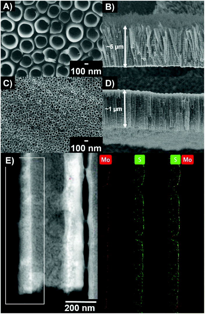 | ||
| Fig. 1 SEM images of the as-prepared TiO2 nanotube (TNT) layers: (A, C) top-view, and (B, D) cross-sectional view of 5 μm and 1 μm thick TNT layers. (E) STEM HAAD image and the corresponding STEM EDX elemental maps (obtained from the marked region) show the decoration of Mo and S species on the TNT wall and reveal a homogeneous MoS2 decoration along the TNT wall after 2 MoS2 ALD cycles. | ||
For the purpose of comparison, we used TNT layers with 3 different ALD MoS2 cycles: 1, 2 and 5. After the ALD of MoS2, it was possible to observe MoS2 ultrathin nanosheets on TNT layers only by TEM (not SEM), due to their extremely small dimensions. Fig. 1E shows a representative STEM HAAD image and the corresponding STEM EDX elemental maps of the chemical distribution of Mo and S elements on the fragment of a nanotube wall in the cross-sectional view after 2 MoS2 ALD cycles. This homogeneous decoration of TNT layers with MoS2 nanosheets was revealed over their entire volume. X-ray diffraction (XRD), micro-Raman spectroscopy (mRS) and X-ray photoelectron spectroscopy (XPS) were carried out to obtain additional information on the crystalline structure and composition (all in the ESI†). While XRD measurements could be carried out on TNT layers, mRS and XPS could be, due to the nature of these techniques and optimal signal-to-noise ratio, carried out only on planar Si wafers (ALD decorated in parallel with the TNT layers). The native SiO2 thin layer on the Si wafer was not removed before ALD decoration. From XRD patterns (Fig. S2†), only diffractions of TiO2 anatase and diffractions of Ti from the underlying Ti substrate were identified for blank TNT layers. In all MoS2 decorated TNT layers, additional diffraction of MoS2 at a 2θ of ∼14.3° is visible (26622-ICSD).45 This clearly shows the successful growth of crystalline MoS2 nanosheets during the ALD process. Nevertheless, several peaks are observed stemming from the nonstoichiometric MoXSY compositions. The presence of MoS2 is further confirmed by mRS (Fig. S3†). Signals at ∼384 cm−1 and ∼403 cm−1 which correspond to the E2g1 and A1g modes of MoS2, respectively, are observed (discussed in detail in the ESI†) when decorated by 5c MoS2.48 The obtained Raman spectra did not show any signal for 1c and 2c MoS2 due to the extremely small dimensions of the nanosheets. Only signals from the underlying substrate were observed. Nevertheless, the presence of MoS2 is confirmed by XPS for all ALD cycles (Fig. S4†). The high resolution spectra of Mo 3d show a doublet with the Mo 3d5/2 peak at 229.4 eV corresponding to the Mo4+ oxidation state and S 2p spectra show a doublet with the S 2p3/2 peak at 162.2 eV corresponding to the S2− oxidation state. The determined S/Mo ratios are 2.03, 2.13 and 2.31 for 1c, 2c and 5c MoS2, respectively. The doublet shape of Mo 3d is wider compared to that of pure MoS2.45 This is due to the presence of an additional Mo6+ oxidation state in the form of MoO3, which can have a two-fold origin. Either it is the result of a partial oxidation of Mo species following the ALD process or it stems from the reaction with the O species (in the TiO2 and SiO2) present on the interface between substrates and the decorated MoS2 nanosheets. Moreover, the decrease in O 1s peaks reflects the increasing amount of S–Mo–S stacks within nanosheets. The signal intensity follows the order 1 > 2 > 5 MoS2 ALD cycles (from the most intense to less intense).
The photoelectrochemical characteristics were recorded for blank and MoS2 decorated 5 μm thick TNT layers in the wavelength range from 310 nm to 800 nm, as shown in Fig. 2 and the ESI (Fig. S5†). The extension of the photocurrent responses into the visible spectral region relative to the blank TNT layers is observed for all TNT layers decorated with MoS2 nanosheets. Incident photon-to-electron conversion efficiency (IPCE, Fig. 2A) values were doubled for TNT layers with 1 and 2 MoS2 cycles, reaching ∼40%, in comparison with the blank TNT layer in the wavelength range of 350–370 nm. Due to the band gap of TiO2 of ∼3.2 eV there is no response in the VIS spectral region for blank TNT layers. In the wavelength range of 410–430 nm, the IPCE values reached ∼20% for TNT layers with 1 and 2 MoS2 cycles and about ∼10% for TNTs + 5c MoS2. This clearly shows a stronger ability of MoS2 decorated TNT layers to produce charge carriers and more separated e− compared to the blank layers. Also the annihilation of TiO2 surface states by MoS2 nanosheets might come into play, as shown previously.37 To examine the photoresponse of TNT layers over a range of wavelengths, the photocurrent transients were recorded at a fixed bias of +0.4 Vvs. Ag/AgCl with light on/off for 10 s period in the UV (Fig. 2B) and VIS spectral range (Fig. 2C). The MoS2 decorated TNT layers show a good photocurrent switching performance with a fast response time. The type-II heterojunction interface of the MoS2 (with a direct band gap)/TiO2 heterostructure and also the TiO2 surface state annihilation are responsible for such an enhancement.4,34,40 In contrast, an increased thickness of MoS2 nanosheets (i.e. theoretically 5 ALD cycles correspond to 5 S–Mo–S stacks with an indirect band gap) decreased the photoresponse in the UV spectral region compared to the blank layers. This is due to the low electron conductivity of MoS2 that limits the e− transfer.44,49 Moreover, with an increased number of ALD cycles, the increasing number of S–Mo–S stacks could significantly suppress the e− transfer in the direction perpendicular to the basal plane of the MoS2 nanosheets.49
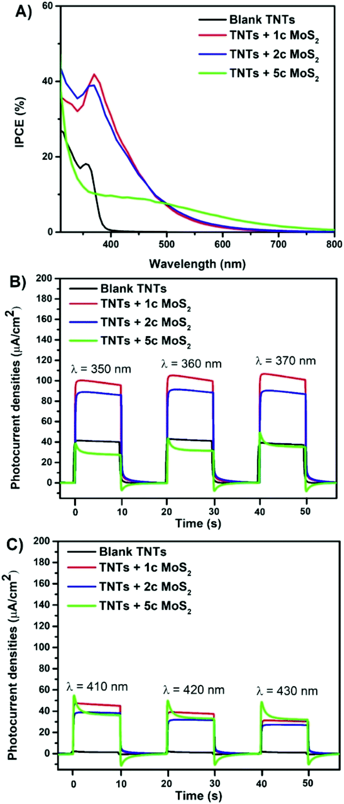 | ||
| Fig. 2 (A) Incident photon-to-electron conversion efficiency (IPCE) vs. wavelength. Photocurrent transients recorded at (B) 350 nm, 360 nm, and 370 nm, respectively, and (C) 410 nm, 420 nm, and 430 nm, respectively, for blank, and MoS2 decorated TNT layers. The “Xc” specifies the number of MoS2 ALD cycles. All data recorded in an aqueous 0.1 M Na2SO4 at 0.4 Vvs. Ag/AgCl. | ||
Fig. 3A and B show the photocatalytic performance (of the same TNT layers shown in Fig. 2) for the liquid phase photodegradation of methylene blue (MB) under UV and VIS irradiation, respectively. It follows a pseudo-first-order reaction.2 Thus, its kinetics can be expressed from the linear variation of ln![[thin space (1/6-em)]](https://www.rsc.org/images/entities/char_2009.gif) c/c0 as a function of time. The resulting kinetic rate constants are shown in Fig. 3.
c/c0 as a function of time. The resulting kinetic rate constants are shown in Fig. 3.
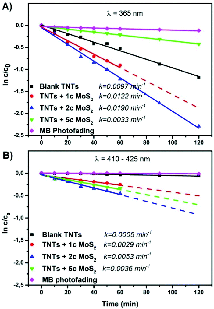 | ||
| Fig. 3 Liquid phase photocatalysis: degradation rates of methylene blue (MB) for blank and MoS2 decorated TNT layers and the resulting kinetic rate constants: (A) UV: λ = 365 nm and (B) VIS: λ = 410–425 nm. The “Xc” specifies the number of MoS2 ALD cycles. | ||
The results clearly show that the appropriate MoS2 decoration of TNT layers by 1 or 2 ALD cycles of MoS2 enhances the photocatalytic activity of TNT layers. TNT layers decorated with 5 ALD MoS2 cycles possess worse activities compared to the blank and to those with 1 or 2 cycles under UV irradiation (Fig. 3A). The band gap for this thickest MoS2 nanosheet decoration used in here is indirect,13,50 and it is mainly the excess of MoS2 on the available TiO2 surface that lowers the photocatalytic activity due to a shading effect.51,52 This means that MoS2 blocks the incident light absorption by TiO2 and reduces its photoexcitation capacity. Indeed, the higher density (and shading) of MoS2 nanosheets within TNT layers + 5c MoS2 compared to that in TNT layers + 2c MoS2 is clearly observed from STEM EDX (ESI, Fig. S6†). Fig. 3B shows the photodegradation of MB under VIS irradiation. Compared to the photodegradation in the UV spectral range, the photocatalytic activity of TNT layers + 5c MoS2 is enhanced and it is higher than that of TNT layers + 1c MoS2. Indeed, in the VIS spectral region, MoS2 is predominantly responsible for photodegradation due to its lower band gap compared to TiO2. Diffuse reflectance UV-VIS spectra and the corresponding Kubelka–Munk curves (ESI, Fig. S7†) were recorded to determine the optical band gap energy of blank and MoS2 decorated TNT layers. Values of ∼3.12 eV, ∼1.35 eV, and ∼1.19 eV for blank TNT layers, TNT layers + 1c MoS2, and TNT layers + 2c MoS2 were determined, respectively. The difference in the band gap energy can be described as follows. One ALD cycle results into one S–Mo–S stack. Therefore, with an increased number of ALD cycles, the number of S–Mo–S stacks also increases. As the band gap energy of MoS2 is strongly influenced by the number of S–Mo–S stacks, it will decrease with an increased number of these stacks. This suggests that the presence of MoS2 on the surface of TiO2 leads to the change in the electronic structure of TiO2. It is apparent that TNT layers decorated by 1 or 2 ALD cycles of MoS2 possess an increased incident light absorption. For the TNT layers + 5c MoS2, it was not possible to measure any reflectivity, due to extremely black colour of the samples. Furthermore, the photocatalytic activity strongly depends on the quantity of the exposed edge sites of MoS2.18 An increase in the MoS2 nanosheet thickness leads to smoothing its surface, thus decreasing the area of the exposed edge sites of MoS2.53 This is due to the non-ideal growth mode, which takes place, when layered materials such as MoS2, are synthesized by thermal ALD53 and also by the very nature of MoS2 formation. Indeed, the active edge sites of MoS2 and their formation were identified theoretically54 and experimentally55 for both crystalline56 and amorphous57 MoS2. These previous reports and results shown herein confirm that TNT layers + 2c MoS2 (theoretically 2 S–Mo–S stacks) rendered the best photocatalytic performance in the liquid phase under both UV and VIS light irradiation, due to a higher amount of exposed edge sites compared to TNT layers + 1c MoS2 and TNT layers + 5c MoS2.
Gas phase photodegradation in Fig. 4 shows kinetics and the total hexane-to-CO2 conversion achieved on the blank and MoS2 decorated TNT layers. The more detailed mechanism of hexane-to-CO2 conversion is described in the ESI.† The highest photocatalytic conversion of hexane was achieved for 1 and 2 MoS2 cycle decorated TNT layers with 34% and 21% conversion, removing the total of 5 μmol and 3 μmol of hexane which is ∼5 and ∼3 times higher compared to that of blank, respectively. The 5 MoS2 cycle decoration of TNT layers did not show any measurable photoactivity.
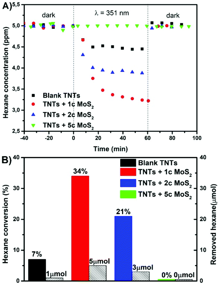 | ||
| Fig. 4 Gas phase photocatalysis: (A) changes in the hexane concentration in the reactor upon UV light irradiation, (B) conversion and removal of hexane for blank and MoS2 decorated TNT layers. The “Xc” specifies the number of MoS2 ALD cycles. | ||
By comparing Fig. 3 and 4, it is clear that the best photocatalytic activities in both the phases are obtained for different MoS2 cycles (2c for the liquid and 1c for the gas phase). The reasons for this are not understood yet and require further investigation. However, while the difference in the homogeneity of the ALD MoS2 nanosheets between the different nanotube layers used for the liquid and gas phase photocatalysis can be ruled out, the difference in the reactivity of the side edges of the MoS2 nanosheets produced by 1c and 2c ALD cycles towards hexane degradation and diffusional and MoS2 shading aspects of the different nanotube layers (with different morphological features) in general cannot be excluded.
Conclusions
In conclusion, the homogeneous decoration of TNT layers with MoS2 nanosheets using ALD was demonstrated in this work. The ALD MoS2 decorated TNT layers possess enhanced photocurrent densities with improved charge carrier transport and increased photocatalytic activities, in both phases (liquid and gas). The presented results clearly show how promising is the combination of 1D supports with 2D materials. These results may also pave the way for more sophisticated devices and applications of these nanomaterial classes in future.Conflicts of interest
There are no conflicts to declare.Acknowledgements
The authors acknowledge the financial support from the European Research Council (ERC no. 638857) and the Ministry of Education, Youth and Sports of the Czech Republic (projects LM2015082, LO1411, LQ1601 and LTACH17007).Notes and references
- J. M. Macak, M. Zlamal, J. Krysa and P. Schmuki, Small, 2007, 3, 300–304 CrossRef CAS PubMed.
- M. Zlamal, J. M. Macak, P. Schmuki and J. Krýsa, Electrochem. Commun., 2007, 9, 2822–2826 CrossRef CAS.
- I. Paramasivam, H. Jha, N. Liu and P. Schmuki, Small, 2012, 8, 3073–3103 CrossRef CAS PubMed.
- H. Sopha, M. Krbal, S. Ng, J. Prikryl, R. Zazpe, F. K. Yam and J. M. Macak, Appl. Mater. Today, 2017, 9, 104–110 CrossRef.
- D. Regonini, G. Chen, C. Leach and F. J. Clemens, Electrochim. Acta, 2016, 213, 31–36 CrossRef CAS.
- N. R. De Tacconi, C. R. Chenthamarakshan, G. Yogeeswaran, A. Watcharenwong, R. S. De Zoysa, N. A. Basit and K. Rajeshwar, J. Phys. Chem. C, 2006, 110, 25347–25355 CrossRef CAS PubMed.
- L. Tsui, T. Homma and G. Zangari, J. Phys. Chem. C, 2013, 117, 6979–6989 CrossRef CAS.
- J. M. Macák, H. Tsuchiya, A. Ghicov and P. Schmuki, Electrochem. Commun., 2005, 7, 1133–1137 CrossRef.
- K. Zhu, N. R. Neale, A. Alexander Miedaner and A. J. Frank, Nano Lett., 2007, 7, 69–74 CrossRef CAS PubMed.
- A. L. Linsebigler, G. Lu and J. T. Yates, Chem. Rev., 1995, 95, 735–758 CrossRef CAS.
- M. R. Hoffmann, S. T. Martin, W. Choi, D. W. Bahnemann and W. M. Keck, Chem. Rev., 1995, 95, 69–96 CrossRef CAS.
- K. Rajeshwar, J. Appl. Electrochem., 1995, 25, 1067–1082 CrossRef CAS.
- Z. Li, X. Meng and Z. Zhang, J. Photochem. Photobiol., C, 2018, 35, 39–55 CrossRef CAS.
- J. Theerthagiri, R. A. Senthil, B. Senthilkumar, A. Reddy Polu, J. Madhavan and M. Ashokkumar, J. Solid State Chem., 2017, 252, 43–71 CrossRef CAS.
- R. G. Dickinson and L. Pauling, J. Am. Chem. Soc., 1923, 45, 1466–1471 CrossRef CAS.
- X. Zhou, M. Licklederer and P. Schmuki, Electrochem. Commun., 2016, 73, 33–37 CrossRef CAS.
- D. Dumcenco, D. Ovchinnikov, K. Marinov, P. Lazi, M. Gibertini, N. Marzari, O. Lopez Sanchez, Y.-C. Kung, D. Krasnozhon, M.-W. Chen, S. Bertolazzi, P. Gillet, A. Fontcuberta Morral, A. Radenovic and A. Kis, ACS Nano, 2015, 9, 4611–4620 CrossRef CAS PubMed.
- Y.-J. Yuan, H.-W. Lu, Z.-T. Yu and Z.-G. Zou, ChemSusChem, 2015, 8, 4113–4127 CrossRef CAS PubMed.
- W. Zhou, Z. Yin, Y. Du, X. Huang, Z. Zeng, Z. Fan, H. Liu, J. Wang and H. Zhang, Small, 2013, 9, 140–147 CrossRef CAS PubMed.
- Z. Xiong, L. L. Zhang and X. S. Zhao, Chem. – Eur. J., 2011, 17, 2428–2434 CrossRef CAS PubMed.
- S.-M. Lam, J.-C. Sin, A. Z. Abdullah and A. R. Mohamed, J. Mol. Catal. A: Chem., 2013, 370, 123–131 CrossRef CAS.
- M. Sabarinathan, S. Harish, J. Archana, M. Navaneethan, H. Ikeda and Y. Hayakawa, RSC Adv., 2017, 7, 24754–24763 RSC.
- M. Mehta, A. P. Singh, S. Kumar, S. Krishnamurthy, B. Wickman and S. Basu, Vacuum, 2018, 155, 675–681 CrossRef CAS.
- W. Teng, Y. Wang, H. Huang, X. Li and Y. Tang, Appl. Surf. Sci., 2017, 425, 507–517 CrossRef CAS.
- M. Sun, Y. Wang, Y. Fang, S. Sun and Z. Yu, J. Alloys Compd., 2016, 684, 335–341 CrossRef CAS.
- Y. Yu, J. Wan, Z. Yang and Z. Hu, J. Colloid Interface Sci., 2017, 502, 100–111 CrossRef CAS PubMed.
- H. N. T. Phung, V. N. K. Tran, L. T. Nguyen, L. K. T. Phan, P. A. Duong and H. V. T. Le, J. Nanomater., 2017, 2017, 1–6 CrossRef.
- Y. Yu, S.-Y. Huang, Y. Li, S. N. Steinmann, W. Yang and L. Cao, Nano Lett., 2014, 14, 553–558 CrossRef CAS PubMed.
- D. Voiry, M. Salehi, R. Silva, T. Fujita, M. Chen, T. Asefa, V. B. Shenoy, G. Eda and M. Chhowalla, Nano Lett., 2013, 13, 6222–6227 CrossRef CAS PubMed.
- E. Parzinger, B. Miller, B. Blaschke, J. A. Garrido, J. W. Ager, A. Holleitner and U. Wurstbauer, ACS Nano, 2015, 9, 11302–11309 CrossRef CAS PubMed.
- C. Meng, Z. Liu, T. Zhang and J. Zhai, Green Chem., 2015, 17, 2764–2768 RSC.
- D. Wang, Y. Xu, F. Sun, Q. Zhang, P. Wang and X. Wang, Appl. Surf. Sci., 2016, 377, 221–227 CrossRef CAS.
- F. Dvorak, R. Zazpe, M. Krbal, H. Sopha, J. Prikryl, S. Ng, L. Hromadko, F. Bures and J. M. Macak, Appl. Mater. Today, 2019, 14, 1–20 CrossRef.
- M. Krbal, J. Prikryl, R. Zazpe, H. Sopha and J. M. Macak, Nanoscale, 2017, 9, 7755–7759 RSC.
- D. Voiry, M. Salehi, R. Silva, T. Fujita, M. Chen, T. Asefa, V. B. Shenoy, G. Eda and M. Chhowalla, Nano Lett., 2013, 13, 6222–6227 CrossRef CAS PubMed.
- Y.-J. Yuan, Z.-J. Ye, H.-W. Lu, B. Hu, Y.-H. Li, D.-Q. Chen, J.-S. Zhong, Z.-T. Yu and Z.-G. Zou, ACS Catal., 2016, 6, 532–541 CrossRef CAS.
- J. Liang, C. Wang, P. Zhao, Y. Wang, L. Ma, G. Zhu, Y. Hu, Z. Lu, Z. Xu, Y. Ma, T. Chen, Z. Tie, J. Liu and Z. Jin, ACS Appl. Mater. Interfaces, 2018, 10, 6084–6089 CrossRef CAS PubMed.
- C. Liu, L. Wang, Y. Tang, S. Luo, Y. Liu, S. Zhang, Y. Zeng and Y. Xu, Appl. Catal., B, 2015, 164, 1–9 CrossRef CAS.
- D. Wang, Y. Xu, F. Sun, Q. Zhang, P. Wang and X. Wang, Appl. Surf. Sci., 2016, 377, 221–227 CrossRef CAS.
- Y. Tian, Y. Song, M. Dou, J. Ji and F. Wang, Appl. Surf. Sci., 2018, 433, 197–205 CrossRef CAS.
- L. Yang, X. Zheng, M. Liu, S. Luo, Y. Luo and G. Li, J. Hazard. Mater., 2017, 329, 230–240 CrossRef CAS PubMed.
- L. Guo, Z. Yang, K. Marcus, Z. Li, B. Luo, L. Zhou, X. Wang, Y. Du and Y. Yang, Energy Environ. Sci., 2018, 11, 106–114 RSC.
- H. Feng, N. Tang, S. Zhang, B. Liu and Q. Cai, J. Colloid Interface Sci., 2017, 486, 58–66 CrossRef CAS PubMed.
- L. Zheng, S. Han, H. Liu, P. Yu and X. Fang, Small, 2016, 12, 1527–1536 CrossRef CAS PubMed.
- H. Sopha, A. Tesfaye, R. Zazpe, J. Michalicka, F. Dvorak, L. Hromadko, M. Krbal, J. Prikryl, T. Djenizian and J. M. Macak, FlatChem, 2019, 17, 100130 CrossRef.
- M. Motola, L. Satrapinskyy, T. Roch, J. Subrt, J. Kupcik, M. Klementova, M. Jakubickova, F. Peterka and G. Plesch, Catal. Today, 2017, 287, 59–64 CrossRef.
- H. Sopha, M. Baudys, M. Krbal, R. Zazpe, J. Prikryl, J. Krysa and J. M. Macak, Electrochem. Commun., 2018, 97, 91–95 CrossRef CAS.
- H. Li, Q. Zhang, C. C. R. Yap, B. K. Tay, T. H. T. Edwin, A. Olivier and D. Baillargeat, Adv. Funct. Mater., 2012, 22, 1385–1390 CrossRef CAS.
- L. Yang, C. Xie, J. Jin, R. Ali, C. Feng, P. Liu, B. Xiang, L. Yang, C. Xie, J. Jin, R. N. Ali, C. Feng, P. Liu and B. Xiang, Nanomaterials, 2018, 8, 463 CrossRef PubMed.
- A. Kuc, N. Zibouche and T. Heine, Phys. Rev. B: Condens. Matter Mater. Phys., 2011, 83, 245213 CrossRef.
- Y.-J. Yuan, Z.-J. Ye, H.-W. Lu, B. Hu, Y.-H. Li, D.-Q. Chen, J.-S. Zhong, Z.-T. Yu and Z.-G. Zou, ACS Catal., 2016, 6, 532–541 CrossRef CAS.
- D. B. Nimbalkar, H.-H. Lo, P. V. R. K. Ramacharyulu and S.-C. Ke, RSC Adv., 2016, 6, 31661–31667 RSC.
- T. A. Ho, C. Bae, S. Lee, M. Kim, J. M. Montero-Moreno, J. H. Park and H. Shin, Chem. Mater., 2017, 29, 7604–7614 CrossRef CAS.
- B. Hinnemann, P. G. Moses, J. Bonde, K. P. Jørgensen, J. H. Nielsen, S. Horch, A. I. Chorkendorff and J. K. Nørskov, J. Am. Chem. Soc., 2005, 127, 5308–5309 CrossRef CAS PubMed.
- T. F. Jaramillo, K. P. Jørgensen, J. Bonde, J. H. Nielsen, S. Horch and I. Chorkendorff, Science, 2007, 317, 100–102 CrossRef CAS.
- J. Bonde, P. G. Moses, T. F. Jaramillo, J. K. Nørskov and I. Chorkendorff, Faraday Discuss., 2009, 140, 219–231 RSC.
- C. G. Morales-Guio and X. Hu, Acc. Chem. Res., 2014, 47, 2671–2681 CrossRef CAS PubMed.
Footnote |
| † Electronic supplementary information (ESI) available: Experimental procedures, SEM and STEM HAAD characterization of the materials, photocurrents, Kubelka–Munk curves, XPS, XRD, micro-Raman and details of hexane photodegradation. See DOI: 10.1039/c9nr08753b |
| This journal is © The Royal Society of Chemistry 2019 |