
 Open Access Article
 This Open Access Article is licensed under a Creative Commons Attribution-Non Commercial 3.0 Unported Licence
Tailoring metal-dielectric nanocomposite materials with ultrashort laser pulses for dichroic color control†
N.
Sharma
a,
N.
Destouches
 *a,
C.
Florian
b,
R.
Serna
b and
J.
Siegel
*b
*a,
C.
Florian
b,
R.
Serna
b and
J.
Siegel
*b
aUniv Lyon, UJM-Saint-Etienne, CNRS, Institut d Optique Graduate School, Laboratoire Hubert Curien UMR 5516, F-42023 Saint-Etienne, France. E-mail: nathalie.destouches@univ-st-etienne.fr
bLaser Processing Group, Instituto de Optica, Consejo Superior de Investigaciones Científicas (IO-CSIC), Serrano 121, 28006 Madrid, Spain. E-mail: j.siegel@csic.es
First published on 1st October 2019
Abstract
Metal-dielectric nanocomposites are multiphase material systems containing nanostructures, whose size and arrangement determine the optical properties of the material, enabling the production of new materials with custom-designed response. In this paper, we exploit a femtosecond laser-based strategy to fabricate nanocomposites based on silver nanoparticles (Ag NPs) with tunable optical spectral response. We demonstrate how the spectral response, specifically color and dichroic response, is linked to Ag NPs growth and self-organization processes that are controlled locally by the choice of the laser irradiation parameters, such as scan speed and laser light polarization. When the scan speed increases, the Ag NPs are formed at larger depths below the film surface and give rise to the formation of embedded NPs gratings. As a result, the effective optical properties of the films are strongly modified enabling the display of a broad range of solid colors in the visible region. Furthermore, the choice of the laser light polarization allows to fabricate films either with iridescent or dichroic properties (linear polarization) or with non-diffractive and non-dichroic colors (circular polarization). Finally, the high spatial control over the transformed areas achieved with the laser processing, allows the building of hybrid nanostructures by means of interlacing structures with different optical responses. These results demonstrate the high potential of fs-laser technology to process Ag-based nanocomposites to fabricate coatings with a designed reflectivity, transmission, diffraction, as well as polarization anisotropy response. The Ag nanocomposites investigated in this work hold great promise for a broad range of applications especially for coloring, for enhanced visual effects, and for smart information encoding for security applications.
Introduction
Metal nanoparticles (NPs) are key players in modern strategies to fabricate nanocomposite materials with exceptional properties, not offered by nature. Interaction with light triggers collective oscillations of electrons at the NP surface, also known as localized surface plasmon resonance (LSPR), which determines the optical response of the system. The LSPR is related to the size, shape, separation and orientation of the NPs, along with the refractive index of the surrounding matrix. Although this dependence provides an opportunity for tailoring the spectral response of the system to match specific applications,1–3 the interrelation of all parameters complicates this problem enormously. Thus, most fabrication techniques fail to produce NPs with a high degree of symmetry, featuring broad distributions in size, shape, orientation, and consequently only weak SPRs.Another possibility for shaping the optical response of a material is by arranging NPs with moderate symmetry and size distribution into gratings or lattices with medium or long-range order. The optical response of such “superstructure” can be tuned conveniently by changing the grating or lattice period, which is simpler than tuning individual NP characteristics. Fabricating such structures with top-down approaches such as lithography, in which a pattern is imprinted by photons, electrons or ions, would be prohibitive in terms of time and cost. A superior methodology is to exploit self-organization processes, a bottom-up technique which is capable of arranging micro- and nanometer size objects to form extended periodic structures.4,5
One strategy to fabricate such NP structures is based on the use of nanostructured substrates in order to achieve controlled growth of regular arrays of silver nanoparticle chains6 or stripes.7 Another approach, not requiring the use of patterned substrates, is based on physical vapor deposition at glancing angle combined with subsequent laser treatment, leading to preferential melting and merging of certain NPs.8 Both techniques, are limited to obtain non-protected NP structures located at the substrate surface, which is troublesome in case of silver, which degrades through oxidation, accompanied by a corresponding change in its SPR.9
Although the above fabrication techniques can be complemented by an additional step of cover layer deposition to protect the NPs, single-step techniques would be desirable as they result in lower fabrication costs of devices. Such single-step nanostructure fabrication techniques can be grouped in two approaches: the first one is based on re-shaping and re-ordering, which exploits the high peak intensity of low repetition rate femtosecond (fs) laser pulses to change the NP shape and even re-arrange them, overcoming the large forces exerted by the dielectric matrix.10–12 The second approach relies on the use of porous dielectric titania films loaded with silver nanoparticles, in which nucleation, growth and self-organization can be triggered by irradiation with continuous wave (cw) laser light.13 Recently, the beneficial influence of thermal accumulation using femtosecond laser pulses was reported for such systems, enabling the growth of silver nanoparticle structures in mesoporous amorphous TiO2 films.14
In the present work, we demonstrate the vast potential of femtosecond laser pulses to create metal-dielectric nanocomposites with silver particle sizes, shapes and arrangement that can be controlled by suitably altering the scan speed of the laser beam. The different nanoparticle configurations lead to pronounced spectral changes that can be exploited both, in reflection and transmission to create a broad range of colours. Moreover, we also demonstrate how the choice of laser polarization allows us either to generate or to prevent polarization anisotropy in the spectral response of the samples. In addition, a fabrication strategy based on interlacing two different nanocomposite structures produced with two different scan speeds is used, yielding hybrid nanostructures. The broad spectral range covered by the different structures illustrates their potential for smart visual effects and other photonics-based applications.
Results and discussion
The material system is composed of a thin mesoporous film of amorphous TiO2 loaded with silver salt and small silver NPs (<3 nm) on glass substrate (see “Materials and methods”).13 The nanoparticles feature a weak absorption band in the blue/green spectral region corresponding to a LSPR, which is excited resonantly by a high repetition rate femtosecond laser at 515 nm wavelength. The laser is focused onto the film and scanned at a speed ‘v’ over the surface (see “Materials and methods”). This irradiation scheme triggers a number of complex processes, including LSPR excitation, hot electron generation, silver ion ejection and reduction, heating, Ostwald ripening, coalescence, and NP growth, accompanied by a crystallization and collapse of the mesoporous TiO2 matrix.14 The structures formed were characterized with scanning electron microscopy (SEM), atomic force microscopy (AFM) and high angle annular dark field scanning transmission electron microscopy (HAADF-STEM), the spectral responses with a spectrophotometer, while the phase transition of the matrix was monitored using Raman spectroscopy (see “Materials and methods”).Nanocomposite morphologies and topographies: influence of the scanning speed
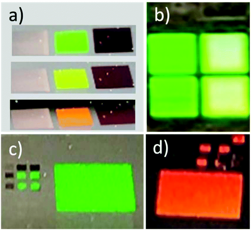
The laser parameters of this study were chosen to investigate the formation of the nanocomposite structures as a function of scan speed, ranging from 1 mm s−1 to 200 mm s−1 at a constant laser peak fluence (F = 47 mJ cm−2). Each structure was laser-written with a 2 μm spacing between scan lines and covered an area of 9 mm2. The homogeneity of the structures achievable with the fabrication method can be best appreciated by optical inspection of the colour change for speeds ranging from 1 to 170 mm s−1. Above 170 mm s−1, the colour starts fading. Fig. 1 shows images of different laser written areas recorded with a smartphone camera, illustrating smart visual effects of the dichroic colours produced using a change of the scan speed. The difference in colour between reflection and transmission illustrates the complex spectral response, which will be discussed later.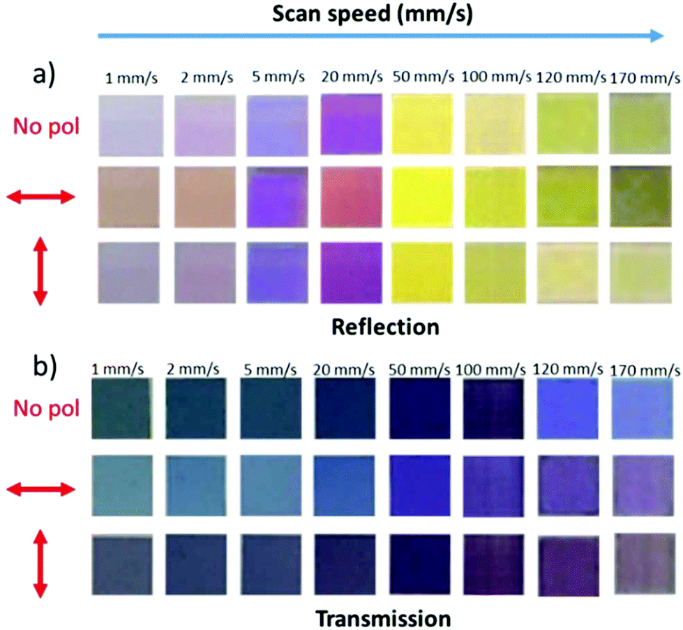 | ||
| Fig. 1 Colour changes induced by the formation of nanostructures. Illustration of the colour changes induced by scanning high repetition rate femtosecond laser pulses over the sample surface at different speeds and constant peak fluence. Each square is imprinted over an area of 9 mm2. Illumination was provided by a white light source for unpolarized (No pol) and horizontally/vertically polarized light (denoted by double sided arrows) and the image was recorded with a smartphone camera (a) in reflection and (b) in transmission. | ||
The different nanostructures responsible for these optical responses were investigated using SEM and AFM. Fig. 2 shows the respective SEM and AFM images of four different nanocomposite structures obtained at speeds of 1, 20, 100 and 170 mm s−1. In all cases, the thermal effects resulting from the high repetition rate of the laser (500 kHz) induce the growth of Ag NPs, which can be observed by SEM in the range of 10 nm–80 nm. While differences in NP size between the four structures can be appreciated (see ESI†), the most striking difference is the change in the NP arrangement, caused by different self-organization processes. At a high speed of v = 170 mm s−1 (Fig. 2(d)), a surface grating is formed with an amplitude of 50 nm and a period of Λ170 mm s−1 = 498 ± 20 nm. The NPs mainly grow on the top surface and their top view shape is either spherical or elongated but with no particular orientation. A decrease in the scan speed to v = 100 mm s−1 (Fig. 2(c)) leads to a surface grating whose amplitude and period are smaller, at 40 nm and 474 ± 20 nm respectively, and in which NPs start getting buried. This structure is similar to one of the structures reported in our former work14 obtained at this speed and belongs to the class of laser-induced periodic surface structures (LIPSS).15–21
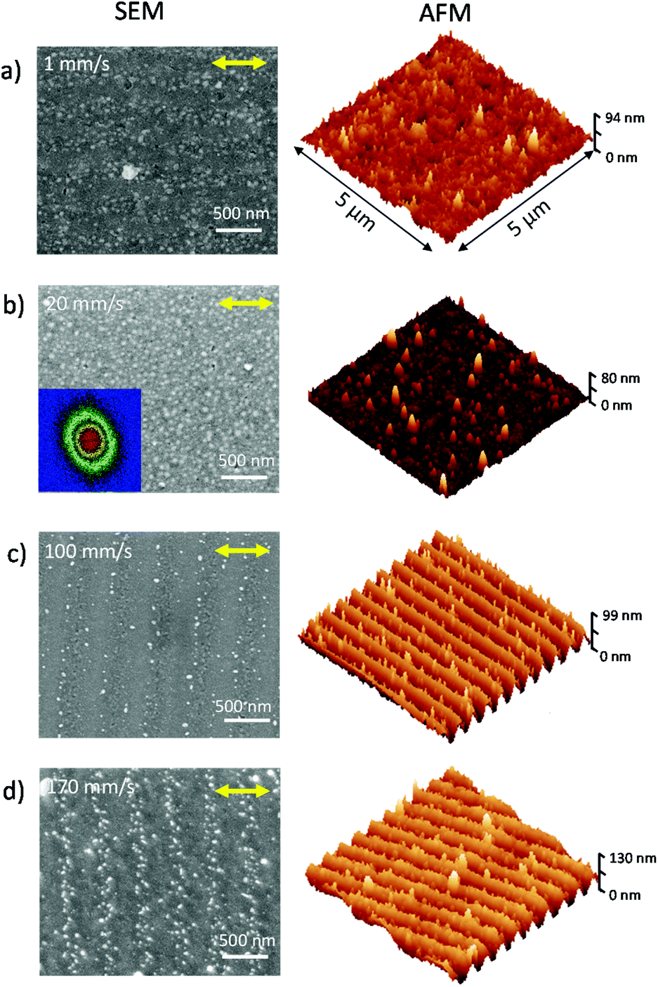 | ||
| Fig. 2 Surface morphology and topography. Illustration of the evolution of the nanocomposite structure with the scan speed, characterized by their respective SEM and AFM images for (a) 1 mm s−1 (b) 20 mm s−1 (c) 100 mm s−1 and (d) 170 mm s−1 scan speeds. The embedded grating (EG) for speed v = 1 mm s−1 is formed parallel to the laser polarization (depicted by double side yellow arrows), whereas the surface grating (SG) at v = 100 mm s−1 and 170 mm s−1 is oriented perpendicular to the laser polarization. The inset in (b) shows a fast Fourier transform (FFT) of the corresponding SEM image. | ||
LIPSS can be formed when a material is exposed to multiple short or ultrashort laser pulses at energies above the modification threshold.15,22–24 The underlying mechanism of this self-organization process is attributed to the interference of the incident laser light with a surface wave, which leads to a periodic intensity modulation that is imprinted into the material.25 While the nature of the surface wave (surface plasmon polariton propagation or light scattering) is still under debate, the omnipresence of LIPSS is astonishing, appearing in metals,26–28 semiconductors,21,29–31 and dielectrics.19,32–37 LIPSS can feature different sizes, shapes and orientations that are determined by a complex interplay of laser irradiation and material parameters. The most common type of LIPSS are so called “ripples” or low spatial frequency LIPSS oriented perpendicular to the laser polarization, to which the ones observed in the present manuscript belong.
When decreasing the speed to v = 20 mm s−1 (Fig. 2(b)), the NPs distribute randomly beneath the TiO2 surface with a high density and slightly larger size from 20 nm, growing up to 80 nm in size (Fig. S3†). The inset in Fig. 2(b) shows a fast Fourier transform (FFT) of the SEM image, illustrating a slight anisotropy related to the laser polarization. The shape of the FFT pattern might indicate a NP shape slightly elongated along the laser polarization. An influence of the laser polarization on the shape of silver nanoparticles was reported previously in different systems and resulted from a series of processes, which were well described by Stalmashonak et al.,38 following the excitation of hot electrons through plasmonic absorption, metallic NPs ionize after releasing electrons in the surrounding matrix mainly along the laser polarization, where the field enhancement is higher. The ionization is followed by an isotropic Ag+ ion ejection. The latter can reduce on the nanoparticles again, along the axis where electrons are concentrated, leading to NPs that tend to elongate along the laser polarization.11,12,39 Further, at the lowest scan speed of v = 1 mm s−1 (Fig. 2(a)), the NPs self-arrange into horizontal stripes, parallel to the laser polarization, with a period Λ1 mm s−1 = 344 ± 20 nm. This NP structure is embedded inside the titania matrix, which can be seen by the low contrast of the white embedded Ag NPs compared to the random single NPs that can be seen at the sample surface. The fact, that the NP grating is embedded can also be appreciated by the AFM map displayed in Fig. 2(a), featuring no visible periodic surface structure. This structure is similar to one of the structures reported in our former work obtained at 10 mm s−1,14 but shows no residual periodic surface modulation perpendicular to the grating. It is worth emphasizing that this grating structure is fundamentally different from the surface grating observed at v = 100 mm s−1 and 170 mm s−1, since it is aligned parallel to the laser polarization, rather than perpendicular and is embedded inside the film with a significantly smaller period.
The results shown in Fig. 2 clearly demonstrate the existence of two different grating types, along with the transition from one type to the other. For simplicity, the two types are referred as, embedded grating ‘EG’ (formed at low speed) and, surface grating ‘SG’ (formed at high speed). The underlying reason, why a change of the scan speed leads to this strong change in the nanostructure, is related to the different pulse number per spot diameter incident on a given area (see “Materials and methods”). Depending on the pulse number, and so on the amount of deposited energy, the relative weight of the numerous laser-induced processes is changed, leading to the different kinds of nanostructures. A description of the mechanisms involved in the formation of these different types of nanostructures that explains the transition between the different regimes with the scan speed (deposited energy) is proposed below.
As shown in our previous works,40 the initial sample contains a high density of small NPs mainly located in the top part of the mesoporous TiO2 film. Under low power fs laser excitation at 515 nm, single photon absorption occurs in the nanocomposite film through the localized surface plasmon resonance (LSPR) of Ag NPs, and leads to the generation of hot electrons on NPs. Charge transfers from the excited NPs to the TiO2, which are known to occur during each fs laser pulse,41 are likely to transiently turn the top part of the film into a metal-like film and allow excitation of a surface plasmon polariton (SPP).42 The interference of this SPP with the incident wave modulates the energy deposition with a period that depends on the laser wavelength as described further. The amplitude of the SPP is initially small due to the randomness of the silver NPs and heterogeneities that initially excite it. However, such a perturbation can be enhanced by a positive feedback when the grating starts forming, provided that the laser polarization appears as transverse magnetic (TM) for the grating, i.e. as perpendicular to the grating lines, since SPPs are only excited in such a configuration. When forming such a surface grating, Ag NPs mainly grow on the top surface (Fig. 2d) when the pulse number per spot diameter is low (low thermal accumulation) and mainly grow embedded in the film, when the number of accumulated pulses increases (Fig. 2c). Further, as shown in the film cross-section in Fig. 5, the very smooth surface grating that forms in such conditions mainly results from a local densification of the mesoporous film rather than matter ablation.
When increasing the pulse number per spot diameter, thermal accumulation becomes higher and NPs grow more, leading to less charge transfers from the NP surface to the surrounding matrix (decrease of the surface/volume ratio), to more optical scattering in the film (larger size), and to an increased absorption by the LSPR (stronger heating). The reduced number of hot electrons transferred to the titania matrix is expected to affect the metal-like behaviour and the excitation of the surface mode. At the same time, the increased heating in the film tends to crystallize the titania matrix and collapse the film mesostructure independently of the surface grating, thus leading to flattening of the surface profile. All of this leads to the second kind of nanostructure (Fig. 2b), at speeds between 5 and 70 mm s−1, with larger embedded NPs uniformly distributed with a poor residual surface grating that tends to disappear for an increased number of pulses (lower speeds). Moreover, NPs slightly elongate along the laser polarization direction according to the mechanisms described above.
Finally, when the pulse number per spot diameter is increased further, the light scattering of grown embedded NPs favours the excitation of guided modes, which for the surface grating is enhanced by the embedded grating formation. However, the condition for triggering a positive feedback now differs from what was expected when exciting a surface plasmon polariton. Here, the guided mode excitation is enhanced only if the grating orientation is parallel to the incident polarization (only the transverse electric (TE) polarization allows efficient diffraction into a guided mode). This condition therefore creates a positive feedback, leading to the generation of an embedded NP grating parallel to the laser polarization. This is what is observed experimentally at the low speed of v = 1 mm s−1 (Fig. 2a).
For both, the guided and surface modes, the grating period is calculated as 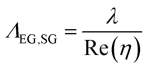 , where λ is the laser wavelength (515 nm) and Re(η) is the real part of the complex effective index experienced by the propagating mode.42,43 For the guided mode, Re(η) = ngm, which corresponds to the effective refractive index of the guided mode when the embedded grating starts forming. The grating period values of the different structures (determined from SEM images) are plotted as a function of the scan speed in Fig. 3. For v = 5 mm s−1, where embedded nanogratings (EG) are formed with parallel orientation to the laser polarization, the grating period was measured as Λ5 mm s−1 = 329 ± 20 nm. The period increases slightly towards lower speeds, yielding a maximum value of Λ1 mm s−1 = 344 ± 20 nm. Both values are consistent with the mechanism of embedded grating formation via a guided mode with ngm ranging between 1.50 and 1.57. The latter should be larger than the refractive index of the glass substrate, 1.46, and lower than the refractive index of the mesoporous titania film loaded with silver nanoparticles. Interestingly, the measured periods are also consistent with the one obtained for embedded nanogratings obtained using continuous-wave (cw) laser on the same nanocomposites in previous works (Λcw-laser = 318 nm, with λ = 530 nm and v = 0.6 mm s−1).13 The similarity of the structures formed upon ultrashort or cw laser irradiation, in particular the very similar scan speed values used, suggests that the underlying mechanisms are comparable. This hypothesis is supported by the fact that the ultrashort laser pulses are delivered with a very high repetition rate (f = 500 kHz), which leads to a strong heat accumulation effect and therefore generating similar thermal conditions as for cw laser irradiation when accumulating a large pulse number per spot diameter.
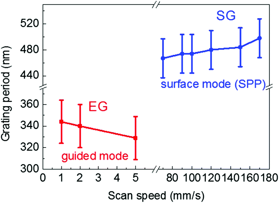 | ||
| Fig. 3 Speed dependence of the grating period. Evolution of the period of the nanostructures that feature gratings with the scan speed. For speeds in the range v = 1–5 mm s−1, an embedded grating (EG) is formed inside the film and its orientation is parallel to the laser polarization. For the range v = 70–170 mm s−1, a surface grating (SG) is formed, whose orientation is perpendicular to the laser polarization. In between the two regimes, no grating is formed in the film, but Ag NPs with a slightly elongated shape are observed. | ||
For surface mode excitation, the physics is different. Due to the high initial density of small silver NPs in the TiO2 film, combined with the large peak intensity of the femtosecond laser that leads to an increase of the free electron density in the TiO2, the material develops a metal-like state and plasmonic behaviour. This allows coupling of the laser light into a surface plasmon polariton (SPP), which propagates along the direction of the electric field vector. In this case, the relevant effective refractive index for the grating period can be obtained from 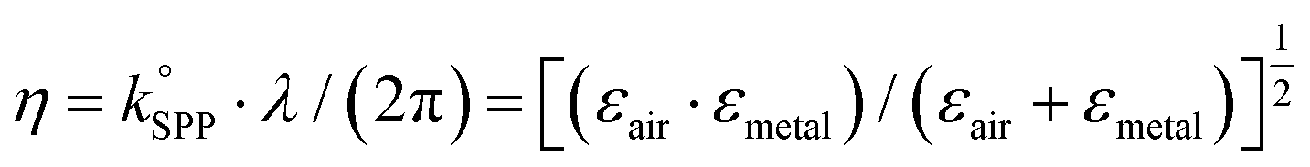 , with
  being the SPP wavevector on a planar air–metal interface with εair and εmetal being the dielectric functions of air and metal. Typically, for metals Re(η) ≈ 1, which yields a grating period that is close to the laser wavelength used, ΛSG ≈ 515 nm.44
At the lowest speed within this range, surface ripples with a period of Λ70 mm s−1 = 467 ± 30 nm are formed. The period gradually increases with speed up to Λ170 mm s−1 = 498 ± 30 nm. As discussed above, the grating is formed by interference of SPPs with the incident pulse, and the period is thus expected to depend on the effective dielectric constant of the film surface. Using the above relation, values in the range of 1.0 < Re(η) < 1.1 are obtained. The implication of η being a function of the scan speed is actually reasonable, since the effective pulse number per spot diameter is expected to change the size and density of the NPs as well as the TiO2 density, and therefore affects the effective dielectric constant. Furthermore, it can be mentioned that for speeds between 200 mm s−1 and 1000 mm s−1, randomly distributed NPs were formed at the surface (not shown). One of the conclusions that can be drawn from Fig. 3 is that a change in the scan speed, and thus the effective number of pulses, leads to a temperature change inside the nanocomposite, thus altering the final nanostructure. In order to study the maximum temperature increase experienced by the film during laser processing, the fabricated nanostructures were examined with a low power Raman spectrometer (see “Materials and methods”), in order to detect the possible formation of the crystalline phase in the TiO2 matrix with a change in the scan speed. Usually, the presence of the anatase phase can be identified in the Raman spectra by its characteristic Eg bands at 144 and 633 cm−1 and B1g and A1g bands at 409 and 515 cm−1, respectively. Moreover, this allows an approximate estimation of the experienced temperature increase, since the formation of the anatase phase in our TiO2 films is known to occur progressively when increasing the temperature from 100 °C to 900 °C.45
Fig. 4 shows a series of Raman spectra recorded in areas fabricated at different scan speeds. Three bands were detected in the study, with an increasing amplitude for a decreasing scan speed. The small peak amplitude observed at higher speeds is characteristic of a low density of nanocrystals in the amorphous titania matrix. At the lowest scan speed of v = 1 mm s−1, the Raman spectrum has the highest amplitude of the anatase phase peaks, revealing the presence of a higher density of the crystalline phase, which is however only partial if compared with one of our previous work.45 In comparison, crystallization is nearly inexistent at the highest speed (200 mm s−1) where no grating formation occurs. This leads to the conclusion that only partial crystallization of the matrix is achieved with femtosecond pulse irradiation and only at low scan speed. As different phases have different dielectric functions, the partial crystallization and densification of the film (collapse of pores) may be a reason for the observed change in grating period as a function of scan speed, in both speed regimes.
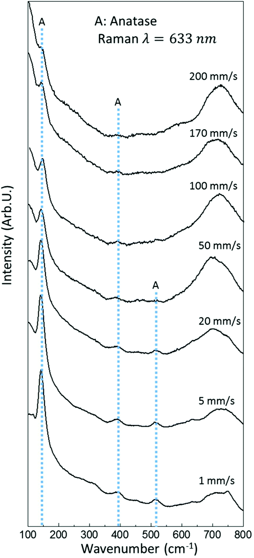 | ||
| Fig. 4 Influence of the scan speed on the phase of the TiO2 matrix. Raman spectra for the different nanostructures obtained using different scan speeds, as indicated. ‘A’ denotes different bands corresponding to the crystalline anatase phase of titania, namely the Eg band at 144 cm−1 and the B1g and A1g bands at 409 and 515 cm−1. | ||
For surface grating structures, the partially crystallized matrix regions are actually mainly located in the grating grooves. This can be observed in Fig. 5 for a structure written at 100 mm s−1, displaying a HAADF-STEM image of a SG cross section, accompanied by their respective diffraction patterns. The latter feature diffraction spots in the valleys, corresponding to both anatase TiO2 and fcc Ag nanocrystals (Fig. 5b) and broad rings on the hills, corresponding to the amorphous phase of TiO2, respectively.
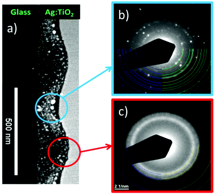 | ||
| Fig. 5 Locally dependent nanoparticle growth and matrix crystallization in SG structures: (a) HAADF-STEM image of film cross-section cut perpendicular to LIPSS for a structure written at 100 mm s−1. (b–c) Diffraction patterns of the blue and red encircled zones in the HAADF-STEM image. | ||
Optical response of the nanocomposites
In order to assess their optical response, the nanostructures were characterized using a spectrophotometer. For each structure, spectra for both light polarizations were recorded, parallel (∥) and perpendicular (⊥) to the laser polarization, in order to investigate the possible presence of anisotropic optical responses. Fig. 6 shows the measured transmission (T) spectra of the four different nanostructures shown in Fig. 2. The corresponding reflectance (R) and absorption (1-R-T) spectra are shown in the ESI† but not included here in order to better appreciate the spectral trends. As a reference for the reader, the corresponding spectra of an infiltrated nanocomposite film before laser exposure are shown in Fig. 6(a), which shows a very high transmission, and thus weak absorption, throughout the visible range and no dichroism.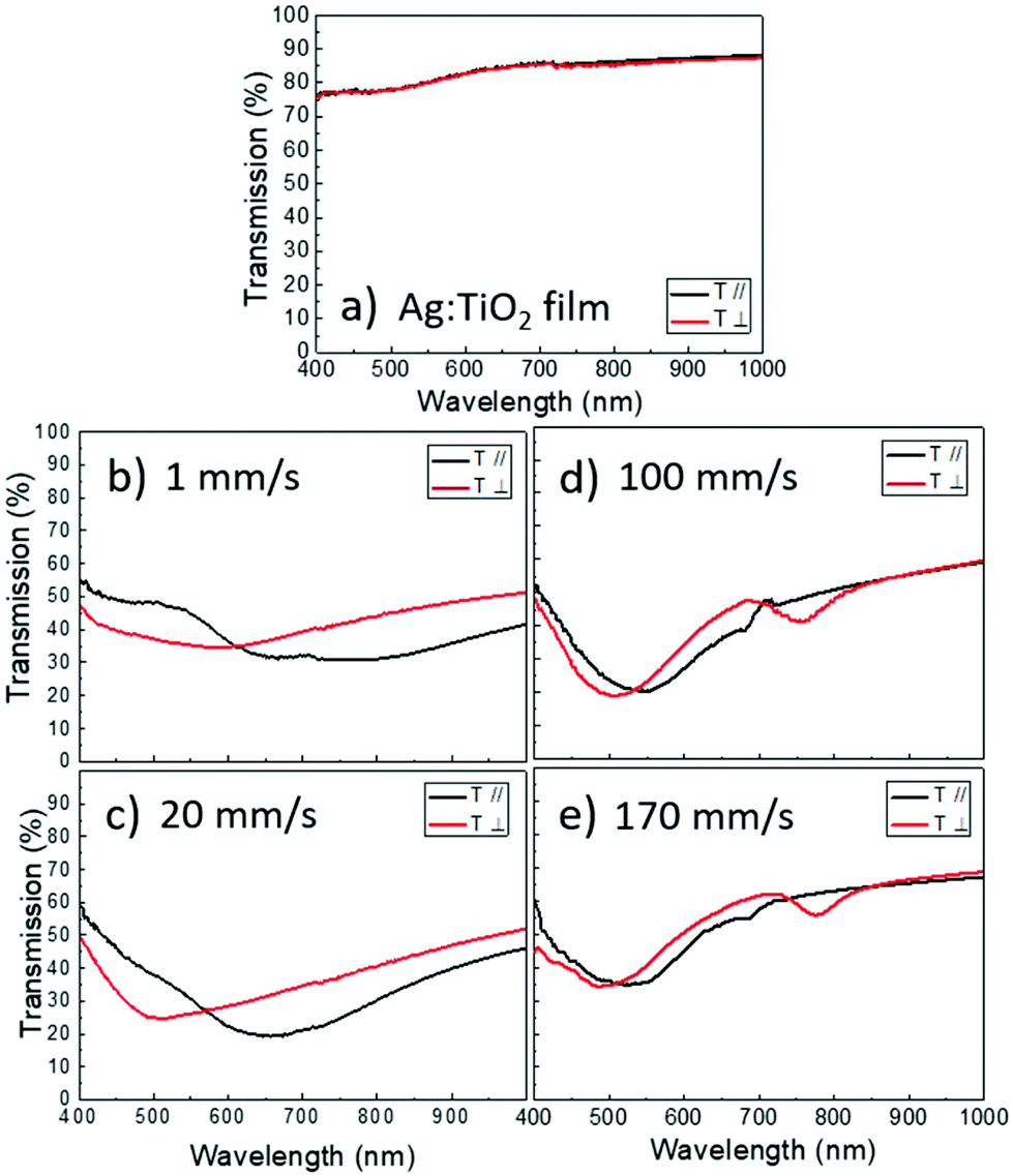 | ||
Fig. 6 Spectral response of the nanostructures. Transmission (T) spectra taken at 6° incidence angle for (a) the initial Ag![[thin space (1/6-em)]](https://www.rsc.org/images/entities/char_2009.gif) :TiO2 nanocomposite films before laser irradiation and different scan speeds of (b) 1 mm s−1, (c) 20 mm s−1, (d) 100 mm s−1, and (e) 170 mm s−1. ⊥ and ∥ refers to the probe polarization, respective to the laser polarization. Reflectance (R) and loss spectra (including absorption and scattering) are shown in the ESI.† :TiO2 nanocomposite films before laser irradiation and different scan speeds of (b) 1 mm s−1, (c) 20 mm s−1, (d) 100 mm s−1, and (e) 170 mm s−1. ⊥ and ∥ refers to the probe polarization, respective to the laser polarization. Reflectance (R) and loss spectra (including absorption and scattering) are shown in the ESI.† | ||
At the lowest speed (v = 1 mm s−1), the features of both spectra are broad and little pronounced, with a minimum transmission of about 30%. The most striking observation is the existence of a polarization anisotropy reflected in the spectral shift of about 200 nm between the two minima. As the scan speed is increased, the spectral features become more pronounced, while the anisotropy is reduced. At v = 20 mm s−1, well-defined minima are observed in the visible spectral region, reaching values down to 20%. In this case, the presence of strong polarization anisotropy is most likely caused by the shape anisotropy of the silver nanoparticles (see FFT inset in Fig. 2(b)), since there is no evidence of a NP grating. Such a strong dichroism due to a NP shape anisotropy with preferential orientation was also reported in other works on femtosecond laser irradiation of silver nanoparticles embedded in different dielectric matrices.11,12,46,47 In the work of Stalmashonak et al., the initial shape of the spherical silver NPs were altered using low repetition rate (1 kHz) fs laser irradiation to lengthen or shorten the NPs along the laser polarization direction (depending on the irradiation conditions), yielding optical dichroism in the material.38 Similarly, Baraldi et al. showed polarization anisotropy of a near-coalescence single layer of silver NPs using fs laser irradiation, altering the shape, alignment and organization of the NPs.12
At v = 100 mm s−1 and 170 mm s−1, the transmission minima are further sharpened and the polarisation anisotropy is reduced. Moreover, additional spectral bands appear in the infrared region near 800 nm. These bands correspond to the probe light that is coupled into the film acting as a waveguide, leading to a lower transmission and reflection and to a higher absorption. Coupling is mediated by the surface grating. The fact that no such band is observed at 1 mm s−1, although the structure also features a grating, suggests that the coupling efficiency of a surface grating is higher than that of an embedded grating. This additional band can be conveniently used to estimate the effective refractive index of the nanostructured film using the equation: 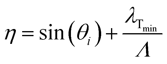 , where θi is the incidence angle and λTmin, the wavelength at which transmission shows a minimum which is close to the resonance wavelength, even though not exactly the same. For v = 100 mm s−1 the grating structure has a period of 474 nm, and from the spectrum we obtain λTmin = 760 nm, for θi = 6°. The calculation yields η = 1.71, which is an approximation of the effective index value for the guided mode in the nanostructured film. At 760 nm wavelength, the 474 nm period grating does not diffract light in free space, since
 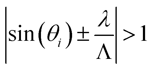 for incidence angles smaller than −37°, depicting that the decreased transmission is mainly due to absorption. The dichroism observed in all structures is directly related to the laser polarization, either by determining a preferential direction of surface or guided mode coupling or by lengthening the nanoparticles along a certain direction. This strong dichroism observed in the processed samples (Fig. 1 and 6) can be exploited in a variety of applications for example for encoding and counterfeiting materials, as well as for smart decorative purposes.
The diffraction properties of the two different grating types are illustrated in Fig. 7. White light diffraction20 at three different observation angles is caused by the embedded grating (EG) formed at 1 mm s−1, shown in Fig. 7(a). Further, strong diffraction for a single angle by four different surface gratings (SG) formed at different speeds (90 mm s−1–150 mm s−1) is shown in Fig. 7(b).
 | ||
| Fig. 7 Photographs of nanostructured samples, showing diffraction of white light of (a) an embedded grating (central square written at 1 mm s−1) observed at 3 different angles; (b) four surface gratings (written at 90, 100, 120, 150 mm s−1). Frames (c) and (d) show the same hybrid grating (large square, see also Fig. 9), observed from two different directions, rotated by 90°. | ||
As shown in Fig. 1, illumination of the different structures with non-polarized white light produces different colours in reflection and transmission, compared to illumination with linearly polarized light. Similar colors can be produced by using circular polarized laser light for the fabrication of structures. The obtained structures feature colors that are non-dichroic and non-diffractive. Fig. 8 displays the T spectra of two representative nanocomposite films that were irradiated with a circular polarized laser, using scan speeds of 1 and 100 mm s−1.
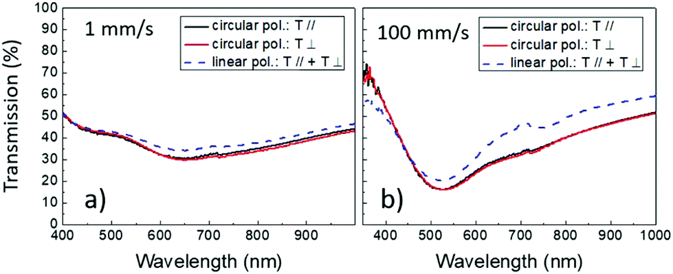 | ||
| Fig. 8 Elimination of spectral anisotropy by structuring with circular polarized laser light. Transmission (T) spectra for nanostructures fabricated with circular polarized laser light for two different scan speeds. (a) 1 mm s−1 and (b) 100 mm s−1. For comparison, curves are included for structures fabricated with linear polarized laser light, obtained by calculating the average value of the experimental ⊥ and ∥ curves from Fig. 6(b) and (d). ⊥ and ∥ refers to the probe beam polarization, respective to the laser polarization and their orientations are maintained for irradiation with circular polarized light. The corresponding reflectance (R) and loss spectra (1-R-T) are shown in the ESI.† | ||
It can be seen immediately that any signs of anisotropy disappear when using circular polarized light. Moreover, the obtained spectra are very similar to the average spectrum of the structures written with linear polarized light measured with parallel and perpendicular polarizations (Fig. 6(b) and (d)). Although for v = 100 mm s−1 the resulting average curves are similar, they show a significant deviation in the infrared region due to the existence of grating coupling and mode propagation for the structures fabricated with linear polarized laser light, and the absence of this behaviour for circular laser light. The general similarity of the spectral response for both laser polarizations underlines its importance for applications and the usefulness of this approach, which allows to fabricate nanostructures with a similar spectral response and optional dichroism.
Hybrid nanostructures
While the above results exploit a change of the scan speed to achieve spectral tuning of the laser-fabricated samples, a complementary strategy is applied to combine different nanostructures placed close together. New spectra can be synthesized in this way via linear combination of the spectra of the two individual nanostructures. The idea is implemented by means of interlacing nanostructures of two different types, each produced within single scan lines with an approximate width of about 23 μm. The particular hybrid nanostructure shown in Fig. 9 was fabricated by first writing a large array with a line spacing of 46 μm at a laser scan speed of 100 mm s−1 and subsequently writing a second array at 1 mm s−1, which was laterally displaced by 23 μm in order to fill the gaps of the first array.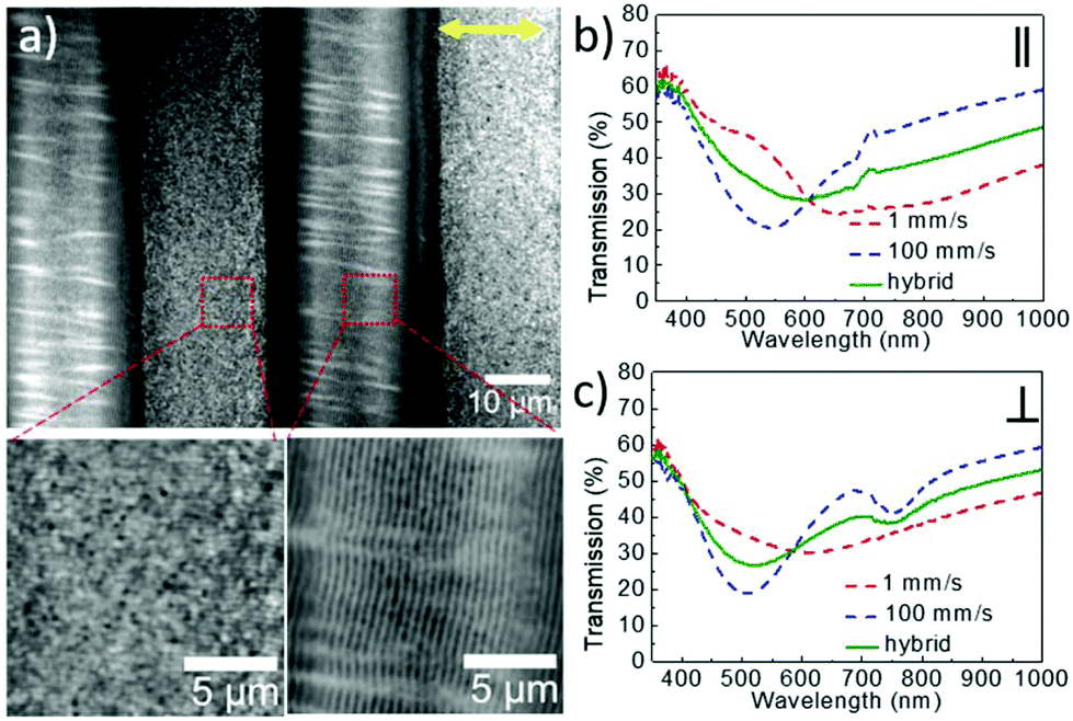 | ||
| Fig. 9 Hybrid nanostructure. (a) Optical micrographs of a hybrid nanostructure composed of adjacent vertical scan lines, each containing a different type of nanograting. Magnified regions are shown below, the left corresponding to the EG (barely visible horizontal grating lines) and the SG (vertical grating lines). (b) and (c) Measured transmission spectra of the hybrid nanostructure for both light polarizations (∥ and ⊥), compared to the corresponding spectra of areas written at single speeds, 1 and 100 mm s−1. | ||
This led to the formation of interlaced lines, as shown in Fig. 9(a), each with a different grating period (ΛEG = 330 nm and ΛSG = 480 nm) and orthogonal orientations. The linear laser polarization was kept the same in both cases, aligned along the scan direction, as shown in the optical micrographs (Fig. 9(a)). The fact, that the used line spacing was more than 20 times larger than for the homogeneous structures using a line separation of 2 μm, led to a strong decrease of the effective pulse number per spot diameter within a line. Thus, it was necessary to compensate for this effect by rescanning each line 20 times in order to accumulate an equivalent pulse number as for the homogenous areas. This method enabled the formation of adjacent embedded gratings (EG) and surface gratings (SG).
Fig. 9(b) and (c) show the transmission spectra of the hybrid structure to light polarized perpendicular and parallel to the laser polarization direction, respectively. Since the adjacent gratings are narrow-spaced, the perceived transmission spectra of the hybrid structure are essentially the sum of the individual spectra of the two gratings obtained at 1 and 100 mm s−1. The simultaneous presence of two orthogonal gratings is illustrated in Fig. 7(c and d), showing light diffraction for a hybrid structure in two different incidence/observation planes, rotated by 90°.
This strategy of interlacing different nanostructures enables the predictive design of new spectra based on the knowledge of the spectra of the two participating individual structures. This approach can be sophisticated by changing the relative weight of an individual structure through a deviation from a 1:1 interlacing ratio, towards 2:1 or 3:1. Likewise, more than two different nanostructures can participate in the design of a new spectrum. Such parametric study opens ways for the fabrication of customized hybrid structures for a range of different applications.
Conclusions
This work demonstrates the fabrication of Ag-based nanocomposite structures using a fs laser scanning technique, to trigger the controlled growth and self-organization of Ag NPs. By adjusting the scan speed, the NPs are selectively formed either at the surface or embedded inside the film and can self-organize according to different optical mechanisms. At low laser scan speeds, NP organization is governed by the excitation of a guided mode inside the film and large Ag NPs are grown, enabled by the occurrence of a high temperature rise. Raman spectroscopy reveals a partial crystallization of the titania matrix in its anatase phase and demonstrates an increase in the nanocrystal content for the lower scan speeds. At high laser scan speeds, the ultrashort laser pulses induce transient excitation of surface modes in form of surface plasmon polaritons due to the high density of small NPs in the initial film. As a result, laser-induced periodic surface structures are created, giving rise to the formation of silver NPs ordered along the grating lines.The induced Ag NP growth and self-organization processes lead to a marked color change of the nanostructured composite thin film, which can be controlled by the scan speed. Furthermore, in this work we also demonstrate two methods to prepare either dichroic color or diffractive films by a proper selection of the laser light polarization and scan speed. First, by using linear polarized laser pulses a strong dichroism in reflection and transmission is generated. Dichroism is found to be caused by the presence of the different grating structures formed in the films for high and low scan speeds, as well as by the shape anisotropy of the NPs induced at moderate scan speeds. The films with dichroism show iridescent properties that can be useful for encoding information in counterfeiting applications. Second, by using circularly polarized laser light for processing, films with non-dichroic and non-diffractive color perception have been prepared. In this case, the produced nanostructures do not show neither a preferential shape nor orientation. Finally, the flexibility of this laser-based marking technology also allows the fabrication of complex hybrid nanostructures composed of different adjacent nanostructure types, interlaced to cover large areas. Such generation, design and combination of multiple nanostructures on micrometer-sized areas with ultrashort pulsed lasers offer further control over the optical response of the Ag nanocomposite systems. This methodology opens the route for improved laser marking technology to achieve enhanced visual effects, and for smart information encoding for security applications.
Materials and methods
Mesoporous titania films
The substrates used were microscopic glass slides of 1 mm thickness from Thermo Scientific with SiO2, Na2O, CaO and MgO as the major components. The refractive index of the glass is 1.5171 and density 2.479. The films were elaborated on these substrates by sol–gel process consisting of titanium tetraisopropoxide (TTIP, Aldrich; 97%), acetylacetone (AcAc, Aldrich; 99%), hydrochloric acid (HCl, Roth; 37%), ethanol (EtOH, Carlo Erba; absolute), Pluronic P123 ((PEO)20(PPO)70(PEO)20 (Aldrich; MW: 5000), and ultrapure water (H2O) with specific molar ratios at: TTIP:P123:EtOH:HCl:H2O:AcAc::1:0.025:28.5:0.015:29.97:0.5, as published previously in our articles.48 The films were annealed at 340 °C, to obtain mesoporous amorphous titania thin films with a thickness of 200 ± 30 nm.
Nanocomposite films
The titania pores are then filled with silver ionic solution, by soaking the films in 1.5 M silver ionic solution. The ions are further converted to smaller atoms and nanoparticles by UV irradiation (254 nm, 6 mW cm−2, 10 min), thanks to the photocatalytic activity of titania with initial size of silver NPs being 1–3 nm.49Laser processing
The laser system used was a fiber-amplified femtosecond laser system with a pulse duration of 340 fs and a fundamental wavelength of 1030 nm, working at a repetition rate frep = 500 kHz. In order to excite the LSPR of the silver NPs, the fundamental wavelength was frequency doubled to 515 nm, using a BBO crystal. This assures the non-absorption of this wavelength by the titania matrix or the glass substrate, the laser peak fluence being low enough not to allow two-photon absorption by the latter.50 The incident pulse peak fluence (F = 2E/πω02, where E is the pulse energy and ω0 is the laser beam waist) was adjusted using a half-wave plate combined with a thin film polarizer, which was followed by another half-wave plate or quarter-wave plate for controlling the laser polarization. The beam is delivered by a galvanometric scanning system combined with an F-theta lens of focal length 10 cm, focusing the laser beam on the sample surface with a beam diameter d = 2ω0 = 33 μm (1/e2 intensity). The explored scan speed range was v = 1–200 mm s−1, and the line separation used was in all cases Δ = 2 μm, except for the hybrid structures written, where Δ = 46 μm was used. The corresponding effective pulse number per spot diameter in each case can be calculated for overlapping scan lines as Neff,2D = (π·(d/2)2·frep)/(v·Δ), and for single scan lines as Neff,1D = d·frep/v.Characterizations
A FEI Nova nanoSEM 200, scanning electron microscopy (SEM), was used in low vacuum mode with a helix detector to measure the surface morphology. This allows to measure the morphology of the sample under vacuum without any conductive coating. FIB thin lamellae were made using a focused ion beam/scanning electron microscope (FIB/SEM) FEI Helios 600i. The film was protected by carbon layers of increasing density deposited by evaporation, electron beam, and ion beam to prevent charging effect and ion damage of the film. FIB/SEM process was chosen to extract a lamella from the exact middle of a laser scanned line. Rough milling, U cut, transfer of the lamellae on a transmission electron microscopy (TEM) half grid, thinning was carried out. Particular attention was paid to the cleaning of the lamellae at several decreasing ion beam voltages, down to 1 kV. High angle annular dark field scanning transmission electron microscopy (HAADF-STEM) micrographs were measured with a Jeol 2010F TEM operated at 200 kV.The period of the gratings and the error was calculated using ImageJ software while calculating the period over two different magnified SEM images. A Cary 5000 spectrophotometer (Agilent) was used to measure the transmission and the reflectance of the irradiated nanostructures under a 6° incidence angle. To study the topography of the nanostructures, an Agilent 5500 AFM was used in taping mode. Lastly, the Raman measurements were carried out using a LabRAM ARAMIS-Horiba Raman confocal spectrometer with an excitation wavelength of 633 nm, where the titania and the substrate were transparent.
Conflicts of interest
There are no conflicts to declare.Acknowledgements
The authors are grateful to Zeming Liu and Yaya Lefkir from Hubert Curien Laboratory for their contribution to the TEM characterizations. Measurements were done at CLYM, Lyon. The authors are also grateful to Francis Vocanson and Stéphanie Reynaud from the Laboratory Hubert Curien for elaborating the TiO2 films and preparing the FIB lamellae, respectively.This work was partially supported by the joint project SAMUL (2018FR0026) within the PICS programme between the CSIC and the CNRS. We acknowledge support of the publication fee by the CSIC Open Access Publication Support Initiative through its Unit of Information Resources for Research (URICI). JSi, RS and CF acknowledge the Spanish Ministry of Science, Innovation and Universities for financial support through research grants UDiSON (TEC2017-82464-R) and SENSIL (RTI2018-096498-B-I00) (MCIU/AEI/FEDER, UE), as well as the CSIC for the intramurales project 201850E057. ND and NS acknowledge the Region Auvergne Rhone-Alpes, ANR project MIXUP (ANR-18-CE39-0010) and LABEX MANUTECH-SISE (ANR-10-LABX-0075) of Université de Lyon, within the program Investissements d'Avenir (ANR-11-IDEX-0007).
References
- B. Palpant, Non-Linear Optical Properties of Matter, Springer Netherlands, 2006, p. 461 Search PubMed.
- M. Rycenga, C. M. Cobley, J. Zeng, W. Li, C. H. Moran, Q. Zhang, D. Qin and Y. Xia, Chem. Rev., 2011, 111, 3669 CrossRef CAS PubMed.
- M. J. Beliatis, S. J. Henley and S. R. P. Silva, Opt. Lett., 2011, 36, 1362 CrossRef CAS PubMed.
- C. Park, J. Yoon and E. L. Thomas, Polymer, 2003, 44, 6725 CrossRef CAS.
- S. Hyde, Z. Blum, T. Landh, S. Lidin, B. W. Ninham, S. Andersson and K. Larsson, The Language of Shape: The Role of Curvature in Condensed Matter: Physics, Chemistry, and Biology, Elsevier Science, 1996 Search PubMed.
- E. Fort, C. Ricolleau and J. Sau-Pueyo, Nano Lett., 2003, 3, 65 CrossRef CAS.
- J. R. Sanchez-Valencia, J. Toudert, A. Borras, A. Barranco, R. Lahoz, G. F. de la Fuente, F. Frutos and A. R. Gonzalez-Elipe, Adv. Mater., 2011, 23, 848 CrossRef CAS PubMed.
- A. Nicolas Filippin, A. Borras, V. J. Rico, F. Frutos and A. R. González-Elipe, Nanotechnology, 2013, 24, 045301 CrossRef CAS PubMed.
- J. L. Elechiguerra, L. Larios-Lopez, C. Liu, D. Garcia-Gutierrez, A. Camacho-Bragado and M. Jose Yacaman, Chem. Mater., 2005, 17, 6042 CrossRef CAS.
- M. Kaempfe, T. Rainer, K. Berg, G. Seifert and H. Graener, Appl. Phys. Lett., 1999, 74, 1200 CrossRef CAS.
- A. Stalmashonak, C. Matyssek, O. Kiriyenko, W. Hergert, H. Graener and G. Seifert, Opt. Lett., 2010, 35, 1671 CrossRef CAS PubMed.
- G. Baraldi, J. Gonzalo, J. Solis and J. Siegel, Nanotechnology, 2013, 24, 255301 CrossRef CAS PubMed.
- N. Destouches, N. Crespo-monteiro, G. Vitrant, Y. Lefkir, S. Reynaud, T. Epicier, Y. Liu, F. Vocanson and F. Pigeon, J. Mater. Chem. C, 2014, 2, 6256 RSC.
- Z. Liu, J. Siegel, M. Garcia-Lechuga, T. Epicier, Y. Lefkir, S. Reynaud, M. Bugnet, F. Vocanson, J. Solis, G. Vitrant and N. Destouches, ACS Nano, 2017, 11, 5031 CrossRef CAS PubMed.
- J. F. Young, J. S. Preston, H. M. Van Driel and J. E. Sipe, Phys. Rev. B: Condens. Matter Mater. Phys., 1983, 27, 1155 CrossRef CAS.
- J. Bonse, J. Krüger, S. Höhm and A. Rosenfeld, J. Laser Appl., 2012, 24, 042006 CrossRef.
- Y. Fuentes-Edfuf, M. Garcia-Lechuga, D. Puerto, C. Florian, A. Garcia-Leis, S. Sanchez-Cortes, J. Solis and J. Siegel, Sci. Rep., 2017, 7, 4594 CrossRef PubMed.
- I. Gnilitskyi, T. J.-Y. Derrien, Y. Levy, N. M. Bulgakova, T. Mocek and L. Orazi, Sci. Rep., 2017, 7, 8485 CrossRef PubMed.
- A. Rudenko, J.-P. Colombier, S. Höhm, A. Rosenfeld, J. Krüger, J. Bonse and T. E. Itina, Sci. Rep., 2017, 7, 12306 CrossRef PubMed.
- N. Sharma, M. Vangheluwe, F. Vocanson, A. Cazier, M. Bugnet, S. Reynaud, A. Vermeulin and N. Destouches, Mater. Horiz., 2019, 6, 978 RSC.
- F. Gesuele, J. J. J. Nivas, R. Fittipaldi, C. Altucci, R. Bruzzese, P. Maddalena and S. Amoruso, Sci. Rep., 2018, 8, 12498 CrossRef PubMed.
- M. Birnbaum, J. Appl. Phys., 1965, 36, 3688–3689 CrossRef CAS.
- J. Bonse, S. Höhm, S. V. Kirner, A. Rosenfeld and J. Krüger, IEEE J. Sel. Top. Quantum Electron., 2017, 23, 9000615 Search PubMed.
- A. Ruiz de la Cruz, R. Lahoz, J. Siegel, G. F. de la Fuente and J. Solis, Opt. Lett., 2014, 39, 2491 CrossRef CAS PubMed.
- J. E. Sipe, J. F. Young, J. S. Preston and H. M. van Driel, Phys. Rev. B: Condens. Matter Mater. Phys., 1983, 27, 1141–1154 CrossRef CAS.
- J. P. Colombier, F. Garrelie, N. Faure, S. Reynaud, M. Bounhalli, E. Audouard, R. Stoian and F. Pigeon, J. Appl. Phys., 2012, 111, 024902 CrossRef.
- C. Florian, A. Mimidis, D. Puerto, E. Skoulas, E. Stratakis, J. Solis and J. Siegel, Beilstein J. Nanotechnol., 2018, 9, 2802–2812 CrossRef PubMed.
- B. Öktem, I. Pavlov, S. Ilday, H. Kalaycıoğlu, A. Rybak, S. Yavaş, M. Erdoğan and F. Ö. Ilday, Nat. Photonics, 2013, 7, 897–901 CrossRef.
- G. D. Tsibidis, C. Fotakis and E. Stratakis, Phys. Rev. B: Condens. Matter Mater. Phys., 2015, 92, 041405 CrossRef.
- M. Garcia-Lechuga, D. Puerto, Y. Fuentes-Edfuf, J. Solis and J. Siegel, ACS Photonics, 2016, 3, 1961–1967 CrossRef CAS.
- T. J. Y. Derrien, R. Koter, J. Krüger, S. Höhm, A. Rosenfeld and J. Bonse, J. Appl. Phys., 2014, 116, 074902 CrossRef.
- R. Wagner, J. Gottmann, A. Horn and E. Kreutz, Appl. Surf. Sci., 2006, 252, 8576–8579 CrossRef CAS.
- E. Rebollar, J. R. Vázquez de Aldana, I. Martín-Fabiani, M. Hernández, D. R. Rueda, T. A. Ezquerra, C. Domingo, P. Moreno and M. Castillejo, Phys. Chem. Chem. Phys., 2013, 15, 11287 RSC.
- J. Cui, A. Rodríguez-Rodríguez, M. Hernández, M. C. García-Gutiérrez, A. Nogales, M. Castillejo, D. Moseguí González, P. Müller-Buschbaum, T. A. Ezquerra and E. Rebollar, ACS Appl. Mater. Interfaces, 2016, 8, 31894–31901 CrossRef CAS PubMed.
- A. F. Sartori, S. Orlando, A. Bellucci, D. M. Trucchi, S. Abrahami, T. Boehme, T. Hantschel, W. Vandervorst and J. G. Buijnsters, ACS Appl. Mater. Interfaces, 2018, 10, 43236–43251 CrossRef CAS PubMed.
- A. Abdelmalek, B. Sotillo, Z. Bedrane, V. Bharadwaj, S. Pietralunga, R. Ramponi, E. H. Amara and S. M. Eaton, AIP Adv., 2017, 7, 105105 CrossRef.
- A. Y. Vorobyev and C. Guo, Laser Photonics Rev., 2013, 7, 385–407 CrossRef CAS.
- A. Stalmashonak, G. Seifert and H. Graener, Opt. Lett., 2007, 32, 3215 CrossRef CAS PubMed.
- A. Stalmashonak, A. Podlipensky, G. Seifert and H. Graener, Appl. Phys. B, 2009, 94, 459–465 CrossRef CAS.
- Z. Liu, G. Vitrant, Y. Lefkir, S. Bakthi and N. Destouches, Phys. Chem. Chem. Phys., 2016, 18, 24600–24609 RSC.
- A. Furube, L. Du, K. Hara, R. Katoh and M. Tachiya, J. Am. Chem. Soc., 2007, 129, 14852–14853 CrossRef CAS PubMed.
- F. Garrelie, J.-P. Colombier, F. Pigeon, S. Tonchev, N. Faure, M. Bounhalli, S. Reynaud and O. Parriaux, Opt. Express, 2011, 19, 9035 CrossRef CAS PubMed.
- A. E. Siegman and P. M. Fauchet, IEEE J. Quantum Electron., 1986, 22, 1384 CrossRef.
- A. Y. Vorobyev and C. Guo, J. Appl. Phys., 2008, 104, 063523 CrossRef.
- N. Sharma, H. Ma, T. Bottein, M. Bugnet, F. Vocanson, D. Grosso, T. Itina, Y. Ouerdane and N. Destouches, J. Phys. Chem. C, 2019, 123, 6070–6079 CrossRef CAS.
- J. Doster, G. Baraldi, J. Gonzalo, J. Solis, J. Hernandez-Rueda and J. Siegel, Appl. Phys. Lett., 2014, 104, 153106 CrossRef.
- A. Stalmashonak, A. Akin Unal, G. Seifert and H. Graener, in SPIE, 2008, pp. 70331Z–703318 Search PubMed.
- Z. Liu, T. Epicier, Y. Lefkir, G. Vitrant and N. Destouches, J. Microsc., 2017, 266, 60–68 CrossRef CAS PubMed.
- F. Tricot, F. Vocanson, D. Chaussy, D. Beneventi, S. Reynaud, Y. Lefkir and N. Destouches, RSC Adv., 2014, 4, 61305 RSC.
- B. Chimier, O. Utéza, N. Sanner, M. Sentis, T. Itina, P. Lassonde, F. Légaré, F. Vidal and J. C. Kieffer, Phys. Rev. B: Condens. Matter Mater. Phys., 2011, 84, 094104 CrossRef.
Footnote |
| † Electronic supplementary information (ESI) available: Reflectance, transmission and loss spectra of the initial and nanostructured films, particle size distributions. See DOI: 10.1039/c9nr06763a |
| This journal is © The Royal Society of Chemistry 2019 |