
 Open Access Article
 This Open Access Article is licensed under a
 Creative Commons Attribution 3.0 Unported Licence
Embedding epitaxial (blue) phosphorene in between device-compatible functional layers†
Carlo
Grazianetti
 *a,
Gabriele
Faraone
ab,
Christian
Martella
a,
Emiliano
Bonera
b and
Alessandro
Molle
*a
*a,
Gabriele
Faraone
ab,
Christian
Martella
a,
Emiliano
Bonera
b and
Alessandro
Molle
*a
aCNR-IMM Unit of Agrate Brianza, via C. Olivetti 2, Agrate Brianza, I-20864, Italy. E-mail: carlo.grazianetti@cnr.it; alessandro.molle@cnr.it
bDipartimento di Scienza dei Materiali, Università di Milano-Bicocca, via Cozzi 55, Milano, I-20125, Italy
First published on 27th September 2019
Abstract
The newly predicted allotropic phase of phosphorus termed blue phosphorus has been recently synthesized in its two-dimensional (2D) single layer fashion via epitaxial growth on a Au(111) substrate. The large scale epitaxy and the semiconductive character with a reported bandgap of ∼1.1 eV suggest that epitaxial phosphorene might be a suitable candidate to overcome the lack of a sizeable bandgap in semimetal X-enes. In close similarity to other X-enes, like silicene, the epitaxial phosphorene shows technological issues towards possible integration into devices, such as the metallic supporting template at the bottom and oxidation under ambient conditions on the top interface of its 2D lattice. Here, we report on a detailed structural and chemical analysis of epitaxial phosphorene and a newly developed methodology to allow for easy transfer of the chemically protected epitaxial phosphorene in between amorphous Al2O3 and thin Au(111) films grown on mica. The large scale epitaxy achieved on a portable Au(111)/mica template and the low reactivity with molecular oxygen of phosphorene pave the way for easy encapsulation of epitaxial phosphorene fostering its exploitability in devices through a versatile transfer methodology, as in the case of epitaxial silicene.
Introduction
The booming interest in the synthesis of artificial two-dimensional (2D) monoelemental lattices, so-termed X-enes, is mainly driven by the high expectations that these materials will accomplish great outcomes in the nanotechnology framework.1–5 Besides the fascinating challenge of synthesizing artificial 2D crystals not existing in nature, nowadays X-enes offer a great opportunity to tackle the technological challenges facing many fields, e.g. nanoelectronics or optoelectronics. The idea is to collect the largest portfolio of X-enes possible to satisfy the different requests of nanotechnology technological nodes. In this framework, mainly for periodic table kinship with graphene, silicene was synthesized first.6,7 Moreover, the recent integration of mono- and multi-layer silicene into field effect transistors (FETs) paved the way to exploit the X-enes beyond graphene for applications in nanotechnology.8,9 The proposed methodology enabling silicene integration has a general behaviour thus being potentially versatile to X-enes other than silicene. Such a process, initially termed Silicene Encapsulated Delaminated on Native Electrodes (SEDNE)8 is here extended to the concept of Universal X-ene Encapsulation, Decoupling and Operation (UXEDO) as a key-enabling methodology for device integration flow to the general class of X-enes.6 Here, we report on two key aspects of the UXEDO process by discussing the portability and stability of epitaxial phosphorene grown on Au/mica substrates and encapsulated with a protective capping layer.Results and discussion
The stable allotropes of elemental phosphorus are typically associated with colour names, i.e. white, red, violet, and black, based on the definition of the fundamental bandgaps.10–15 Among them, the most stable is black phosphorus, which recently successfully retraced the graphene's path being exfoliated down to a single layer, termed phosphorene.16 Although FETs and other devices based on exfoliated black phosphorus have been successfully fabricated,16–20 such a samples production method poses severe scalability issues towards a reliable integration of phosphorene into devices. In particular, the small flakes obtained by the exfoliation method do not look viable to be used in phosphorene-based nanotechnology.Zhu et al. noted that the armchair ridges in the side view of the black phosphorus can be converted into a new structure with zigzag puckering (Fig. 1a).21 Using ab initio calculations this postulated structural phase, called blue phosphorus, can be demonstrated to be as stable as black phosphorus, but most importantly is predicted to exhibit a wide fundamental gap in excess of 2 eV, hence the blue name. The optimized puckered honeycomb structure of single layer blue phosphorus has atoms covalently bonded at an equilibrium distance of 2.27 Å, with the hexagonal unit cell showing lattice vectors a1 and a2, with a modulus of 3.33 Å (Fig. 1a). Similarly to silicene,22 the first experimental evidence of blue phosphorus showed up as a reconstruction of the freestanding lattice. Zhang et al. reported on the monolayer blue phosphorus synthesis via molecular beam epitaxy (MBE) onto a Au(111) single crystal.23 Conversely, opposed to silicene, the phosphorene layer on Au(111) strikingly appears as a 2D semiconductor with an energy band-gap of ∼1.1 eV.23–26 By combining experimental and theoretical investigations, there is a consensus that the single layer blue phosphorus 4 × 4-reconstructed lattice matches the 5 × 5 Au(111) cell through a ∼9% tensile strain.24,25 This phase shows a characteristic flower-like morphology that looks more similar to the silicene 3 × 3 freestanding reconstruction, when grown on 4 × 4 Ag(111),7 than single layer black phosphorus, that is in turn characterized by a marked lattice anisotropy.
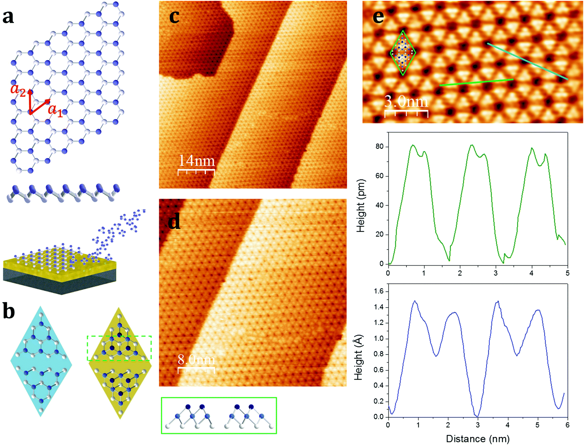 | ||
| Fig. 1 Top and side views of the freestanding lattice of blue phosphorene and the schematic representation of the growth through P4 molecules directed onto the Au(111) surface where they dissociate forming epitaxial phosphorene (a). Schematic models of the unit cell of the epitaxial phosphorene without (left) and with (right) the additional six phosphorus atoms per unit cell, as depicted in the green box showing the side view of the unit cell (b). STM images of the epitaxial phosphorene on Au(111) of 70 × 70 (c), 40 × 40 (d), and 8 × 15 (e) nm2 and the STM profiles along the green and blue lines. The green rhombus shows the unit cell as reported in the right panel of (b), i.e. the adatom-rich model, overlapped to the high-resolution STM topography. | ||
Hereafter, we refer to the 4 × 4-reconstructed single layer blue phosphorus on the 5 × 5 Au(111) as epitaxial phosphorene in order to avoid either cumbersome notation or misunderstanding with phosphorene derived from exfoliated black phosphorus. The first step towards the possible integration of epitaxial phosphorene relies on the use of Au(111) thin (300 nm) film on mica substrates (see the Experimental section) instead of expensive and hard-to-process Au(111) single crystals. Fig. 1c and d report on the scanning tunneling microscopy (STM) investigation of epitaxial phosphorene on Au(111)/mica templates. STM imaging shows large scale growth of a phosphorene film covering uniformly the substrate. In the substrate temperature range 240–270 °C, the growth process is self-limited and the key role is played by the catalytic activity of the gold substrate implicating the dissociative chemisorption of the incoming P4 molecules and hence the rearrangement of the adsorbed phosphorus atoms in a stable phosphorene layer (Fig. 1a).27 The overall quality of the epitaxial growth turns out to be improved by annealing the as-grown sample at the same growth temperature for 20 min. Limited to our survey and our phosphorus deposition method (see the Experimental section), we rule out the possibility to grow layers beyond the first one due to the self-limited growth mechanism, as evidenced by the constant P 2p/Au 4f core level ratio when increasing the deposition time as well as the STM topography showing the formation of phosphorus clusters (see Table S1 and Fig. S1 in the ESI†). Nonetheless, an accurate assessment of the single layer structure of phosphorene will be discussed below. Notably, at variance with silicene, so far just a single superstructure of epitaxial phosphorene has been reported and a single crystalline orientation is disclosed throughout our STM survey. If confirmed, in addition to the predicted high-electron mobility due to large strain (>104 cm2 V−1 s−1),25 this is a remarkable aspect because the grain boundaries are suspected to plague the carrier mobility in a similar material like silicene when operated as a transistor channel.8 The large scale STM topographies shown in Fig. 1c and d (see also Fig. S2 in the ESI†) are in good agreement with those reported, i.e. the overall morphology is dominated by the characteristic flower-like pattern.23–26 According to our statistics, we prove epitaxial phosphorene grows uniformly throughout the whole sample size thus providing compelling directions for a wafer scale production of epitaxial phosphorene. However, in the high-resolution images (Fig. 1e), we notice that the observed morphology does not match exactly with the proposed model reported in ref. 23–25 and recently questioned in ref. 26. Indeed, half the rhombus unit cell illustrated in Fig. 1b shows six atoms on the top layer (cyan, left panel) but the STM images conversely suggest that there are more likely three atoms (blue, right panel). Indeed, the blue STM line profile as shown in Fig. 1e indicates that there are two different heights, when crossing consecutive dark holes, thus suggesting the presence of a second layer on top of the modelled structure, as evidenced by the green box depicted in Fig. 1b showing a cross-sectional view of the unit cell. Indeed, the blue STM profile taken on the top layer shows that the additional three phosphorus atoms are placed at a distance of 0.5 Å on the top. Moreover, the green STM profile illustrated in Fig. 1e also shows that the lateral distance of the on-top phosphorus atoms on average is about 0.34 nm and they form a nearly regular triangular lattice. Therefore, according to ref. 26 we propose a model where the epitaxial phosphorene is decorated by three additional on-top phosphorus atoms placed in the hollow spots of the underlying hexagonal rings (see Fig. 1b), thus being an adatom-rich structure in between the mono- and bi-layer. This structure was confirmed by density functional theory calculations.26 Additional experiments are highly demanded to validate the theoretical model. The semiconductive behaviour of this adatom-rich structure is also confirmed by I(V) measurements performed through STM with a bandgap of ∼1 eV (see Fig. S3 in the ESI†). We cannot rule out that other reported structures can be obtained by finely tuning the growth parameters, but limited to our survey, the morphology is always consistent with that of the adatom-rich structure, that clearly spotlights a new type of vertically buckled honeycomb lattice differing from previously stated X-enes.1
The chemical bonding of epitaxial phosphorene has been scrutinized via X-ray photoelectron spectroscopy (XPS) by monitoring the core levels at each process step (see the Experimental section). The XPS spectra of Au 4f core levels before and after phosphorene growth show a negligible shift (<0.1 eV) indicative of the absence of alloying between gold and phosphorus (Fig. S4 in the ESI†). Fig. 2a reports on the P 2p core level that can be fitted by two components placed at 128.95 (P 2p3/2) and 129.81 (P 2p1/2) eV by taking into account the 0.86 eV spin-split. We observe that the P 2p core level is shifted to a lower binding energy than those of black (∼130 eV) and red (∼132 eV) phosphorus.28,29 Therefore the binding energy of the P 2p core level can be assumed to be a reliable marker for the identification of epitaxial phosphorene on gold. One critical aspect of X-enes is that their limited environmental stability out of the ultra-high vacuum (UHV) environment hampers any practical use. This is also the case for epitaxial phosphorene as it undergoes oxidation when exposed to air (after a few hours as depicted in Fig. 2b). Nonetheless, such an oxidation process takes place only partially, with a residual component of phosphorus atoms still in their pristine chemical bonding. Conversely, the extra component at a higher binding energy can be ascribed to a major oxidation state involving the formation of P2O5.28,30 In order to unravel the oxidation mechanism and in comparison with the one occurring on black phosphorus, we investigated the oxidation process by exposing phosphorene to in situ molecular oxygen (O2) doses and subsequently to ex situ dry air. Fig. 2c–f show the XPS spectra of a freshly grown epitaxial phosphorene sample exposed to an increasing dose of molecular oxygen from 100 to 10![[thin space (1/6-em)]](https://www.rsc.org/images/entities/char_2009.gif) 000 L with a partial O2 pressure of 1.3 × 10⁻⁶ mbar and then exposed to dry air for 10 min (Fig. 2g). Similar dosing is also performed with different partial pressures (1.3 × 10⁻⁷ mbar) but with the same behaviour (see Fig. S5 in the ESI†).
000 L with a partial O2 pressure of 1.3 × 10⁻⁶ mbar and then exposed to dry air for 10 min (Fig. 2g). Similar dosing is also performed with different partial pressures (1.3 × 10⁻⁷ mbar) but with the same behaviour (see Fig. S5 in the ESI†).
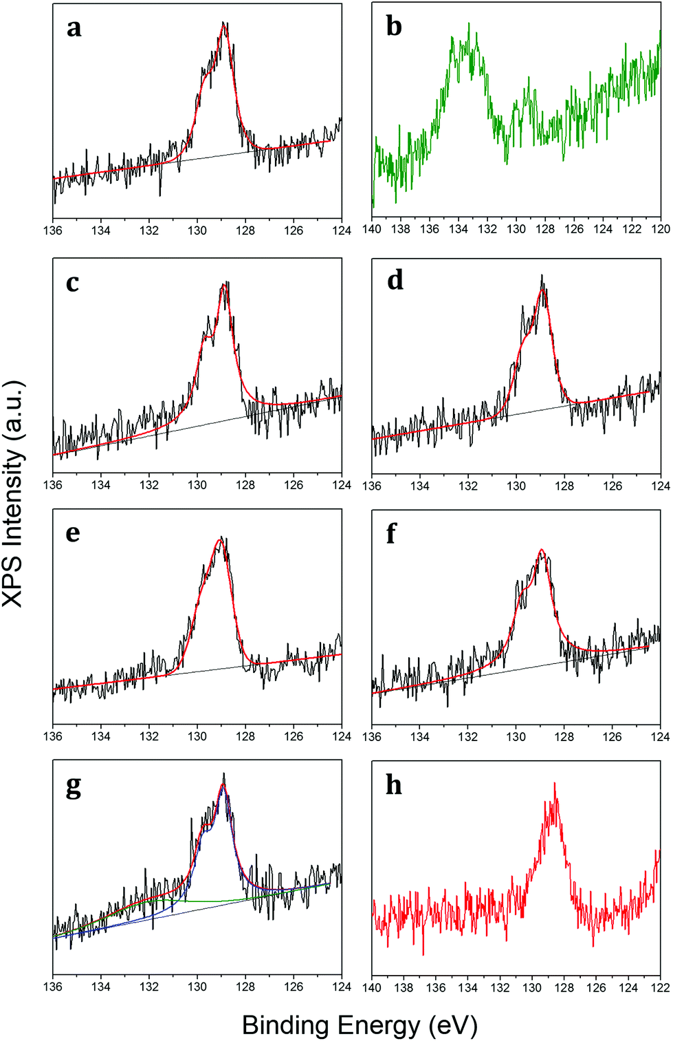 | ||
| Fig. 2 XPS of the P 2p core level as grown (a), when exposed to air for a time longer than 10 min (b), after 100 L O2 dose (c), after 1000 L O2 (d), after 2000 L O2 (e), after 10000 L O2 (f), after exposure to dry air for 10 min (g), and after the 5 nm-thick Al2O3 capping layer on the as-grown sample (h). For the same spectrum after one-month air exposure of the Al2O3-capped epitaxial phosphorene, see Fig. 3b. For panels (b) and (h), only raw data are reported, otherwise black lines show raw data fitted by red lines. In panel (g) the red line is the overall fit of the green (phosphorus oxide) and blue (elemental epitaxial phosphorene) components. | ||
Although epitaxial phosphorene shows a remarkable resistance against oxidation by molecular oxygen and dry air exposures, probably because the upper phosphorus bonds are chemically saturated by the additional phosphorus adatoms, its deterioration takes place under ambient conditions, i.e. with moisture, for a time longer than 10 min and hampers the ex situ characterization and further exploitation (as shown in Fig. 2b). As already proved for other X-enes, like borophene,31 the chemical reactivity of epitaxial phosphorene is comparatively lower when exposed to pure O2 under UHV conditions than when exposed to air, thus being probably promoted by the atmospheric species, e.g. H2O. Similar to silicene, a suitable non-metallic and optically transparent (in a large part of the electromagnetic spectrum) capping layer is Al2O3.32 Epitaxial phosphorene is protected by the in situ co-deposition of aluminium and molecular oxygen (see the Experimental section). Fig. 2h shows the P 2p core level after the Al2O3 growth and Fig. 3b shows the P 2p core level after one-month of air exposure, with a minor component (green) related to the phosphorus oxide and a major one (blue) related to the elemental bonding of epitaxial phosphorene. We find that a 5 nm-thick Al2O3 capping layer is suitable to durably protect the underlying epitaxial phosphorene, as evidenced by a comparison between Fig. 2b and 3b, whereas lower thicknesses, e.g. 2.5 nm (Fig. S6 in the ESI†), are inadequate. Hitherto, the effectiveness of the amorphous Al2O3 capping layer at durably protecting X-enes has been demonstrated only for silicene on Ag(111)32 and on Al2O3(0001).33 This additional proof on epitaxial phosphorene encapsulation thus suggests Al2O3 is a versatile and nearly universal capping layer for the X-enes.
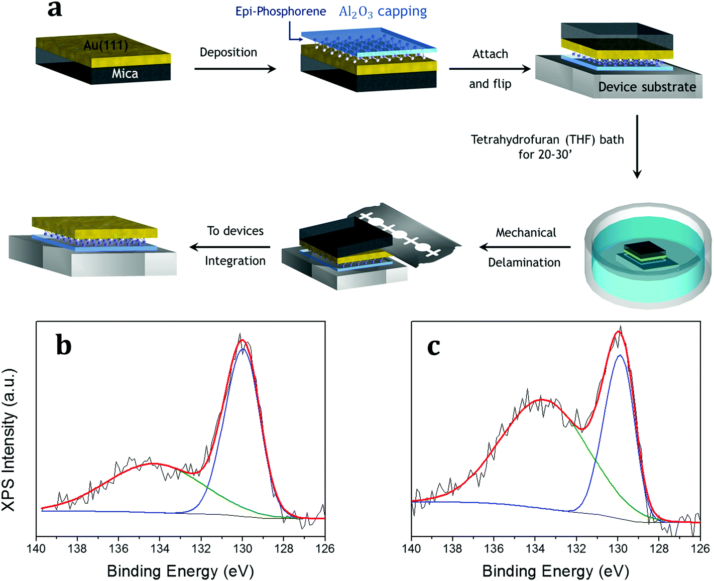 | ||
| Fig. 3 UXEDO process applied to epitaxial phosphorene, which includes the following key steps: epitaxial growth of phosphorene on an Au(111) thin film, in situ Al2O3 capping, overturn of the stacking onto a device-friendly substrate, THF bath for 20–30 min, delamination of the supporting mica, and the transfer of the resulting thin membrane (a), XPS of the P 2p core level before (b) and after (c) the THF bath showing raw data (black), overall fit (red), and single components related to major epitaxial phosphorene (blue) and minor oxidized phosphorus (green). | ||
Epitaxial phosphorene is thus sandwiched in between two protective films, i.e. the Al2O3 capping layer on top and the thin gold layer at the bottom, mechanically supported by mica. Large scale growth and encapsulation are therefore the first stage of the UXEDO process applied to epitaxial phosphorene. Such a configuration can be handled by removing the mica template in an intermediate stage of the UXEDO process. Fig. 3a shows these intermediate steps of the UXEDO process with particular attention to the mica removal. When taken out of the UHV environment, the encapsulated epitaxial phosphorene is accommodated onto a device-friendly SiO2/Si substrate by facing the Al2O3-phosphorene-Au/mica stacking downwards. The reversed stacking is then dipped in a tetrahydrofuran (THF) bath for 20–30 min and then rinsed with deionized water in order to remove the pristine mica layer.
At variance with the SEDNE process, that uses mechanical delamination with a two-tape method to separate the Al2O3-silicene-Ag stack from the mica substrate,6,8 with some unavoidable mica residues remaining in certain areas, the use of THF completely separates mica from the gold thin film allowing for a comparatively larger scale transfer than in the case of silver.6,34 This allows one to easily remove the mica layers from the gold thin film using a cutter without any hint of residual mica (as demonstrated by Raman spectroscopy, see Fig. S7 in the ESI†). The wet delamination process is based on the chemical infiltration of the solvent in between the gold and mica layers, therefore it is barely influenced by the specific details of the mica substrate (that can vary significantly in the same substrate batch, for example, in terms of thickness and the number of mica layers). As a result, the process is characterized by a higher degree of reliability compared to a pure mechanical delamination. On the other hand, the use of a wet transfer methodology instead of a dry one leads to an increase of the partial oxidation of the phosphorene (due to one-month of air exposure), but the main component related to the elemental P 2p core level (blue curve) still survives as demonstrated by the XPS comparison reported in Fig. 3b and c. Unlike graphene and other stable 2D materials, substrate etching based on wet transfer methods cannot be readily extended to the X-enes because of their higher chemical reactivity under ambient conditions.6 Hitherto this is the first case of a wet transfer method applied to an X-ene that shows the survival of the epitaxial phosphorene. Hence, the UXEDO process proves to be a viable methodology to protect and transfer the epitaxial phosphorene, like silicene.
Conclusions
We demonstrate the metastable nature of newly discovered epitaxial phosphorene with a quasi-bilayer (termed adatom-rich) structure due to the saturation of upper-phosphorus bonds. We succeeded in synthesizing semiconductive epitaxial phosphorene with a limited reactivity to molecular oxygen dosing in a vacuum on a large scale thin gold film. To bypass degradation under environmental conditions, we developed a transfer process including top and bottom protective layers, such as Au(111)/mica and amorphous Al2O3 allowing for easy transfer of the epitaxial phosphorene in a chemically protected environment resulting in a thin membrane. These process steps thus look very promising for its forthcoming integration into a device and, most importantly, demonstrate the universal and versatile character of the proposed UXEDO process.Experimental
Sample preparation
Experiments were carried out in a UHV (base pressure 10−10 mbar) system equipped with three interconnected chambers for sample growth via MBE, chemical analysis via XPS, and morphological characterization via STM. Clean ∼300 nm Au(111)/mica substrates were prepared by repeated Ar+ bombardment (1 kV, 1 × 10⁻⁶ mbar) and subsequent annealing at 500 °C for 30 min. Phosphorus was deposited by evaporation from a crucible containing bulk black phosphorus. During the deposition process, the substrate temperature was kept in between 240 and 270 °C. The temperature readings were crosschecked by pyrometer-based calibration of the thermocouple attached under the sample holder. An Al2O3 capping layer is grown in situ by co-deposition of an aluminium beam from a k-cell and ultra-pure molecular oxygen as reported in ref. 32. The Al2O3 thickness is measured ex situ via atomic force microscopy.STM and XPS measurements
STM images were acquired at room temperature with a homemade tungsten tip pre-calibrated onto a HOPG surface. STM topographies were typically acquired at −1.3 V and 0.4 nA setpoint. XPS measurements have been carried out either in situ with nonmonochromatized Mg and Al Kα sources (1253.6 and 1486.6 eV, respectively) at a take-off angle of 37° or ex situ with a monochromatized Al Kα source at a take-off angle of 30°.UXEDO process
The Al2O3-phosphorene-Au(111)/mica samples were attached face down onto clean SiO2/Si substrates, i.e. the Al2O3 side in contact with the SiO2 substrate. The samples were soaked in a THF bath for 20–30 min, then rinsed with deionized water and finally dried with a nitrogen flux. Detachment of the mica substrates was obtained by inserting a blade at the edge of the Au(111)/mica interface. In this way the complete detachment of the mica substrate is accomplished with a complete transfer of the Al2O3-phosphorene-Au(111) membrane. The removal of the mica substrate was demonstrated by using a Renishaw Invia Raman spectrometer (in backscattering configuration) equipped with the 633 nm line of a He–Ne laser focused onto the sample through a 100× objective (0.9 numerical aperture).Conflicts of interest
There are no conflicts to declare.Acknowledgements
The authors acknowledge Mario Alia (CNR-IMM) for technical support and funding support from H2020 ERC CoG 2017 Grant No. 772261 “XFab” and from Fondazione CARIPLO – Regione Lombardia for the project “Crystel”, grant no. 2016-0978.Notes and references
- A. Molle, J. Goldberger, M. Houssa, Y. Xu, S. C. Zhang and D. Akinwande, Nat. Mater., 2017, 16, 163–169 CrossRef CAS PubMed.
- M. Chhowalla, D. Jena and H. Zhang, Nat. Rev. Mater., 2016, 1, 16052 CrossRef CAS.
- D. Akinwande, N. Petrone and J. Hone, Nat. Commun., 2014, 5, 5678 CrossRef CAS PubMed.
- A. J. Mannix, B. Kiraly, M. C. Hersam and N. P. Guisinger, Nat. Rev. Chem., 2017, 1, 0014 CrossRef CAS.
- M. Pumera and Z. Sofer, Adv. Mater., 2017, 29, 1605299 CrossRef PubMed.
- A. Molle, C. Grazianetti, L. Tao, D. Taneja, M. H. Alam and D. Akinwande, Chem. Soc. Rev., 2018, 47, 6370–6387 RSC.
- P. Vogt, P. De Padova, C. Quaresima, J. Avila, E. Frantzeskakis, M. C. Asensio, A. Resta, B. Ealet and G. Le Lay, Phys. Rev. Lett., 2012, 108, 155501 CrossRef PubMed.
- L. Tao, E. Cinquanta, D. Chiappe, C. Grazianetti, M. Fanciulli, M. Dubey, A. Molle and D. Akinwande, Nat. Nanotechnol., 2015, 10, 227–231 CrossRef CAS PubMed.
- C. Grazianetti, E. Cinquanta, L. Tao, P. De Padova, C. Quaresima, C. Ottaviani, D. Akinwande and A. Molle, ACS Nano, 2017, 11, 3376–3382 CrossRef CAS PubMed.
- P. W. Bridgman, J. Am. Chem. Soc., 1914, 36, 1344–1363 CrossRef CAS.
- X. Ling, H. Wang, S. Huang, F. Xia and M. S. Dresselhaus, Proc. Natl. Acad. Sci. U. S. A., 2015, 112, 201416581 Search PubMed.
- H. Thurn and H. Kerbs, Angew. Chem., Int. Ed. Engl., 1966, 5, 1047–1048 CrossRef CAS.
- R. Hultgren, N. S. Gingrich and B. E. Warren, J. Chem. Phys., 1935, 3, 351–355 CrossRef CAS.
- F. Bachhuber, J. von Appen, R. Dronskowski, P. Schmidt, T. Nilges, A. Pfitzner and R. Weihrich, Angew. Chem., Int. Ed., 2014, 53, 11629–11633 CrossRef CAS PubMed.
- H. Okudera, R. E. Dinnebier and A. Simon, Z. Kristallogr. - Cryst. Mater., 2005, 220, 259–264 CAS.
- L. Li, Y. Yu, G. J. Ye, Q. Ge, X. Ou, H. Wu, D. Feng, X. H. Chen and Y. Zhang, Nat. Nanotechnol., 2014, 9, 372–377 CrossRef CAS PubMed.
- H. Liu, A. T. Neal, Z. Zhu, Z. Luo, X. Xu, D. Tománek and P. D. Ye, ACS Nano, 2014, 8, 4033–4041 CrossRef CAS PubMed.
- F. Xia, H. Wang and Y. Jia, Nat. Commun., 2014, 5, 4458 CrossRef CAS PubMed.
- W. Lu, X. Ma, Z. Fei, J. Zhou, Z. Zhang, C. Jin and Z. Zhang, Appl. Phys. Lett., 2015, 107, 021906 CrossRef.
- M. Buscema, D. J. Groenendijk, S. I. Blanter, G. A. Steele, H. S. J. van der Zant and A. Castellanos-Gomez, Nano Lett., 2014, 14, 3347–3352 CrossRef CAS PubMed.
- Z. Zhu and D. Tománek, Phys. Rev. Lett., 2014, 112, 176802 CrossRef PubMed.
- C. Grazianetti, E. Cinquanta and A. Molle, 2D Mater., 2016, 3, 012001 CrossRef.
- J. L. Zhang, S. Zhao, C. Han, Z. Wang, S. Zhong, S. Sun, R. Guo, X. Zhou, C. D. Gu, K. Di Yuan, Z. Li and W. Chen, Nano Lett., 2016, 16, 4903–4908 CrossRef CAS PubMed.
- E. Golias, M. Krivenkov, A. Varykhalov, J. Sánchez-Barriga and O. Rader, Nano Lett., 2018, 18, 6672–6678 CrossRef CAS PubMed.
- J. Zhuang, C. Liu, Q. Gao, Y. Liu, H. Feng, X. Xu, J. Wang, J. Zhao, S. X. Dou, Z. Hu and Y. Du, ACS Nano, 2018, 12, 5059–5065 CrossRef CAS PubMed.
- W. Zhang, H. Enriquez, Y. Tong, A. Bendounan, A. Kara, A. P. Seitsonen, A. J. Mayne, G. Dujardin and H. Oughaddou, Small, 2018, 14, 1804066 CrossRef PubMed.
- N. Han, N. Gao and J. Zhao, J. Phys. Chem. C, 2017, 121, 17893–17899 CrossRef CAS.
- M. T. Edmonds, A. Tadich, A. Carvalho, A. Ziletti, K. M. O'Donnell, S. P. Koenig, D. F. Coker, B. Özyilmaz, A. H. C. Neto and M. S. Fuhrer, ACS Appl. Mater. Interfaces, 2015, 7, 14557–14562 CrossRef CAS PubMed.
- A. I. Kovalev, D. L. Wainstein, D. I. Tetelbaum, W. Hornig and Y. N. Kucherehko, Surf. Interface Anal., 2004, 36, 959–962 CrossRef CAS.
- T. Yang, B. Dong, J. Wang, Z. Zhang, J. Guan, K. Kuntz, S. C. Warren and D. Tománek, Phys. Rev. B: Condens. Matter Mater. Phys., 2015, 92, 125412 CrossRef.
- A. J. Mannix, Z. Zhang, N. P. Guisinger, B. I. Yakobson and M. C. Hersam, Nat. Nanotechnol., 2018, 13, 444–450 CrossRef CAS PubMed.
- A. Molle, C. Grazianetti, D. Chiappe, E. Cinquanta, E. Cianci, G. Tallarida and M. Fanciulli, Adv. Funct. Mater., 2013, 23, 4340–4344 CrossRef CAS.
- C. Grazianetti, S. De Rosa, C. Martella, P. Targa, D. Codegoni, P. Gori, O. Pulci, A. Molle and S. Lupi, Nano Lett., 2018, 18, 7124–7132 CrossRef CAS PubMed.
- M. Hegner, P. Wagner and G. Semenza, Surf. Sci., 1993, 291, 39–46 CrossRef CAS.
Footnote |
| † Electronic supplementary information (ESI) available. See DOI: 10.1039/c9nr06037e |
| This journal is © The Royal Society of Chemistry 2019 |