
 Open Access Article
 This Open Access Article is licensed under a Creative Commons Attribution-Non Commercial 3.0 Unported Licence
Phonon transport across crystal-phase interfaces and twin boundaries in semiconducting nanowires†
Jesús
Carrete‡
 a,
Miquel
López-Suárez‡
b,
Martí
Raya-Moreno
c,
Anton S.
Bochkarev
d,
Miquel
Royo
b,
Georg K. H.
Madsen
a,
Xavier
Cartoixà
c,
Natalio
Mingo
d and
Riccardo
Rurali
*b
a,
Miquel
López-Suárez‡
b,
Martí
Raya-Moreno
c,
Anton S.
Bochkarev
d,
Miquel
Royo
b,
Georg K. H.
Madsen
a,
Xavier
Cartoixà
c,
Natalio
Mingo
d and
Riccardo
Rurali
*b
aInstitute of Materials Chemistry, TU Wien, A-1060 Vienna, Austria
bInstitut de Ciència de Materials de Barcelona (ICMAB–CSIC), Campus de Bellaterra, 08193 Bellaterra, Barcelona, Spain. E-mail: rrurali@icmab.es
cDepartament d'Enginyeria Electrònica, Universitat Autònoma de Barcelona, 08193 Bellaterra, Barcelona, Spain
dCEA, LITEN, 17 Rue des Martyrs, 38054 Grenoble, France
First published on 12th August 2019
Abstract
We combine state-of-the-art Green's-function methods and nonequilibrium molecular dynamics calculations to study phonon transport across the unconventional interfaces that make up crystal-phase and twinning superlattices in nanowires. We focus on two of their most paradigmatic building blocks: cubic (diamond/zinc blende) and hexagonal (lonsdaleite/wurtzite) polytypes of the same group-IV or III–V material. Specifically, we consider InP, GaP and Si, and both the twin boundaries between rotated cubic segments and the crystal-phase boundaries between different phases. We reveal the atomic-scale mechanisms that give rise to phonon scattering in these interfaces, quantify their thermal boundary resistance and illustrate the failure of common phenomenological models in predicting those features. In particular, we show that twin boundaries have a small but finite interface thermal resistance that can only be understood in terms of a fully atomistic picture.
Recent advances in nanowire (NW) growth have provided access to many crystal phases of semiconductor compounds that either are precluded in bulk form or require extreme temperature and pressure conditions to become stable.1 The high degree of control of the growth parameters that favor one polytype over another allows creating homojunctions, most often between a zinc blende (ZB) and a wurtzite (WZ) crystal. These homojunctions form the basis of crystal-phase superlattices, a novel type of structure where different crystal phases of the same material, rather than different materials, are alternated with a given periodicity.2,3 An even subtler type of homojunction is the twin boundary, which results from a 60° rotation of part of the ZB crystal structure that, when arranged periodically, gives rise to the so-called twinning superlattices.4,5 These homojunctions are special in several aspects: (i) they are atomically flat and do not exhibit roughness, (ii) they are defect-free, (iii) their lattice mismatch is very small, and (iv) they cannot feature any chemical intermixing. Therefore, there is a fundamental interest in the properties of these novel interfaces, particularly concerning the role they play in transport phenomena.
Phonons are scattered at the interface between two different materials, giving rise to the phenomenon of thermal boundary resistance (TBR). The TBR is due to the breakdown of translational symmetry by the interface, and the difference in the mass of the constituent atomic species plays a prominent role. Accordingly, one would expect that phonons could pass through a crystal-phase interface, where the atomic mass does not vary, without being scattered. On the other hand, it has been recently shown that the thermal conductivity can decrease by as much as 40% from a cubic to a hexagonal polytype of the same material.6–8 Therefore, there is a need for detailed insight from atomistic calculations of heat transport across homojunctions and of their TBR. Understanding heat transport in these systems is important both for fundamental reasons and with a view to applications.9,10 On the one hand, phonon scattering at crystal-phase interfaces and, particularly, twin boundaries defies many phenomenological models used to account for interface thermal resistance; on the other hand, crystal-phase engineering can be used to design materials with tailor-made properties3,11–15 and twinning superlattices are playing an increasingly important role in nanowire science.16–19
In this work we use both state-of-the-art nonequilibrium Green's functions (NEGF) and nonequilibrium molecular dynamics (NEMD), based on carefully parameterized interatomic potentials, to calculate the TBR of a few prototypical homojunctions, compare them with the values obtained in similar, conventional heterojunctions and elucidate the atomic-scale mechanisms that originate interface scattering. These computational techniques provide complementary information: while NEGF accounts for the quantum nature of phonons in the low to mid temperature regime, NEMD naturally accounts for anharmonicity at all orders, which becomes more important at high temperature.
Computational methods
Ab initio calculations based on density functional theory (DFT) have demonstrated their predictive power in many areas of condensed matter physics,20 including the vibrational and thermal properties of materials.21,22 Nevertheless, because of the high computational load involved, sometimes their use is not practical. This is often the case for the calculation of the interatomic force constants (IFCs) needed to obtain the phonon dispersion and the thermal conductivity in systems featuring an interface, which normally need large simulation cells for their description. Lattice properties can also be computed using computationally lighter, but still reliable methods, such as carefully parameterized interatomic potentials.23,24 A common drawback of these methods, however, is their limited transferability, and their use in a different environment from the one used for the parameterization is in principle questionable. Polytypism is a textbook case in this sense, and indeed it is not guaranteed that a potential parameterized to reproduce the properties of a ZB semiconductor works equally well with the WZ crystal.To address this concern in binary semiconductors, in this article we use a many-body interatomic potential that builds on the previous work of Vashishta and coworkers,25,26 and whose parameterization for GaP27 and InP28 reproduces the properties of different crystal phases, including ZB, WZ, and rock salt. As we are mostly interested in the vibrational properties, we calculated the phonon dispersions of the ZB and WZ crystals and compared them with those obtained by first-principles DFT calculations. We found that the ZB and the WZ phase of both GaP and InP are indeed described to a similar level of accuracy. Acoustic branches, whose accuracy is important in the study of interface or dislocation scattering,29 are reasonably well reproduced (see ESI†). There is a certain overestimation of the group velocity of the transverse modes in the case of GaP and InP, but it is similar for both polytypes.
In contrast, common interatomic force fields for Si, such as the Tersoff30 or the Stillinger–Weber potentials,31 give a rather poor description of vibrational properties.29 Therefore, we used machine-learning techniques to build a neural-network (NN) potential for Si that enables phonon dispersions with ab initio quality for both the cubic diamond (3C) and the hexagonal diamond (lonsdaleite, 2H) polytypes. The energy of the system is expressed as a sum of contributions from the environments of the different atoms,  . An atom's environment is defined by the collection of distances, {rij}, between atom i and its neighbors, up to a cutoff radius rc. This collection of distances is transformed into an array of descriptors,
 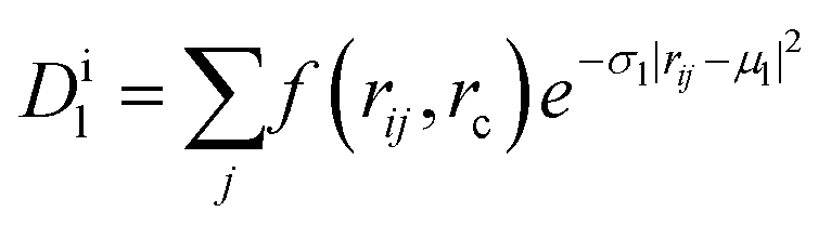 , for the environment of each atom i, where (μl, σl) are adjustable parameters for each member l of the array, and
 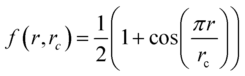 is a smooth cutoff function. The contribution Ei is given by a neural network that has Dil as inputs, and the forces
  on each atom k are the anaytical derivatives of E with respect to atom k's coordinates. The network weights, as well as the sets of parameters (μl, σl), are adjusted to minimize a cost function,
 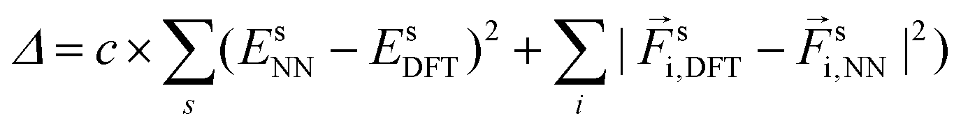 , of the differences between the network- and DFT-calculated energies and forces of all the training systems, s. This minimization is performed by stochastic gradient descent and backpropagation using tensorflow's32 GPU implementation. We used 32 different values of μ and α, and neural network with 2 hidden layers, i.e. 3 layers of coefficients, with 200 and 100 units, c = 0.01, obtaining a RMSE of 0.05 eV Å−1 for forces and 1.3 meV per atom for energies.
Even in the presence of a periodic reconstruction, two discrete translation symmetries can be identified along directions parallel to an interface between two crystalline regions. Therefore, elastic scattering of phonons at the interface is subject to the conservation of a two-dimensional parallel momentum q∥. The problem of heat-carrier reflection and transmission by an interface can thus be decoupled into an infinite set of one-dimensional scattering problems, one for each possible value of q∥ in a two-dimensional parallel Brillouin zone, BZ∥. The full solution to each of those problems consists in obtaining the detailed transmission probabilities per unit time among phonon modes on the left- and right-hand sides of the interface, constrained by the conservation of energy. For instance, for a mode incident upon the interface from the left lead with parallel and perpendicular components of the momentum (q∥, q⊥) and angular frequency ω, one first has to search for all the phonon modes in the left and the right sides compatible with both q∥ and ω, and then calculate the amplitude of each allowed scattering process. This involves exploring an effective one-dimensional Brillouin zone BZ⊥(q∥), looking for values of q⊥ and phonon branch indices yielding the same frequency as the incident phonon. The main difference with respect to a typical one-dimensional problem involving scattering by a barrier is the lack of time-reversal symmetry, which only applies to the line crossing the Γ point.
The detailed procedure described above is computationally expensive and has a tendency to numerical instability because of the need to solve the inverse problem of finding wave vectors as functions of frequency. Therefore, an alternative approach is often used, both in actual one-dimensional thermal transport problems and for interfaces: computing the total phonon transmission at each frequency as the trace of a matrix product, which is independent from the basis used for the wave functions. An example of such approach is the Caroli (or three-region) formula. The phonon transmission is enough to calculate the total thermal conductance in the Landauer–Büttiker formalism and can be used to implement semi-detailed interface scattering in the context of device simulations.33 However, it does not contain enough information to understand how phonon modes at either side are connected to one another. Fortunately, a systematic approach to the full calculation has emerged in recent years,34 which we implemented and used for the present work. In this method, the phonon modes in the leads at a given frequency are extracted from the solutions to ordinary eigenvalue problems for the so-called Bloch matrices, each of which is defined as the product of a Green's function times a hopping IFC matrix, i.e., the IFC block connecting adjacent segments of the leads. The group velocities and transmission are then computed through further matrix operations, and the propagating character of each mode is only analyzed once, so that inconsistencies between different steps of the calculation are avoided.34
We consider the transport direction to be the cubic [111] crystal axis, parallel to the hexagonal [0001] axis, and hence the layer stacking order goes from ABCABC in the ZB to ABABAB in the WZ. This crystallographic axis corresponds to the growth orientation of NWs featuring crystal-phase junctions and twin boundaries reported in the experiments. We take the z axis as perpendicular to the interface and therefore parallel to the transport direction. We study bulk junctions as an effective model of NWs with realistic diameters, which have bulk-like phonon dispersions. Phonon scattering by the sidewalls of the NW, which to a first approximation is independent on the interface scattering that we study here, is thus not explicitly considered.
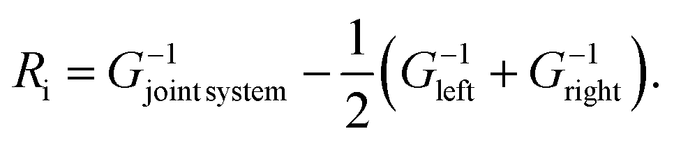
The general workflow, in the transport geometry described above, is as follows. We obtain a full set of harmonic IFCs for a supercell containing two mirror copies of the interface with the Phonopy code.35 The supercell is long enough that interactions between those two copies are negligible, and the regions in between far from the interfaces can be taken as models for the bulk leads. From this set we extract all the IFC submatrices required to describe the harmonic interactions between the scattering regions and the leads, as well as the on-site and hopping matrices of the infinite leads themselves. We enforce the acoustic sum rules on these constants using a Lagrange-multiplier approach to eliminate spurious numerical effects and strictly enforce the short-sighted character of the interactions in this picture. The next step is to sample the two-dimensional BZ of parallel wave vectors using a 61 × 61 regular grid. For each q∥ we apply the procedure described in ref. 34. The ingredients are the effective complex IFCs computed by Fourier-transforming the real-space IFCs along the parallel directions for that value of q∥, the Green's function of the scattering region obtained by direct inversion, and the surface Green's functions of the leads calculated by a real-space renormalization-group method, decimation.36,37 With those ingredients we obtain the mode-by-mode energy transmission coefficients between phonons at both sides of the interface34 and, by summing over channels, the total phonon transmission for a particular q∥. An average over the two-dimensional parallel BZ is required to compute the total transmission determining the thermal conductance. The final step is to isolate the effect of the interface, whose thermal resistance per unit area is extracted using the standard approach of subtracting the contribution of the leads:
 | (1) |
The thermal conductances in eqn (1) are computed using the Landauer formula38,39 as
 | (2) |
We also perform NEMD calculations on GaP and InP boxes containing a crystal-phase interface that separates a ZB and a WZ segment of 40 nm each with the LAMMPS code.40 After an initial structural relaxation with a standard conjugate gradient algorithm we connect the ends of the computational cell to two Nosé–Hoover thermostats set at a hot and a cold temperature, TH and TC. We then evaluate the resulting heat flux from the work done by the thermostats.41,42 The total simulation time is 2.5 ns and we use a timestep of 1 fs. The heat flux and temperature are averaged over the last nanosecond, after checking that the system reached the nonequilibrium steady state prior to that. The temperature as a function of position, T(z), is computed as 2Ek/(3kB), where Ek is the average kinetic energy per atom within a slice of thickness δz of the computational cell. The TBR is calculated as the ratio between the temperature discontinuity across the interface (ΔT) and the heat current through it (J), as well as with the nonequilibrium thermodynamics formalism of ref. 43; the two approaches yield values in good agreement. We use a fixed ΔT = TH − TC of 100 K, similarly to other NEMD calculations,42,44,45 but vary TH and TC in order to sample different interface temperatures.
Crystal-phase interfaces in GaP and InP
Our first target systems are crystal-phase junctions in GaP and InP. In Fig. 1 we plot the phonon transmission,![[scr T, script letter T]](https://www.rsc.org/images/entities/char_e533.gif) (E), as a function of energy. The side panels show the same magnitude for the leads, i.e., for infinite, unperturbed all-ZB and all-WZ systems. From this energy-resolved result it is already possible to draw the conclusion that the degradation of the transmission induced by the interface is rather moderate in the case of GaP, while it is more sizeable for InP, particularly in the low-frequency part of the spectrum. These considerations are confirmed by the quantitative analysis of the TBR, which we compute from eqn (1) and display in Fig. 1(c). We find an extremely low TBR for the GaP crystal-phase junction, which at room temperature is approximately one order of magnitude smaller than in GaN–AlN46 or Si–Ge heterointerfaces43 (see also Table 1). The InP crystal-phase junction, on the other hand, is considerably more resistive and takes values in the same order of magnitude as those of the GaN–AlN system.
(E), as a function of energy. The side panels show the same magnitude for the leads, i.e., for infinite, unperturbed all-ZB and all-WZ systems. From this energy-resolved result it is already possible to draw the conclusion that the degradation of the transmission induced by the interface is rather moderate in the case of GaP, while it is more sizeable for InP, particularly in the low-frequency part of the spectrum. These considerations are confirmed by the quantitative analysis of the TBR, which we compute from eqn (1) and display in Fig. 1(c). We find an extremely low TBR for the GaP crystal-phase junction, which at room temperature is approximately one order of magnitude smaller than in GaN–AlN46 or Si–Ge heterointerfaces43 (see also Table 1). The InP crystal-phase junction, on the other hand, is considerably more resistive and takes values in the same order of magnitude as those of the GaN–AlN system.
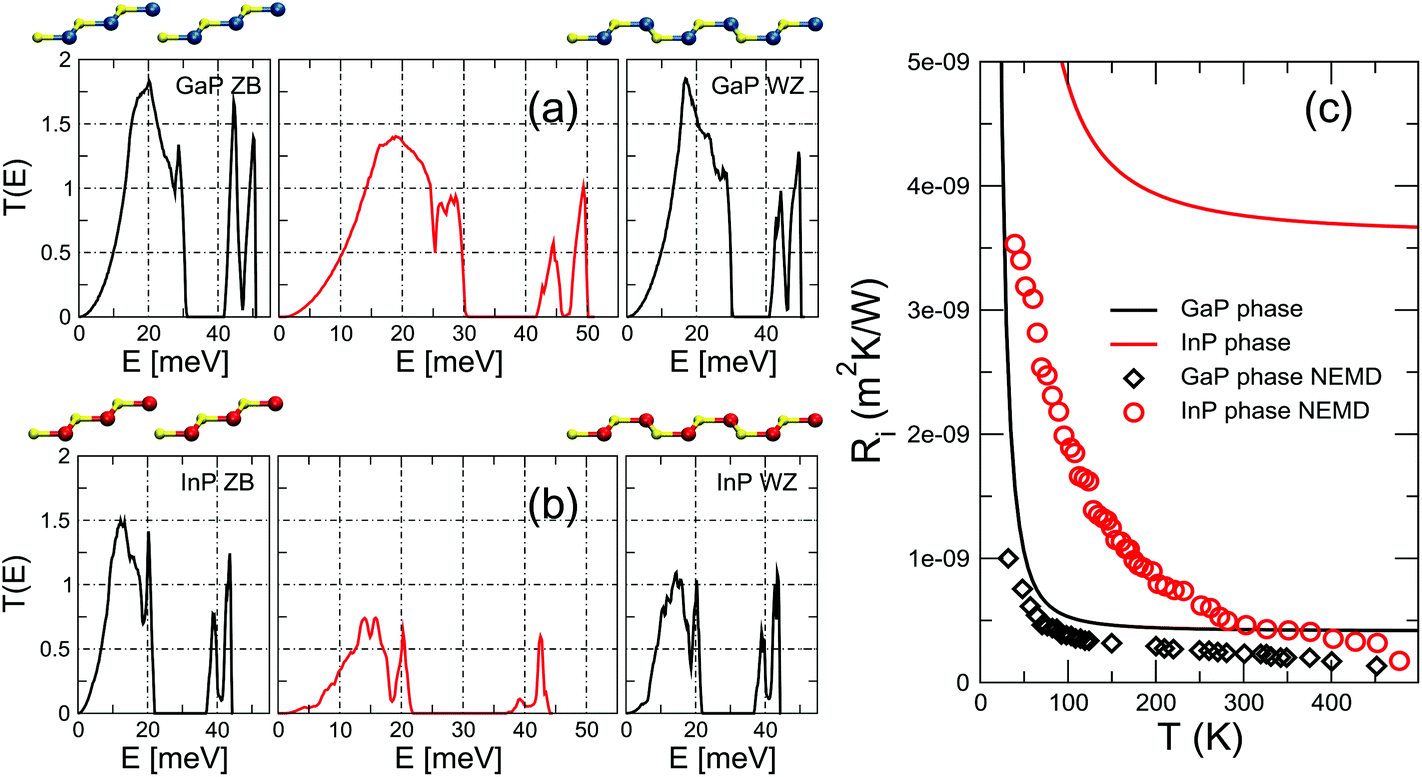 | ||
| Fig. 1 Transmission through a (a) GaP and (b) InP crystal-phase interface. The harmonic transmission functions of the perfect, infinite leads are shown in the side panels. The ball-and-stick models show the change from ABCABC stacking along the [111] cubic axis in the left lead to ABABAB stacking along the [0001] hexagonal axis in the right lead (blue, yellow, and red spheres represent Ga, P, and In atoms). (c) TBR as a function of interface temperature for the two crystal-phase interfaces obtained using the (E) from panels (a) and (b). Data points show the TBR computed from NEMD, which includes anharmonic effects at the interface. The uncertainty in the estimate of the TBR from NEMD, arising from the fluctuating character of the temperature profile, is 9.6 × 10⁻¹¹ m2 K W−1 and 5.9 × 10⁻¹⁰ m2 K W−1 for GaP and InP, respectively. | ||
With the purpose to understand the difference between the two crystal phase interfaces, we analyze the mismatch in vibrational properties between the ZB and the WZ phase of the two materials. In principle, a situation where the (E) of the left and right leads are as similar as possible favors phonon propagation across the interface, since energy can be more easily conserved. To check whether this intuitive fact correlates with the thermal transport results, in Fig. 2 we plot the absolute value of the difference between the transmission of the ZB and the WZ crystal-phase, ZB(E) and WZ(E), for both GaP and InP. As can be seen from looking directly at the curves or at their integrals (depicted in the bottom panel of the same figure), the differences between the ZB and WZ transmissions are mostly concentrated in the low-frequency range in the case of InP. Hence they are indeed expected to result in a larger resistance, since this range is especially critical for thermal transport because of the higher group velocities and lower scattering rates of phonons with such energies. This observation agrees well with the calculated TBR of Fig. 1(c). It is also related to the significantly larger ratio between the thermal conductivities of the cubic and hexagonal phases in InP with respect to GaP, as discussed in detail in ref. 8. Nonetheless, it is already clear that this qualitative analysis will not be applicable to the case of twin boundaries where, no matter the compound, the transmissions of the perfect leads are identical by construction.
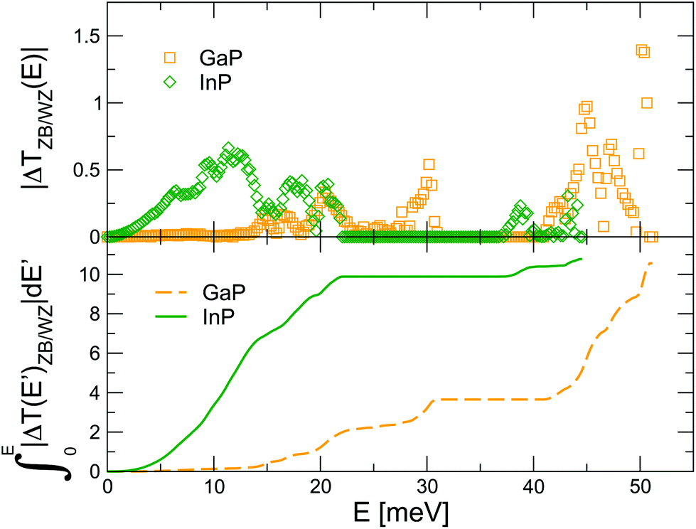 | ||
| Fig. 2 (Top) Absolute value of the difference between the transmission of the ZB and the WZ leads, ΔZB/WZ(E), for GaP and InP plotted in Fig. 1. (Bottom) Definite integral from E = 0 of the differences depicted in the top panel. | ||
Within the NEGF scheme, the interface is described at the harmonic level and phonon–phonon scattering processes are neglected. In a bulk material anharmonicities result in resistive collisions, i.e. Umklapp scattering, and are the main cause for the finite value of the thermal conductivity in solids. For an interface, conversely, anharmonic processes can increase the conductance by opening new transmission channels, analogously to the case of inelastic electron tunneling spectroscopy.47,48 This is easily illustrated considering the limiting case in which the leads have misaligned phonon gaps: a phonon of energy ħω1 of one of the leads cannot be transmitted across the interface if the other lead has no available states at that energy. With anharmonicities in play, on the other hand, three-phonon process such as ħω1 + ħω2 → ħω3 and ħω1 → ħω2 + ħω3 become possible at the interface and increase the probability of transmission. Our NEMD simulations, which naturally account for anharmonicities of all orders, allow us to quantify the influence of the effect just described by comparing the results with the NEGF calculations carried out using the same potentials. It must be kept in mind, however, that within NEMD the atoms move classically following Newton's equations of motion, so in the low-temperature regime where the effects of quantum statistics are relevant these results should only be taken qualitatively.
Such a comparison is presented in Fig. 1(c). The good agreement between NEGF and NEMD for the GaP crystal-phase junction indicates that in this case anharmonicities at the interface do not play an important role and the interface thermal resistance decreases only marginally when they are included. A similar agreement has been recently reported for PbTiO3 domain walls.49 The behavior of the InP crystal-phase interface, on the other hand, is quite different: at T > 300 K we find that the TBR is five times lower than the prediction of the harmonic approximation and of the same order of the one of GaP. The much larger significance of anharmonicity in InP can be probably traced to the higher degree of mismatch between the ZB and WZ phases at the harmonic level in the regions most relevant for thermal transport, as discussed in previous paragraphs based on the results presented in Fig. 2.
Twin boundaries in GaP and InP
Although twin boundaries are known to occur in bulk polycrystalline samples,50–53 their use in the context of NWs, where they can be arranged parallel to each other and with a well defined periodicity4,5 gives rise to very special systems, and a few isolated reports54,55 hint at the possibility to extend such arrangements to bulk systems. Here the crystal phase is the same on the two sides of the interface, but the ZB structure undergoes a rotation of 60° and forms a twin boundary planar defect.We find very low TBRs for both GaP and InP twin interfaces, closely resembling the results obtained for the crystal-phase interface of GaP. Specifically, the values of the TBR at T > 100 K are approximately 5 × 10⁻¹⁰ m2 K W−1 (see Fig. 3). Besides the relevance that they have for applications, the results obtained with the twin interfaces are important because they directly challenge common phenomenological models for the calculation of the TBR such as the acoustic mismatch model (AMM) or the diffuse mismatch model (DMM), either within the Debye approximation56 or in the full-band formalism.57,58 Both of these models derive the TBR from the mismatch of the vibrational properties of the materials involved. In a twin boundary, however, the phonon dispersions on the two sides of the interface are the same. Therefore the AMM would predict a zero TBR, in disagreement with our results, which yield a small, but finite value. Incidentally, we observe that the twin homojunction is the prototype of a flat interface, where the AMM should provide more accurate results. The DMM, on the other hand, would yield a nonzero TBR, but it would have no way to discriminate between a twin interface and a virtual interface with truly zero resistance, i.e., one separating two halves of a fully homogeneous sample considered as different regions. This is a known computational artifact of the DMM.
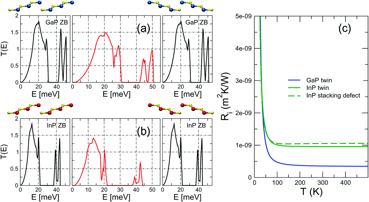 | ||
| Fig. 3 Transmission through a (a) GaP and (b) InP twin boundary interface. The harmonic transmission functions of the perfect, infinite leads are shown in the side panels. The ball-and-stick models show the change from ABCABC to CBACBA stacking along the [111] cubic axis in the left and right leads (blue, yellow, and red spheres represent Ga, P, and In atoms). (c) TBR as a function of interface temperature for the two twin boundary interfaces obtained from the (E) of panels (a) and (b). | ||
For a closer look at the scattering properties of the twin boundary, we have analyzed some local properties of the interface itself. In Fig. 4 we plot the average nearest-neighbor distance, the on-site and the nearest-neighbor harmonic IFCs moving across the interface. As expected, in the case of the crystal-phase interface these magnitudes change from a ZB to a WZ bulk value and the spatial extent of this transition is a good estimate of the thickness of the interface.43,59,60 In the case of the twin boundary the bulk values on either side are the same, but all these magnitudes feature a bump at the interface, an indication of the small, but non-negligible relaxation of the atomic structure. Phase field crystal methods have been shown to be able to capture the effects of a finite interface thickness and of the related strain in semiconductor systems.61 We argue that our results can be used to inform one of such phase field models, which can then be used for computationally lighter simulations.
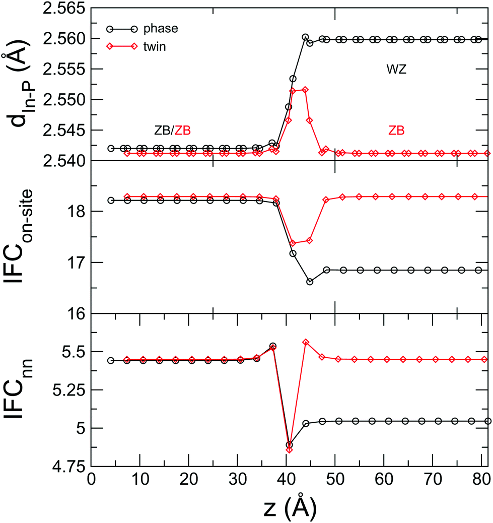 | ||
Fig. 4 (a) Nearest-neighbor distance, (b) on-site IFC and (c) nearest-neighbor IFC as a function of the position along the transport direction for a crystal-phase interface and a twin boundary in InP. The on-site IFC is computed as the Frobenius norm of the Jacobian of the forces of atom m with respect to its own displacement,  , where m is an In atom; similarly, the nearest-neighbor IFC is defined as , where m is an In atom; similarly, the nearest-neighbor IFC is defined as  , where n is a P atom and a first neighbor of m such that zm < zn. , where n is a P atom and a first neighbor of m such that zm < zn. | ||
To get additional insight into the microscopic origin of the thermal resistance at a twin interface, we also analyze the detailed transmission function in twinned InP. There is a clear one-to-one correspondence between phonon modes at both sides, and indeed the overall phonon transmissions of both leads are exactly identical. However, although the 2D Brillouin zones from which q∥ is sampled are equivalent, they are not identical because the respective mode polarization vectors are rotated by a 60° angle. This is well illustrated by Fig. 5(a), where we plot the phonon dispersion of both leads for a specific low-symmetry q∥ value, (qx, qy) = (cos(π/8), sin(π/8)). Since q∥ is conserved in the scattering process, this becomes a one-dimensional scattering problem between effective leads with different phonon spectra due to the rotation of the mode polarizations. The less-than-perfect transmission found for this value of q∥, which we present in Fig. 5(b), is a clear reflection of this fact. If we look at how modes incident on the interface from the left can be transmitted to the right lead, it becomes even more apparent that, even when there is only one vibrational mode available at each side at a particular energy, the coupling between them is far from ideal. To a certain extent this can be understood in terms of the overlap between the rotated phonon polarizations.
 | ||
| Fig. 5 (a) Phonon dispersion of both leads in an InP twin interface and (b) transmission for (qx, qy) = (cos(π/8), sin(π/8)). (c) Detailed transmission for the same q∥: the numbers of rows and columns are equal to the number of modes in each lead at each sampled frequency, annotated in red; the color of each square gives the energy transmission coefficient between each pair of modes according to the color code on the right-hand side. Therefore, and for instance, at E = 1.84 meV there are no propagating modes, at E = 5.53 meV there are two modes on each side with rather low transmission, and at E = 13.82 meV there is a single mode with near ideal transmission. | ||
These two effects –the structural distortion localized at the interface and the rotation of the polarization vectors– are the physical reasons behind the TBR of the twin boundary. It is useful to compare it with the TBR of a simple stacking defect such as ABCABC|AB|ABCABC, i.e. an all-ZB system with a missing layer. In this interface there is no rotation of the polarization vectors between the leads, which are identical, so all the scattering must come only from the local distortion at the interface. The resulting TBR, plotted in Fig. 3 for the case of InP, is slightly larger than the one of the twin boundary, indicating that in this case a larger local distortion (the interface region is thicker than in the twin boundary) can have, on its own, an effect comparable to the more complex scattering at a twin boundary. Indeed, these results are a useful reminder of the fact that, while it is certainly true that homointerfaces are flat and have no chemical intermixing, they do nonetheless have an effective thickness, and that distances between atomic planes (and thus interatomic forces) are altered within a finite, if narrow, spatial region.
Crystal-phase interfaces and twin boundaries in Si
The formation of WZ segments in III–V NWs is today well understood, and is known to be directly correlated to the wetting angle of the catalytic droplet during growth.62 In the case of group-IV semiconductors, on the other hand, the mechanisms are different and interfaces between cubic (3C) and hexagonal (2H) phases have been obtained through shear stress,18,63,64 at NW kinks65,66 or taking advantage of the catalytic properties of magnetite nanocrystals.67 Consequently, the level of control of the positioning of hexagonal segments is considerably lower than what can be achieved in III–V NWs. Nevertheless, isolated and non-periodic cubic–hexagonal interfaces in Si and Ge NWs are observed68 and thus it is interesting to study phonon transport across these interfaces as well. Similar considerations can be made for twin boundaries that have been reported in Si NWs69,70 and that can be positioned with increasingly deterministic precision.71,72The transmission and TBR for a crystal-phase interface between 3C- and 2H-Si and for a twin boundary are shown in Fig. 6. We obtain a remarkably low thermal resistance associated to both the twin boundary and the crystal-phase interface. The values are only slightly lower than those obtained for GaP and InP in previous sections, which can be somewhat surprising given that the additional contribution to interface mismatch coming from the misalignment of polar In/Ga–P bonds is obviously absent in Si. It must be taken into account, however, that the level of ionicity of GaP and InP is relatively low, with those bonds being mostly covalent. The similar values allow us to reasonably speculate that the geometrical mechanism behind the TBR (interfacial readjustment and rotation of the 2D Brillouin zone plus the polarization vectors) have a certain degree of universality.
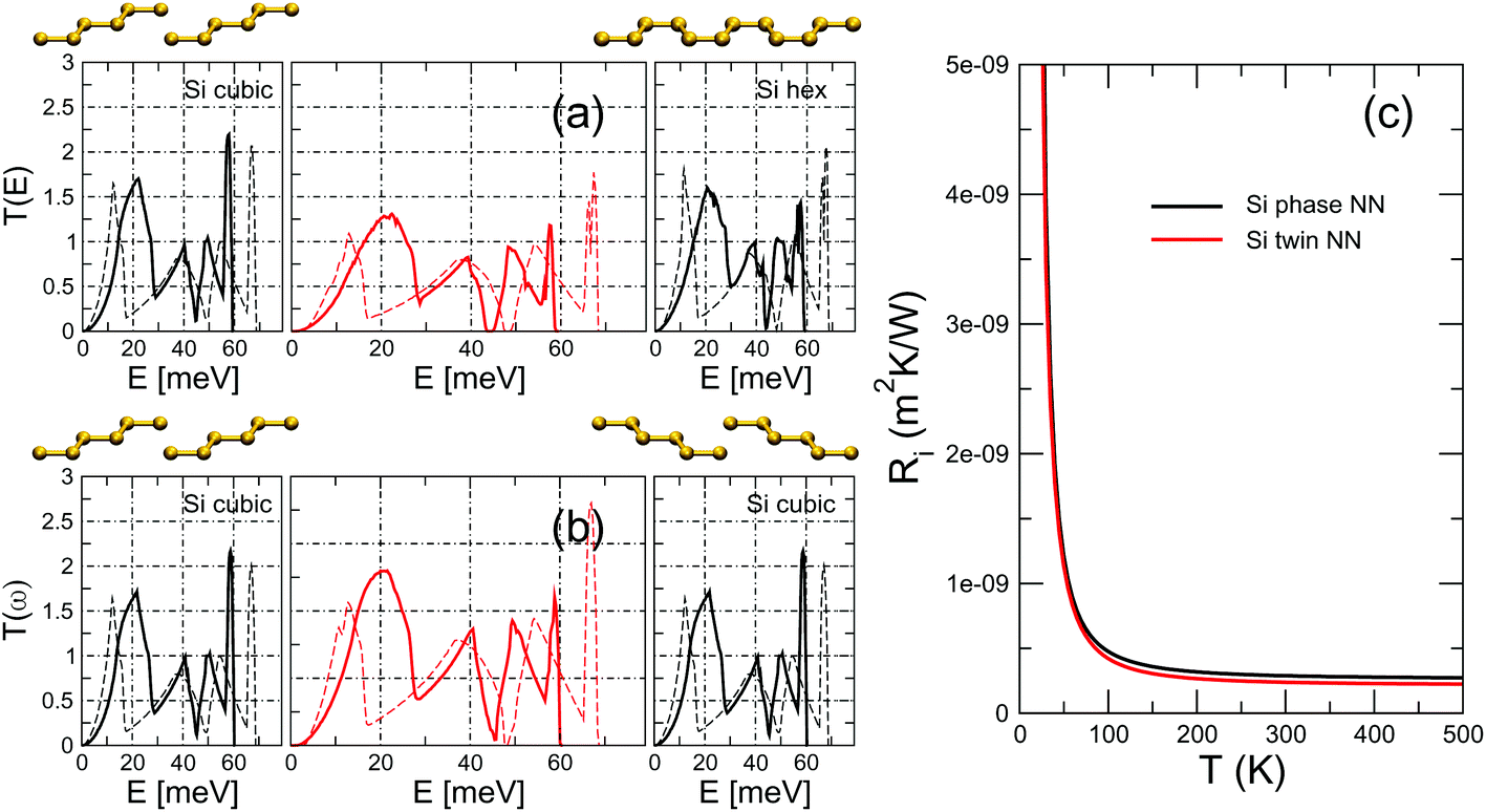 | ||
| Fig. 6 Transmission through a Si (a) phase and (b) twin boundary interface. The harmonic transmission functions of the perfect, infinite leads are shown in the side panels. The ball-and-stick models show the change from ABCABC to CBACBA stacking along the [111] cubic axis in the transition from the left to the right lead. We plot the results obtained with both the optimized NN potential (continuous lines), that yields phonon dispersions with ab initio accuracy, and the Tersoff potential (dashedlines). (c) TBR as a function of interface temperature for the two interfaces obtained from the NN-potential results for (E) of panels (a) and (b). | ||
These results have been obtained with a carefully optimized NN potential that gives phonon dispersions in excellent agreement with DFT. For comparison we also calculate (E) and the TBR using the IFCs computed with the Tersoff potential.30 As can be seen, neither the (E) of any of the leads nor that of a system with an interface are well reproduced by the Tersoff potential, which in particular overestimates the phonon bandwidth by as much as 10 meV. These results point to the need of a well tested potential that provides phonon dispersions in good agreement with DFT benchmarks in order to obtain reliable results for the phononic properties. Nevertheless, we note that, due to a cancellation of errors in the three (E), the estimate of the TBR computed from the Tersoff potential is reasonably accurate, reinforcing the idea of some relatively universal geometric effects in play as stated above.
Multiple interfaces and interference effects
The discussion in this paper is formulated in terms of the transmission of a single interface. Multiple interfaces can in principle create interference effects, and it has been speculated that they could constitute the basis for phononic metamaterials with tunable vibrational properties19 and thermal conductivities.73,74 Although an exhaustive study of crystal-phase and twinning superlattices is beyond the scope of this work, as a test on the method we have examined the interference effects in a double-interface setting. To this end, we have considered phonon transport across two twin boundaries separated by 27 In–P layers (∼9 nm) and in Fig. 7 we plot the transmission(E) of this double barrier for the same q∥ of Fig. 5. In the same figure we also plot the same result for the case of the isolated twin boundary for comparison.
 | ||
| Fig. 7 Transmission through single and double InP twin boundaries for a parallel wave vector of (qx, qy) = (cos(π/8), sin(π/8)). | ||
As can be seen, the addition of a second barrier does not necessarily imply a marked decrease of the transmission. This is a known behavior in the harmonic regime in the limit of large reflection coefficients: if a phonon is efficiently stopped by an interface, adding a second identical interface will not have a marked effect on the overall transmission. More importantly, however, we observe as well that several antiresonances appear throughout the transmission spectrum, an evidence that the two interfaces give rise to destructive interference between the incoming and the reflected waves. These results suggest that if we added more barriers, i.e. twin boundaries, the antiresonances would result in forbidden bandgaps, just like it is observed with heterointerfaces. In other words, on a qualitative level twinning superlattices can behave like conventional superlattices, as also hinted by the NEMD simulations of Porter and coworkers.75
However, these considerations are valid only in the purely coherent and harmonic regime, where it is assumed that phonons retain their coherence while traveling from one interface to the next. As a matter of fact, it has been demonstrated76 that, as far as thermal transport is concerned, phonon scattering by different periods of a superlattice can be treated as incoherent. This assertion is strongly supported by the accuracy and predictive value afforded by calculations based on that hypothesis. Moreover, regarding forbidden regions, the realization of phononic metamaterials for thermal transport applications is hindered by the extremely long wavelength of the relevant phonons. Whether twinning superlattices can mitigate these effects is still an open question. Thus, we argue that a more realistic description of heat transport in twinning superlattices with multiple interfaces calls for a theoretical approach where phonons are scattered elastically at the interfaces, according to the detailed transmission discussed in this work, and predominantly inelastically in between.33 Experimental measurements will also be crucial to shed light on these issues.
Conclusions
In summary, we have carried out an atomistic theoretical study of phonon scattering at crystal-phase interfaces and twin boundaries, both of which are commonly observed in NWs and constitute the building blocks for crystal-phase and twinning superlattices, respectively. We have computed and analyzed the TBR showing that (i) in twin boundaries it is much lower than in typical (i.e. heterogeneous) semiconductor interfaces; (ii) in crystal-phase interfaces it can be as low as in twin boundaries, but in general it depends on the mismatch between the phonon dispersions of the two polytypes involved and anharmonicity can lower it at higher temperatures; (iii) in the elusive case of the twin boundary, it originates from a combined effect of the local structural distortion at the interface and the rotation of the polarization vectors. We have showed that phenomenological models often used to estimate the TBR cannot provide a description of scattering in these subtle interfaces, not even at a qualitative level. Finally, we have discussed the implications for superlattices, showing that nothing prevents homointerfaces to host wave interference effects similarly to those predicted in heterointerfaces.Conflicts of interest
There are no conflicts to declare.Acknowledgements
We acknowledge financial support by the Ministerio de Economía, Industria y Competitividad (MINECO) under grants FEDER-MAT2017-90024-P, TEC2015-67462-C2-1-R (MINECO/FEDER) and RTI2018-097876-B-C21 (MICINN/FEDER), the Severo Ochoa Centres of Excellence Program under Grant SEV-2015-0496 and by the Generalitat de Catalunya under grants no. 2014 SGR 301 and 2017 SGR 1506. M. L. S. is funded through a Juan de la Cierva fellowship. M. R. M. acknowledges support from FPU2016/02565. We thank J. A. Seijas-Bellido for preliminary tests with the Vashishta potential.References
- P. Caroff, J. Bolinsson and J. Johansson, IEEE J. Sel. Top. Quantum Electron., 2011, 17, 829–846 CAS.
- P. Caroff, K. A. Dick, J. Johansson, M. E. Messing, K. Deppert and L. Samuelson, Nat. Nanotechnol., 2009, 4, 50–55 CrossRef CAS PubMed.
- K. A. Dick, C. Thelander, L. Samuelson and P. Caroff, Nano Lett., 2010, 10, 3494–3499 CrossRef CAS PubMed.
- R. E. Algra, M. A. Verheijen, M. T. Borgström, L.-F. Feiner, G. Immink, W. J. P. van Enckevort, E. Vlieg and E. P. A. M. Bakkers, Nature, 2008, 456, 369–372 CrossRef CAS PubMed.
- T. Burgess, S. Breuer, P. Caroff, J. Wong-Leung, Q. Gao, H. Hoe Tan and C. Jagadish, ACS Nano, 2013, 7, 8105–8114 CrossRef CAS PubMed.
- A. Togo, L. Chaput and I. Tanaka, Phys. Rev. B: Condens. Matter Mater. Phys., 2015, 91, 094306 CrossRef.
- M. Raya-Moreno, H. Aramberri, J. A. Seijas-Bellido, X. Cartoixà and R. Rurali, Appl. Phys. Lett., 2017, 111, 032107 CrossRef.
- M. Raya-Moreno, R. Rurali and X. Cartoixà, 2019, arXiv:1901.03268.
- A. Weathers, A. L. Moore, M. T. Pettes, D. Salta, J. Kim, K. Dick, L. Samuelson, H. Linke, P. Caroff and L. Shi, MRS Proc., 2012, 1404, mrsf11–1404-w04–06 CrossRef.
- D. Majumdar, S. Biswas, T. Ghoshal, J. D. Holmes and A. Singha, ACS Appl. Mater. Interfaces, 2015, 7, 24679–24685 CrossRef CAS PubMed.
- C. Thelander, P. Caroff, S. Plissard, A. W. Dey and K. A. Dick, Nano Lett., 2011, 11, 2424–2429 CrossRef CAS PubMed.
- S. Assali, I. Zardo, S. Plissard, D. Kriegner, M. A. Verheijen, G. Bauer, A. Meijerink, A. Belabbes, F. Bechstedt, J. E. M. Haverkort and E. P. A. M. Bakkers, Nano Lett., 2013, 13, 1559–1563 CrossRef CAS PubMed.
- B. Loitsch, J. Winnerl, G. Grimaldi, J. Wierzbowski, D. Rudolph, S. Morkötter, M. Döblinger, G. Abstreiter, G. Koblmüller and J. J. Finley, Nano Lett., 2015, 15, 7544–7551 CrossRef CAS PubMed.
- M. Amato, T. Kaewmaraya, A. Zobelli, M. Palummo and R. Rurali, Nano Lett., 2016, 16, 5694–5700 CrossRef CAS PubMed.
- X. Cartoixà, M. Palummo, H. I. T. Hauge, E. P. A. M. Bakkers and R. Rurali, Nano Lett., 2017, 17, 4753–4758 CrossRef PubMed.
- I.-J. Chen, S. Lehmann, M. Nilsson, P. Kivisaari, H. Linke, K. A. Dick and C. Thelander, Nano Lett., 2017, 17, 902–908 CrossRef CAS PubMed.
- Y. Qian and Q. Yang, Nano Lett., 2017, 17, 7183–7190 CrossRef CAS PubMed.
- C. Fasolato, M. De Luca, D. Djomani, L. Vincent, C. Renard, G. Di Iorio, V. Paillard, M. Amato, R. Rurali and I. Zardo, Nano Lett., 2018, 18, 7075–7084 CrossRef CAS PubMed.
- M. De Luca, C. Fasolato, M. A. Verheijen, Y. Ren, M. Y. Swinkels, S. Kölling, E. P. A. M. Bakkers, R. Rurali, X. Cartoixà and I. Zardo, Nano Lett., 2019, 19, 4702–4711 CrossRef CAS PubMed.
- R. M. Martin, Electronic structure: basic theory and practical methods, Cambridge Univ. Press, Cambridge, 2004 Search PubMed.
- W. Li, J. Carrete, N. A. Katcho and N. Mingo, Comput. Phys. Commun., 2014, 185, 1747–1758 CrossRef CAS.
- J. Carrete, B. Vermeersch, A. Katre, A. van Roekeghem, T. Wang, G. K. Madsen and N. Mingo, Comput. Phys. Commun., 2017, 220, 351–362 CrossRef CAS.
- D. Frenkel and B. Smit, Understanding Molecular Simulations: From Algorithms to Applications, Academic Press, Inc., 1996 Search PubMed.
- A. Rohskopf, H. R. Seyf, K. Gordiz, T. Tadano and A. Henry, npj Comput. Mater., 2017, 3, 27 CrossRef.
- P. Vashishta, R. K. Kalia, J. P. Rino and I. Ebbsjö, Phys. Rev. B: Condens. Matter Mater. Phys., 1990, 41, 12197–12209 CrossRef CAS PubMed.
- I. Ebbsjö, R. K. Kalia, A. Nakano, J. P. Rino and P. Vashishta, J. Appl. Phys., 2000, 87, 7708–7711 CrossRef.
- C. I. Ribeiro-Silva, J. P. Rino, L. G. V. Gonçalves and A. Picinin, J. Phys.: Condens. Matter, 2011, 23, 055801 CrossRef CAS PubMed.
- P. S. Branicio, J. P. Rino, C. K. Gan and H. Tsuzuki, J. Phys.: Condens. Matter, 2009, 21, 095002 CrossRef PubMed.
- T. Wang, J. Carrete, N. Mingo and G. K. H. Madsen, ACS Appl. Mater. Interfaces, 2019, 11, 8175–8181 CrossRef CAS PubMed.
- J. Tersoff, Phys. Rev. B: Condens. Matter Mater. Phys., 1989, 39, 5566–5568 CrossRef PubMed.
- F. H. Stillinger and T. A. Weber, Phys. Rev. B: Condens. Matter Mater. Phys., 1985, 31, 5262–5271 CrossRef CAS PubMed.
- M. Abadi, et al., TensorFlow: Large-Scale Machine Learning on Heterogeneous Systems, 2015; https://www.tensorflow.org/, Software available from tensorflow.org Search PubMed.
- A. van Roekeghem, B. Vermeersch, J. Carrete and N. Mingo, Phys. Rev. Appl., 2019, 11, 034036 CrossRef CAS.
- Z.-Y. Ong, J. Appl. Phys., 2018, 124, 151101 CrossRef.
- A. Togo and I. Tanaka, Scr. Mater., 2015, 108, 1–5 CrossRef CAS.
- F. Guinea, C. Tejedor, F. Flores and E. Louis, Phys. Rev. B: Condens. Matter Mater. Phys., 1983, 28, 4397–4402 CrossRef CAS.
- W. Zhang, T. S. Fisher and N. Mingo, Numer. Heat Transfer, Part B, 2007, 51, 333–349 CrossRef CAS.
- L. G. C. Rego and G. Kirczenow, Phys. Rev. Lett., 1998, 81, 232–235 CrossRef CAS.
- N. Mingo, Phys. Rev. B: Condens. Matter Mater. Phys., 2006, 74, 125402 CrossRef.
- S. Plimpton, J. Comp. Physiol., 1995, 117, 1–19 CrossRef CAS.
- J. Lee, V. Varshney, A. K. Roy, J. B. Ferguson and B. L. Farmer, Nano Lett., 2012, 12, 3491–3496 CrossRef CAS PubMed.
- R. Rurali, X. Cartoixà and L. Colombo, Phys. Rev. B: Condens. Matter Mater. Phys., 2014, 90, 041408 CrossRef.
- R. Rurali, L. Colombo, X. Cartoixà, O. Wilhelmsen, T. T. Trinh, D. Bedeaux and S. Kjelstrup, Phys. Chem. Chem. Phys., 2016, 18, 13741–13745 RSC.
- P. K. Schelling, S. R. Phillpot and P. Keblinski, Phys. Rev. B: Condens. Matter Mater. Phys., 2002, 65, 144306 CrossRef.
- D. G. Cahill, W. K. Ford, K. E. Goodson, G. D. Mahan, A. Majumdar, H. J. Maris, R. Merlin and S. R. Phillpot, J. Appl. Phys., 2003, 93, 793–818 CrossRef CAS.
- C. A. Polanco and L. Lindsay, Phys. Rev. B, 2019, 99, 075202 CrossRef CAS.
- B. C. Stipe, M. A. Rezaei and W. Ho, Science, 1998, 1732–1735 CrossRef CAS PubMed.
- N. Lorente and M. Persson, Phys. Rev. Lett., 2000, 85, 2997–3000 CrossRef CAS PubMed.
- J. A. Seijas-Bellido, C. Escorihuela-Salayero, M. Royo, M. P. Ljungberg, J. C. Wojdeł, J. Íñiguez and R. Rurali, Phys. Rev. B, 2017, 96, 140101 CrossRef.
- G. Gottstein, Physical Foundations of Materials Science, Springer-Verlag, Berlin-Heidelberg, 2004 Search PubMed.
- C. Kimmer, S. Aubry, A. Skye and P. K. Schelling, Phys. Rev. B: Condens. Matter Mater. Phys., 2007, 75, 144105 CrossRef.
- S. Aubry, C. J. Kimmer, A. Skye and P. K. Schelling, Phys. Rev. B: Condens. Matter Mater. Phys., 2008, 78, 064112 CrossRef.
- R. Aghababaei, G. Anciaux and J.-F. Molinari, Appl. Phys. Lett., 2014, 105, 194102 CrossRef.
- H. Hibino and T. Ogino, Mater. Sci. Eng., B, 2001, 87, 214–221 CrossRef.
- A. Fissel, E. Bugiel, C. Wang and H. Osten, J. Cryst. Growth, 2006, 290, 392–397 CrossRef CAS.
- E. T. Swartz and R. O. Pohl, Rev. Mod. Phys., 1989, 61, 605–668 CrossRef.
- P. Reddy, K. Castelino and A. Majumdar, Appl. Phys. Lett., 2005, 87, 211908 CrossRef.
- J. Larroque, P. Dollfus and J. Saint-Martin, J. Appl. Phys., 2018, 123, 025702 CrossRef.
- S. Kjelstrup and D. Bedeaux, Non-Equilibrium Thermodynamics of Heterogeneous Systems, World Scientific, Singapore, 2008, vol. 16 Search PubMed.
- R. Dettori, C. Melis, X. Cartoixà, R. Rurali and L. Colombo, Adv. Phys.: X, 2016, 1, 246–261 CAS.
- K.-A. Wu and P. W. Voorhees, Phys. Rev. B: Condens. Matter Mater. Phys., 2009, 80, 125408 CrossRef.
- F. Glas, J.-C. Harmand and G. Patriarche, Phys. Rev. Lett., 2007, 99, 146101 CrossRef PubMed.
- L. Vincent, G. Patriarche, G. Hallais, C. Renard, C. Gardès, D. Troadec and D. Bouchier, Nano Lett., 2014, 14, 4828–4836 CrossRef CAS PubMed.
- L. Vincent, D. Djomani, M. Fakfakh, C. Renard, B. Belier, D. Bouchier and G. Patriarche, Nanotechnology, 2018, 29, 125601 CrossRef CAS PubMed.
- N. Jeon, S. A. Dayeh and L. J. Lauhon, Nano Lett., 2013, 13, 3947–3952 CrossRef CAS PubMed.
- Z. He, J.-L. Maurice, Q. Li and D. Pribat, Nanoscale, 2019, 11, 4846–4853 RSC.
- S. Biswas, J. Doherty, D. Majumdar, T. Ghoshal, K. Rahme, M. Conroy, A. Singha, M. A. Morris and J. D. Holmes, Chem. Mater., 2015, 27, 3408–3416 CrossRef CAS.
- F. J. Lopez, E. R. Hemesath and L. J. Lauhon, Nano Lett., 2009, 9, 2774–2779 CrossRef CAS PubMed.
- F. M. Davidson, D. C. Lee, D. D. Fanfair and B. A. Korgel, J. Phys. Chem. C, 2007, 111, 2929–2935 CrossRef CAS.
- J. Arbiol, A. Fontcuberta i Morral, S. Estradé, F. Peiró, B. Kalache, P. Roca i Cabarrocas and J. R. Morante, J. Appl. Phys., 2008, 104, 064312 CrossRef.
- N. Shin, M. Chi, J. Y. Howe and M. A. Filler, Nano Lett., 2013, 13, 1928–1933 CrossRef CAS PubMed.
- N. Shin, M. Chi and M. A. Filler, ACS Nano, 2013, 7, 8206–8213 CrossRef CAS PubMed.
- M. Maldovan, Nature, 2015, 14, 209–217 Search PubMed.
- M. Maldovan, Nat. Mater., 2015, 14, 667–674 CrossRef CAS PubMed.
- A. Porter, C. Tran and F. Sansoz, Phys. Rev. B: Condens. Matter Mater. Phys., 2016, 93, 195431 CrossRef.
- J. Carrete, B. Vermeersch, L. Thumfart, R. R. Kakodkar, G. Trevisi, P. Frigeri, L. Seravalli, J. P. Feser, A. Rastelli and N. Mingo, J. Phys. Chem. C, 2018, 122, 4054–4062 CrossRef CAS.
Footnotes |
| † Electronic supplementary information (ESI) available. See DOI: 10.1039/C9NR05274G |
| ‡ These authors contributed equally to this work. |
| This journal is © The Royal Society of Chemistry 2019 |