
 Open Access Article
 This Open Access Article is licensed under a Creative Commons Attribution-Non Commercial 3.0 Unported Licence
Ultra-thin NaCl films as protective layers for graphene
Irene
Palacio
 *a,
Koen
Lauwaet†
a,
Luis
Vázquez
a,
Francisco Javier
Palomares
a,
Héctor
González-Herrero‡
a,
José Ignacio
Martínez
a,
Lucía
Aballe
b,
Michael
Foerster
b,
Mar
García-Hernández
a and
José Ángel
Martín-Gago
*a
*a,
Koen
Lauwaet†
a,
Luis
Vázquez
a,
Francisco Javier
Palomares
a,
Héctor
González-Herrero‡
a,
José Ignacio
Martínez
a,
Lucía
Aballe
b,
Michael
Foerster
b,
Mar
García-Hernández
a and
José Ángel
Martín-Gago
*a
aMaterials Science Factory, Dept. Surfaces, Coatings and Molecular Astrophysics, Institute of Material Science of Madrid (ICMM-CSIC), C/Sor Juana Inés de la Cruz 3, 28049 Madrid, Spain. E-mail: i.palacio@csic.es; gago@icmm.csci.es
bALBA Synchrotron Light Facility, Carrer de la llum 2-26, Cerdanyola del Vallès, Barcelona 08290, Spain
First published on 8th July 2019
Abstract
The ageing of graphene is an important issue that limits its technological applications. Capping layers are a good option for circumventing this problem. In this work, we propose the use of ultra-thin NaCl films as easily-removable protective layers. We have carried out a detailed characterization of the NaCl/graphene interface on metal substrates, namely Cu(111) and Ir(111), by means of complementary microscopy, electron diffraction and spectroscopic techniques. Interestingly, we show that NaCl neither interacts in a chemical way with graphene nor intercalates through it. We demonstrate that the NaCl film is stable under ambient conditions, protecting the graphene surface from oxidation. In addition, after removing the protective layer, graphene remains intact.
1. Introduction
Graphene (Gr) is one of the most studied materials in the scientific community.1 The wide range of potential applications,2 due to its exceptional electrical, mechanical and optical properties, makes graphene one of the essential “future materials” in technology. Despite the fact that Gr is rather inert under atmospheric conditions, as a result of its sp2 honeycomb structure, it has already been proven that the progressive accumulation of oxygen and epoxy species over time may lead to a progressive degradation of its outstanding properties.3 Therefore, encapsulation is used to protect graphene from the environment and to avoid degradation of the carrier mobility.4,5 So far, different materials (h-BN,4 PMMA,6 perylene7…) have been used for this purpose.There are two main requirements that protective layers should fulfil: on the one hand they have to protect the surface avoiding any chemical interactions with the environment (water, oxygen…) and on the other hand, the interaction with the substrate must be negligible. Therefore, a thorough study of the interface between graphene and the proposed protective layer is mandatory in order to discern whether a layer is suitable or not to be used as a capping layer. In this respect, an interesting material is NaCl since crystalline NaCl layers can be easily grown stoichiometrically on atomically flat metal or semiconductor surfaces. Several studies have described the NaCl thin film structure on top of these surfaces,8–10 pointing out the low interaction between the NaCl layers and the substrate. Moreover, a recent study has even addressed the growth of 2D NaCl crystals on graphene flakes.11
We show hereafter that NaCl is an ideal capping layer as it provides both protection and low interaction. We have performed a thorough structural characterization of the NaCl/Gr interface by means of Scanning Tunnel Microscopy (STM), Atomic Force Microscopy (AFM), Low Energy Electron Microscopy (LEEM), and Low Energy Electron Diffraction (LEED). This multi-technique study shows that NaCl films adapt to the graphene surface without disrupting its morphology. Moreover, a spectroscopy study using X-Ray Photoemission Spectroscopy (XPS) indicates that there is no chemical interaction between the salt and graphene while Low-Energy Ion Scattering (LEIS) demonstrates that NaCl films do not intercalate through graphene at room temperature (RT). Importantly, we demonstrate that after several weeks under ambient conditions the capping layer can be easily removed by a soft annealing, recovering the pristine graphene.
2. Results and discussion
Fig. 1a shows an STM image of a Gr/Cu(111) sample where a moiré pattern of 6.5 Å periodicity is seen. This kind of superstructure is very common in graphene–metal systems being a direct consequence of the mismatch of both lattices.12 In the inset, an overview of the sample shows that the copper surface is completely covered by a monolayer (ML) of graphene. The LEED pattern (Fig. 1b) shows both the hexagonal spots of the Cu(111) surface (yellow arrow) and a modulated ring (red arrow), associated with a multi-domain graphene structure. Similar multi-domain structures have been found in other single crystals such as Pt(111).12,13 After NaCl is evaporated in situ under UHV at RT on this surface, new features appear which can be seen in the LEED pattern of Fig. 1c. Two inner rings arise between the (0,0) spot and the Cu hexagonal spots. For better viewing of these features, the LEED pattern was taken off-centre. The inner rings correspond to a thin film of NaCl grown on top of Gr with different rotational domains. Thus, instead of the usual diffraction pattern with 12 well-defined spots, corresponding to the three square domains rotated 60° appearing when NaCl is adsorbed on bare Cu(111),14 a multi-domain square structure is found. It has been previously reported that the domain structure of NaCl films is directly influenced by the temperature of the substrate during deposition. Actually, the temperature might depend on the nature of the substrate.8,9,14 The same multi-domain structure was found for NaCl on graphene for all deposition temperatures between RT and 523 K, providing further evidence of the low interaction between both layers.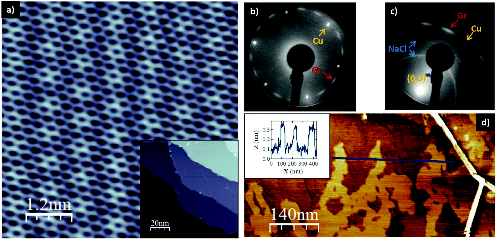 | ||
| Fig. 1 (a) STM image of 1ML of Gr/Cu(111) showing a moiré pattern (0.375 nA, 827.4 mV, (5.9 × 5.9) nm2). Inset: Zoom out of the STM image (100.2 × 100.2) nm2 (0.099 nA, 826.5 mV). (b) LEED pattern of a ML of Gr/Cu(111) at 135 eV. The modulated ring corresponds to Gr while the spots stem from Cu(111). (c) LEED pattern of NaCl/Gr/Cu(111) at 59 eV. The two inner rings belong to the NaCl film, while the outer one belongs to the Gr monolayer and the spots belong to Cu(111). For a better visualization, the (0,0) Cu spot is off-center. (d) AFM image (700.7 × 349.3) nm2 of a Gr/Cu(111) sample partially covered with NaCl. On the right-hand side a wrinkle (typical feature of Gr on metals) is visible. The inset shows the height profile along the blue line. | ||
After in situ characterization, the sample was taken out from UHV and characterized ex situ with AFM. An AFM image of submonolayer NaCl coverage is shown in Fig. 1d. A wrinkle, visible at the right side of the image, is a characteristic signature of a ML Gr12 which usually appears during the growth process on metal surfaces. The bright finger-like islands correspond to the NaCl film. In this case, the film growth was stopped in the submonolayer range in order to determine the thickness of the NaCl film. A profile in the image of Fig. 1d (inset) shows the height of the NaCl film with respect to the graphene of around 2.5 Å. This height is assigned to the thickness of a NaCl bilayer, 2.9 Å (ref. 15), within the typical error of the AFM.
It has been demonstrated that the moiré patterns in graphene can modify the adsorption properties.16 However, NaCl films are not affected by graphene corrugation due to the low interaction between the two surfaces. In order to prove it, we have grown Gr on a different metal substrate, Ir(111), with different moiré patterns. Fig. 2a shows a STM image of one of the characteristic moiré patterns of 1ML Gr/Ir(111). In the inset, the STM image shows the complete coverage of the Ir surface. The microspot LEED pattern (see Fig. 2b) shows the Ir (111) and the Gr spots as well as the typical pattern from the moiré of Gr/Ir(111), consisting of hexagons around the Ir integer spots. When NaCl is deposited at RT, two inner rings appear in the LEED (Fig. 2c). The structure is thus the same as that previously found for the Cu(111) surface, evidencing the weak NaCl–Gr interaction.
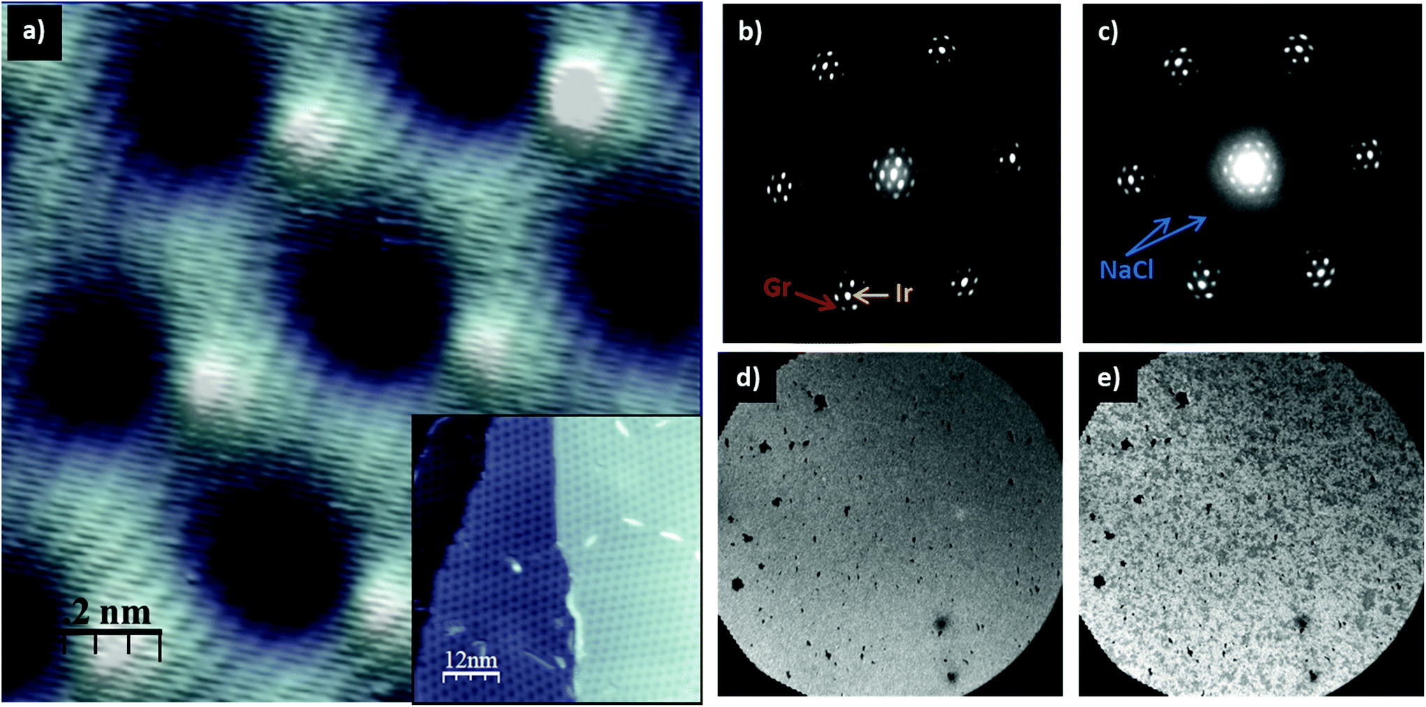 | ||
| Fig. 2 (a) STM image of 1ML of Gr/Ir(111) showing a typical moiré (13 × 13) nm2, (1.4 nA, 300 mV). Inset: Zoom out of the STM image. (b) Microspot LEED of 1ML of Gr/Ir(111) taken at 58 eV. (c) Microspot LEED of NaCl/Gr/Ir(111) taken at 58 eV. The two inner rings belong to NaCl. (d) and (e) LEEM images, FOV 20 μm and electron energy 18 eV, of NaCl/Gr/Ir(111) acquired just after salt evaporation (d) and a few seconds after (e). Electrons damage the NaCl film and as a result, a change in the contrast is visible in (e). | ||
Fig. 2d and e show two LEEM images with a field of view (FOV) of 20 μm, recorded in situ right after NaCl deposition and a few seconds later, respectively. In Fig. 2d the contrast is quite homogeneous because the surface, at this length scale, is fully covered by an ultra-thin film of salt. These LEEM images, together with ex situ AFM images (not shown), show a continuous layer of NaCl without pits or cracks and low surface roughness, supporting its use as a protective layer. Nonetheless, after a few seconds under electron beam irradiation the morphology of the surface changes. This damage can be readily seen as a change in the contrast of the LEEM image (Fig. 2e) where about 50% of the salt has already been desorbed. At this point it is worth mentioning that NaCl may experience photo-dissociation on Gr, leading to Na intercalation, as reported recently.17
A further important condition that capping layers have to fulfil is that they should not intercalate underneath the surface they are protecting. In this respect, it is still unclear whether NaCl intercalates through or adsorbs on graphene under ambient conditions. To shed some light on this open question we have characterized the samples with LEIS, a technique suited for this purpose due to its exceptional surface sensitivity as most of the signals come from the outermost atomic layer of the system under study.18 LEIS identifies elements by their masses; therefore the assignation of the main peaks based on their backscattering energies can be obtained following a simple equation derived from classical physics.18Fig. 3a shows the LEIS spectra for: a clean Cu(111) sample (ochre spectrum), a Gr/Cu sample (grey spectrum) and a NaCl/Gr/Cu sample (blue spectrum). For the clean Cu(111) sample, only the copper peak is visible, which manifests the absence of contaminants. After the growth of a Gr ML, there are no peaks at all. The copper peak was not expected since the sample is completely covered by graphene and LEIS is only sensitive to the last atomic layer. One might expect the presence of carbon emission which should be visible as any other element with this technique. However, for graphitic carbon or graphene an unusual strong matrix effect has been observed,19 which explains the absence of its signal in the spectrum. This phenomenon is related with the electronic structure of graphene that causes a strong neutralization of the backscattered helium ions.19 Hence, no peaks are observed. Finally, the LEIS spectrum of the NaCl/Gr/Cu sample displays two peaks that can be assigned to Na and Cl. Fig. 3b compares the LEIS spectra of a NaCl/Cu sample (upper green spectrum) with those of a NaCl/G/Cu sample (lower blue spectrum). Both NaCl evaporations have been performed under the same experimental conditions (evaporation time and substrate temperature). Nonetheless for the metal substrate the Na signal intensity is lower compared to that of graphene. Besides, a Cu peak appears in the upper spectrum, indicating that NaCl has not completely covered the whole metal surface. In contrast and as also demonstrated by the LEEM image shown in Fig. 2d, a continuous NaCl film covers the whole graphene surface, proving that the wetting of graphene takes place faster than that of the metal substrates. This set of consecutive experiments, where the different layers have been grown to build up the whole system step by step, evinces that NaCl remains on the surface and does not intercalate through graphene under ambient conditions. Although in the LEIS technique the intensity of a peak cannot be easily quantified, the fact that the Na signal is much higher than that of Cl suggests a higher neutralization probability of the He ions impeaching on negative Cl atoms. Other structural reasons such as buckling or surface relaxation in the salt layer cannot be excluded.
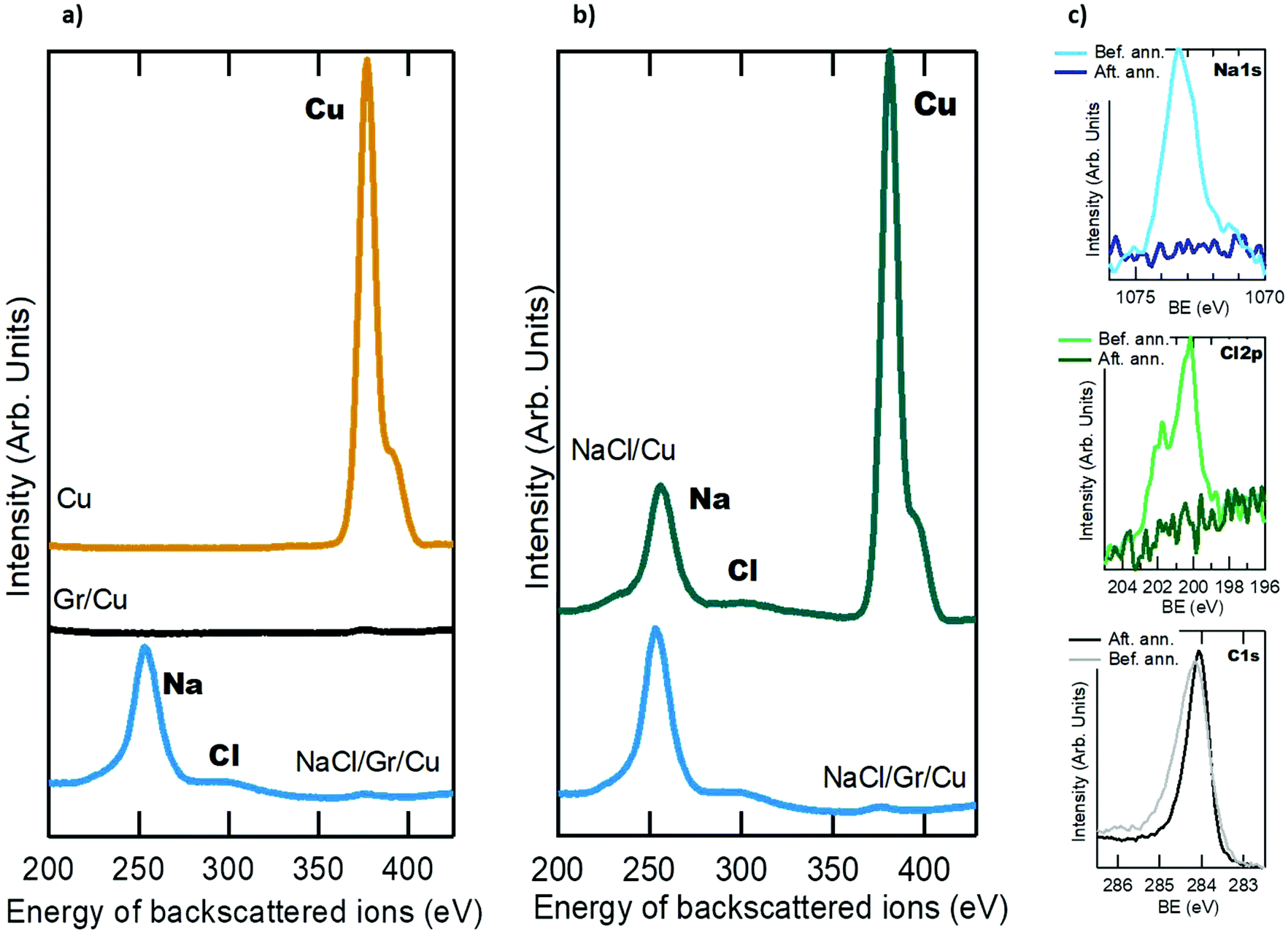 | ||
| Fig. 3 (a) LEIS spectra obtained at 0.5 keV, 10 mA, 2 × 10⁻⁷ mbar of He of clean Cu(111) (ochre), Gr/Cu(111) (grey), NaCl/Gr/Cu (blue) samples, respectively. (b) LEIS spectra obtained at 0.5 keV, 10 mA, 2 × 10⁻⁷ mbar of He of NaCl/Cu (green) and NaCl/Gr/Cu (blue) samples. (c) Upper, medium and lower panels: Na 1s, Cl 2p and C 1s core levels, respectively, of a NaCl/Gr/Ir(111) sample after several days under ambient conditions, before and after annealing at 823 K under UHV. | ||
Finally, we have evaluated by XPS the chemical interaction at the NaCl/Gr interface and the stability of the ultra-thin NaCl film under ambient conditions as well as its protective capacity in a non-vacuum environment. Fig. 3c (upper, middle and lower panels) shows the Na 1s, Cl 2p and C 1s core levels, respectively, of a sample after several days in air (closed room, at RT and 30% of humidity), before and after an annealing treatment under UHV at about 823 K. As can be seen, prior to the annealing, NaCl remains on the surface, showing its stability under ambient conditions. The measured binding energies of Na 1s and Cl 2p peaks are 1073.3 and 200.1 eV, respectively. Both peaks are shifted 2 eV towards higher binding energies as compared to a freshly cleaved NaCl single crystal.20 This shift can be ascribed to the –O and –OH groups adsorbed on top of the salt surface, implying that the NaCl film behaves as a sponge, capturing oxygen related contaminants and therefore preventing the ageing of graphene by these very same groups. The lower panel of Fig. 3c shows the C 1s core level of the same sample after several days in air. Before the annealing treatment, the peak slightly widens with a tail at higher binding energies associated with the adsorbed species on top of graphene (mainly NaCl). The main component at 284.1 eV can be assigned to C-sp2.21,22 To remove the protective layer an annealing treatment under UHV at about 823 K was carried out, until Na 1s and Cl 2p signals completely disappear (see the XPS spectra in Fig. 3c, upper and middle panels). After the annealing, the high binding energy tail of the C 1s peak completely vanished, together with the Na and Cl signals, and only the sp2 graphene component remains (Fig. 3d, lower panel). Even though before annealing, the C 1s component has a tail that suggests some sort of interaction between both interfaces, we would like to stress that after a mild annealing the tail completely disappears and the sp2 component remains unaltered. This slight modification of the C 1s lineshape and the recovery after annealing indicate that the chemical interaction of the salt and graphene is very weak. Moreover, in a recent work we were able to characterize the electronic band of the NaCl/Gr system, demonstrating that there is no modification of the graphene band structure at the Dirac-cone bands.17 Although from the structural point of view the lattice parameter of the NaCl compresses about 10% in the very first layers (see the LEED patterns in Fig. 1c and 2c, and ref. 15 and 23), this modification remains on the NaCl film without affecting graphene, as has been reported even for more interacting systems.24
In summary, it can be confirmed that NaCl does not chemically interact with Gr. In addition, upon annealing the sample, which removes the protective layer, the graphene surface displays the same structural perfection of an untreated graphene without showing any structural or chemical damage.
3. Conclusions
We have carried out a thorough characterization of the NaCl/Gr interface, proving that ultra-thin NaCl films fully cover the graphene surface, protecting it from oxidation while presenting negligible interaction with the underlying graphene. Structural characterization performed by the combination of STM, LEEM and AFM shows that NaCl grows as a bilayer which completely covers the graphene surface. LEED shows that NaCl films present a multi-domain structure due to the low interaction between the Gr and NaCl surfaces whereas photoemission results corroborate the stability of the NaCl film after several days under ambient conditions as well as its negligible chemical interaction with graphene. Moreover, XPS also demonstrates that after removing the ultra-thin NaCl film, graphene remains undamaged. Finally, LEIS studies confirm that NaCl does not intercalate through graphene under ambient conditions. Taking all these results into account, we can conclude that NaCl ultra-thin films can be considered as a technologically relevant option to be used as protective layers to prevent the ageing of graphene.4. Experimental section
The growth and in situ characterization of the samples have been carried out in ultra-high vacuum (UHV) chambers, with a base pressure of 1 × 10⁻¹⁰ mbar. Ir(111) surfaces were cleaned by repeated cycles of argon ion sputtering and annealing under an oxygen atmosphere (T = 1373 K and Poxygen = 2 × 10⁻⁸ mbar). In order to avoid any residual oxygen on the surface, the last cleaning cycle was carried out without oxygen. Cu(111) samples were cleaned with cycles of sputtering and annealing (873 K). Graphene on Cu(111) was grown by thermal decomposition of C60 (Sigma Aldrich, 98% purity). These fullerenes were evaporated directly in the UHV system from a home-made evaporator based on a tantalum crucible and a type-K thermocouple spot-welded to it. The samples were kept at 1173 K during the evaporation.25 Graphene on Ir(111) was grown by the decomposition of ethene following the procedure described elsewhere.26 NaCl (99.999% Sigma Aldrich) was sublimated from a home-made Ta crucible annealed at 803 K controlled by a type-K thermocouple spot-welded to it, keeping the sample at RT. Structural in situ characterization has been carried out with an Omicron RT-STM and an Omicron LEED. WSxM software was used for data acquisition and analysis.27 XPS was used to characterize the chemical composition of the samples. XPS spectra were acquired in an ultrahigh vacuum (UHV) chamber with a base pressure of 1 × 10⁻⁹ mbar using a hemispherical electron energy analyser (SPECS Phoibos 150 spectrometer) and a monochromatic AlKα X-ray source (1489.74 eV). XPS spectra were recorded at the normal emission take-off angle, using an energy step of 0.05 eV and a pass-energy of 10 eV for high resolution data, which provides an overall instrumental peak broadening of 0.4 eV. LEIS was performed using the hemispherical analyser SPECS Phoibos 100 MCD-5, with the analyser operating in the CRR mode. He+ ions (0.5 keV) have been used as incoming ions. LEEM and microspot LEED were performed at the LEEM-PEEM experimental station of the CIRCE beamline of the ALBA Synchrotron.28 AFM characterization was done with Agilent 5500 PicoPlus equipment operating in the dynamic mode under ambient conditions. Silicon cantilevers (from AppNano) with a nominal radius smaller than 10 nm were employed. The images formed were of 1024 × 1024 pixels.Conflicts of interest
The authors declare no competing financial interest.Acknowledgements
This work has been supported by the EU Graphene Flagship funding (Grant Graphene Core2 785219), the Spanish MINECO (MAT2017-85089-C2-1R, MAT2016-80394-R, RTI2018-095303-B-C53 and RYC-2015-17730), the EU via the ERC-Synergy Program (Grant ERC-2013-SYG-610256 NANOCOSMOS) and the European Structural Funds via FotoArt-CM project (S2018/NMT-4367).References
- K. S. Novoselov, A. K. Geim, S. V. Morozov, D. Jiang, Y. Zhang, S. V. Dubonos, I. V. Grigorieva and A. A. Firsov, Electric Field Effect in Atomically Thin Carbon Films, Science, 2004, 306(5696), 666–669 CrossRef CAS.
- K. S. Novoselov, V. I. Fal'ko, L. Colombo, P. R. Gellert, M. G. Schwab and K. Kim, A roadmap for graphene, Nature, 2012, 490, 192 CrossRef CAS.
- Y. Shi, Y. Ji, F. Hui, H. H. Wu and M. Lanza, Ageing mechanisms and reliability of graphene-based electrodes, Nano Res., 2014, 7(12), 1820–1831 CrossRef CAS.
- A. S. Mayorov, R. V. Gorbachev, S. V. Morozov, L. Britnell, R. Jalil, L. A. Ponomarenko, P. Blake, K. S. Novoselov, K. Watanabe, T. Taniguchi and A. K. Geim, Micrometer-Scale Ballistic Transport in Encapsulated Graphene at Room Temperature, Nano Lett., 2011, 11(6), 2396–2399 CrossRef CAS.
- A. K. Geim and I. V. Grigorieva, van der Waals heterostructures, Nature, 2013, 499(7459), 419–425 CrossRef CAS PubMed.
- A. Sundararajan, M. J. Boland, D. Patrick Hunley and D. R. Strachan, Doping and hysteretic switching of polymer-encapsulated graphene field effect devices, Appl. Phys. Lett., 2013, 103(25), 253505 CrossRef.
- G. Skoblin, J. Sun and A. Yurgens, Encapsulation of graphene in Parylene, Appl. Phys. Lett., 2017, 110(5), 3–7 CrossRef.
- J. G. Roberts, S. Ho, M. A. Van Hove and G. A. Somorjai, Tensor low-energy electron diffraction analysis of the surface structure of NaCl (100) thin films grown on Pd (100) and Pt (111), Surf. Sci., 1999, 437, 75–85 CrossRef CAS.
- S. Folsch, U. Barjenbruch and M. Henzler, Atomically thin epitaxial films of NaCl on germanium, Thin Solid Films, 1989, 172, 123–132 CrossRef.
- R. Bennewitz, A. Foster, L. Kantorovich, M. Bammerlin, C. Loppacher, S. Schar, M. Guggisberg, E. Meyer and A. Shluger, Atomically resolved edges and kinks of NaCl islands on Cu(111): Experiment and theory, Phys. Rev. B: Condens. Matter Mater. Phys., 2000, 62(3), 2074–2084 CrossRef CAS.
- G. Shi, L. Chen, Y. Yang, D. Li, Z. Qian, S. Liang and L. Yan, Two-dimensional Na – Cl crystals of unconventional stoichiometries on graphene surface from dilute solution at ambient conditions, Nat. Chem., 2018, 2–5 Search PubMed.
- I. Palacio, G. Otero-irurueta, C. Alonso, J. I. Martínez, E. López-, I. Muñoz-ochando, H. J. Salavagione, M. F. López, M. García-, J. Méndez, G. J. Ellis and J. A. Martín-gago, Chemistry below graphene : decoupling epitaxial graphene from metals by potential-controlled electrochemical oxidation, Carbon, 2018, 129, 837–846 CrossRef CAS.
- P. Merino, M. Svec, A. L. Pinardi, G. Otero and J. A. Martin-Gago, Strain-Driven Moire Superstructures of Epitaxial Graphene on Transition Metal Surfaces, ACS Nano, 2011, 5(7), 5627–5634 CrossRef CAS PubMed.
- R. Bennewitz, V. Barwich, M. Bammerlin, C. Loppacher, M. Guggisberg, A. Baratoff, E. Meyer and H. Güntherodt, Ultrathin films of NaCl on Cu (111): a LEED and dynamic force microscopy study, Surf. Sci., 1999, 438(1), 289–296 CrossRef CAS.
- K. Lauwaet, K. Schouteden, E. Janssens, C. Van Haesendonck and P. Lievens, Dependence of the NaCl/Au(111) interface state on the thickness of the NaCl layer, J. Phys.: Condens. Matter, 2012, 24(47), 475507 CrossRef.
- M. Petrović, P. Lazić, S. Runte, T. Michely, C. Busse and M. Kralj, Moiré-regulated self-assembly of cesium adatoms on epitaxial graphene, Phys. Rev. B, 2017, 96(8), 085428 CrossRef.
- I. Palacio, L. Aballe, M. Foerster, D. G. de Oteyza, M. García-Hernández and J. A. Martín-Gago, Reversible graphene decoupling by NaCl photo-dissociation, 2D Mater., 2019, 6(2), 025021 CrossRef.
- C. V. Cushman, P. Brüner, J. Zakel, G. I. Major, B. M. Lunt, T. Grehl, N. J. Smith and M. Linford, Low Energy Ion Scattering (LEIS). A Practical Introduction to its Theory, Instrumentation, and Applications, Anal. Methods, 2016, 3419–3439 RSC.
- S. Průsa, P. Procházka, P. Bábor, T. Šikola, R. Ter Veen, M. Fartmann, T. Grehl, P. Brüner, D. Roth, P. Bauer and H. H. Brongersma, Highly Sensitive Detection of Surface and Intercalated Impurities in Graphene by LEIS, Langmuir, 2015, 31(35), 9628–9635 CrossRef.
- B. C. Beard, Fresh Cleaved Single Crystal NaCl, XPS Spectra, Al Source, Surf. Sci. Spectra, 1993, 2(2), 91 CrossRef CAS.
- A. B. Preobrajenski, M. L. Ng, A. S. Vinogradov and N. Mårtensson, Controlling graphene corrugation on lattice-mismatched substrates, Phys. Rev. B: Condens. Matter Mater. Phys., 2008, 78(7), 2–5 CrossRef.
- R. Larciprete, S. Fabris, T. Sun, P. Lacovig, A. Baraldi and S. Lizzit, Dual path mechanism in the thermal reduction of graphene oxide, J. Am. Chem. Soc., 2011, 133(43), 17315–17321 CrossRef CAS.
- J. Repp, G. Meyer and K.-H. Rieder, Snell's law for surface electrons: refraction of an electron gas imaged in real space, Phys. Rev. Lett., 2004, 92(3), 036803 CrossRef.
- P. Merino, L. Rodrigo, A. L. Pinardi, J. Méndez, M. F. López, P. Pou, R. Pérez and J. A. Martín Gago, Sublattice Localized Electronic States in Atomically Resolved Graphene-Pt(111) Edge-Boundaries, ACS Nano, 2014, 8(4), 3590–3596 CrossRef CAS.
- J. Azpeitia, G. Otero-Irurueta, I. Palacio, J. I. Martinez, N. Ruiz del Árbol, G. Santoro, A. Gutiérrez, L. Aballe, M. Foerster, M. Kalbac, V. Vales, F. J. Mompeán, M. García-Hernández, J. A. Martín-Gago, C. Munuera and M. F. López, High-quality PVD graphene growth by fullerene decomposition on Cu foils, Carbon, 2017, 119, 535–543 CrossRef CAS PubMed.
- J. Coraux, A. T. N'Diaye, M. Engler, C. Busse, D. Wall, N. Buckanie, F.-J. Meyer zu Heringdorf, R. van Gastel, B. Poelsema and T. Michely, Growth of graphene on Ir(111), New J. Phys., 2009, 11(2), 023006 CrossRef.
- I. Horcas, R. Fernández, J. M. Gómez-Rodríguez, J. Colchero, J. Gómez-Herrero and A. M. Baro, WSXM: A software for scanning probe microscopy and a tool for nanotechnology, Rev. Sci. Instrum., 2007, 78(1), 013705 CrossRef CAS.
- L. Aballe, M. Foerster, E. Pellegrin, J. Nicolas and S. Ferrer, The ALBA spectroscopic LEEM-PEEM experimental station: Layout and performance, J. Synchrotron Radiat., 2015, 22, 745–752 CrossRef CAS.
Footnotes |
| † Present address: IMDEA Nanociencia. Ciudad universitaria de Cantoblanco 28049, Madrid, Spain. |
| ‡ Present address: Regional Centre of Advanced Technologies and Materials, Department of Physical Chemistry, Faculty of Science, Palacký University, Šlechtitelů 27, 78371 Olomouc, Czech Republic. |
| This journal is © The Royal Society of Chemistry 2019 |