
Investigating the detection limit of subsurface holes under graphite with atomic force acoustic microscopy†
Kevin
Yip
 ,
Teng
Cui
,
Yu
Sun
and
Tobin
Filleter
*
,
Teng
Cui
,
Yu
Sun
and
Tobin
Filleter
*
Department of Mechanical and Industrial Engineering, University of Toronto, Toronto, ON M5S 3G8, Canada. E-mail: filleter@mie.utoronto.ca
First published on 22nd May 2019
Abstract
The subsurface imaging capabilities of atomic force acoustic microscopy (AFAM) was investigated by imaging graphite flakes suspended over holes in a silicon dioxide substrate. The graphite thickness and the hole size were varied to determine the detection limit on the maximum graphite thickness and the smallest detectable hole size. Parameters including operating frequency, eigenmode, contact force, and cantilever stiffness were investigated for their influence of defect detection. AFAM was reliably able to detect 2.5 μm diameter holes through a maximum graphite thickness of 570 nm and sub 100 nm holes through 140 nm of graphite. The smallest detectable defect size was a 50 nm hole covered by an 80 nm thick graphite flake. Increasing the graphite thickness and decreasing the hole size both resulted in a decrease in subsurface contrast. However, the non-linear trend observed from increasing the graphite thickness indicates thickness has a greater effect on subsurface defect detection than variations in defect size. Through investigating various parameters, we have found certain cases to increase the observed contrast of the embedded subsurface holes, however the smallest detectable defect size remained the same. This technique's ability to reveal sub 100 nm defects buried under graphite has previously only been demonstrated in much softer polymer systems.
1. Introduction
With the increasing applicability of nanostructured materials in micro/nano electronics, there exists a need for a non-destructive testing (NDT) technique capable of subsurface defect detection with nanoscale resolution.1 Traditional ultrasonic based detection systems such as ultrasonic testing for detecting cracks in pipelines are not applicable on the micro/nanoscale due to diffraction effects as the wavelength of ultrasound is much greater than the thickness of these systems let alone the defects.2 Common imaging techniques such as scanning electron microscopy (SEM) and transmission electron microscopy (TEM) can cause irradiation damage to the sample.3 Additionally, the samples require sectioning to provide any substantial subsurface information which is destructive. A technique known as scanning acoustic microscopy (SAM) is capable of subsurface characterization but is also limited by diffraction, having a defect resolution of hundreds of microns at a depth of a few mm.4The atomic force microscope (AFM) is a tool commonly used for surface characterization that allows for nanoscale imaging with minimal sample damage. Combining the high spatial resolution of the AFM with the use of ultrasound allows for non-destructive subsurface defect detection. There are many different variations of subsurface AFM imaging which can be categorized as ultrasonic force microscopy (UFM),5–8 atomic force acoustic microscopy (AFAM),9–14 and heterodyne force microscopy (HFM).15–18 The main differences between these techniques are the drive frequencies and how the ultrasound is applied, from below the sample, probe, or both. These techniques have been shown to image subsurface defects at various depths with different materials, from soft polymers like polystyrene (PS) and poly(methyl methacylate) (PMMA) to stiffer materials such as silicon. When determining the maximum thickness at which the subsurface defect can still be detected, a soft polymer matrix with embedded nanoparticles offers the highest depth detection of approximately one micron,19 although a surprising depth of seven microns has been reported.20 The subsurface detection capabilities of AFAM have also been investigated on a stiffer material such as silicon, where various geometries of buried voids were imaged in the silicon.11 These structures exhibited a decrease in subsurface contrast as they were buried deeper in the silicon, it was noted that the lateral sizes of these buried voids were on the scale of microns.
Graphite is a popular additive for lubricants and has become an attractive material system for subsurface AFM imaging as its inherent defects provide strong subsurface contrast.21–23 Unlike the low out-of-plane modulus of PMMA and PS (7.7 and 5.6 GPa respectively),24 the higher out-of-plane modulus of graphite (36.5 GPa)25 makes it an ideal system for investigating the subsurface AFM techniques as graphite flakes can act as a suspended membrane over a patterned substrate. Using this system, Dinelli et al. demonstrated UFM's subsurface capability by revealing trench structures with a height of 250 nm and a width of one micron that were supporting a 50 nm thick graphite flake.8 A recent study conducted by Zhang et al. showed that imaging in a liquid environment with higher harmonic AFM can reveal buried holes from 2 μm to 200 nm in diameter, beneath 50 nm of graphite.26 While both these studies have demonstrated the capability of subsurface imaging, a comprehensive study of the limits of either technique has not been conducted. Herein, using pre-fabricated microcavities covered by graphite, we investigated the subsurface defect detection capabilities of AFAM by varying both the graphite thickness as well as the defect sizes from microns to sub 100 nm's. In addition, imaging parameters such as operating frequency, higher cantilever eigenmodes, contact force, and cantilever stiffness were investigated to provide more quantitative insight into the technique.
2. Materials & methods
Arrays of holes with varied diameters were fabricated on a SiO2/Si substrate using electron beam lithography followed by reactive ion etching. Two substrates were developed, one consists of holes with a diameter of 2.5 μm and the other substrate consists of holes with decreasing diameter from 2.5 μm to 20 nm. Their respective SEM images are shown in Fig. 1a and b. The SEM image of the smallest hole confirms the 20 nm diameter. AFM topography linescans in Fig. 1c reveal the etch depths for the different substrates. The substrate with consistent hole sizes had an etch depth of 400 nm while the substrate with varied diameters show a decrease in etch depth from 290 nm for the 2.5 μm holes to 9 nm for the 50 nm holes. AFM topographic imaging had difficulty accurately resolving sub 100 nm holes due to blunting of the tip. This decrease in etch depth for the smaller diameter holes is due to the reactive ion etch procedure, as the ions are unable to etch as deeply due to the small hole size. Various thicknesses of graphite flakes were deposited onto the patterned silicon substrates via mechanical exfoliation of highly oriented pyrolytic graphite (HOPG). Thicknesses ranging from one micron down to 30 nm were obtained from this technique. This sample configuration allows us to emulate subsurface defects with exact size and location. All experiments were performed on an Asylum MFP 3D AFM in ambient air (12% relatively humidity) using silicon cantilevers with normal spring constants from 1.13 N m−1 to 21.8 N m−1. Additionally, all topography line scans of the various graphite flakes shown throughout can be found in the ESI (Fig. S1) in section S1.†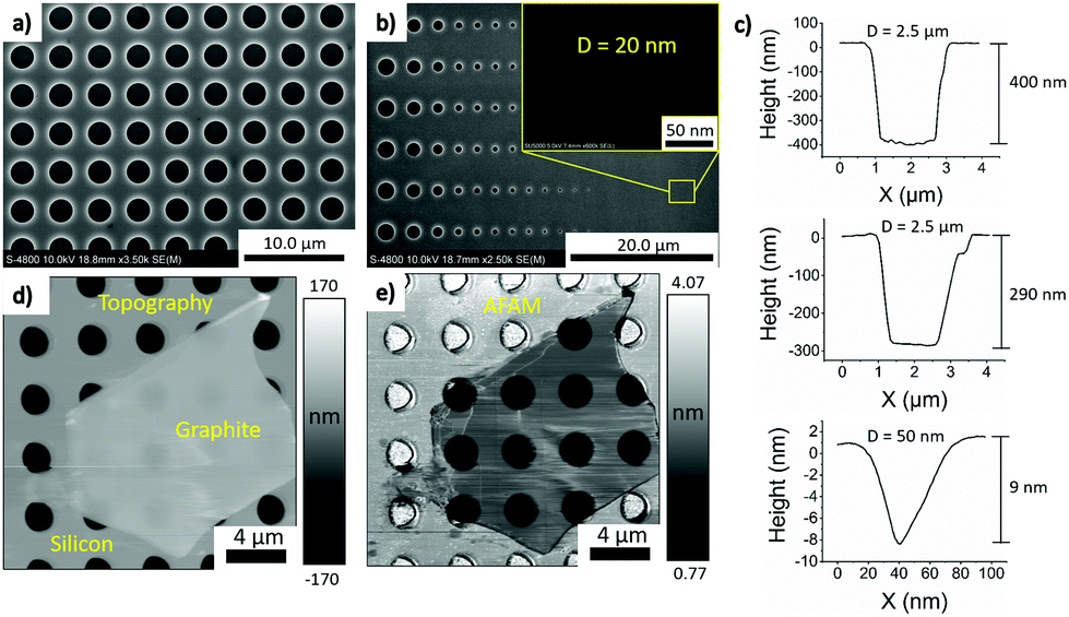 | ||
| Fig. 1 SEM images of the two pre-patterned silicon substrates with (a) 2.5 μm holes, and (b) decreasing hole sizes from 2.5 μm to 20 nm shown in upper inset, (c) AFM height line scan of 2.5 μm holes at two different etch depths and a 50 nm hole. (d) AFM topographic image of a 30 nm graphite flake and its corresponding, (e) AFAM amplitude image revealing subsurface holes at 350 kHz and 110 nN. The cantilever used had a stiffness of 1.8 N m−1 (PPP-RT-FMR). | ||
The AFAM setup27 uses a custom-built piezo-stack which the sample is mounted onto using phenyl salicylate,21 more information of the setup used can be found in section S2 of the ESI.† As ultrasound propagates through the sample from the piezo, the tip scans across the surface recording changes in the topography, amplitude, and phase simultaneously.27 The amplitude image is primarily used for subsurface AFAM imaging as it directly represents the cantilever oscillation at the given drive frequency. The piezo drive voltage was consistently 1 V, while the frequency was chosen to be 10–30 kHz higher than the contact resonance frequency, which was determined by sweeping the frequency while the tip is in contact with the surface. The contact force was chosen to be low enough to ensure that no sample damage would take place. The operating parameters used for graphite flakes on the substrate consisting of only 2.5 μm holes was 350 kHz at 110 nN, and 325 kHz at 55 nN on the substrate with varying hole sizes given that the contact resonance frequency was 320 kHz. A typical AFM topographic image of a suspended 30 nm graphite flake over 2.5 μm holes is shown in Fig. 1d with its corresponding AFAM amplitude image in Fig. 1e. The buried holes beneath the graphite flake are barely visible in the topographic image but are clearly defined in the AFAM image.
3. Results & discussion
3.1. Effect of graphite thickness on the detection of 2.5 μm holes
A systematic approach was taken to determine the detection limits of AFAM, beginning with a thin 30 nm graphite flake and then gradually increasing the flake thickness until no subsurface contrast was visible. Fig. 2a shows a graphite flake with a thickness ranging from 463–135 nm and its corresponding SEM, AFM topography and AFAM amplitude images. The graph illustrated in Fig. 2b reveals the amplitude change (contrast) over a variety of graphite thicknesses. The amplitude change is defined as the observed amplitude measured on the graphite flake suspended over the hole subtracted from the background amplitude measured on graphite flake deposited on the silicon dioxide substrate (see Fig. S2 in section S3 of the ESI†). This technique can clearly resolve the buried holes under 570 nm of graphite, as shown in the upper inset of Fig. 2b. However, holes beneath a 900 nm thick graphite flake are undetectable and beyond the thickness detection limit of AFAM (lower right inset of Fig. 2b).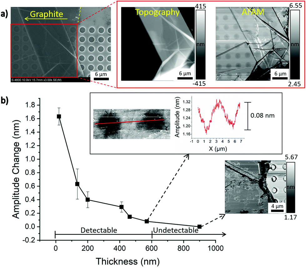 | ||
| Fig. 2 (a) SEM image of graphite flake ranging in thickness from 463–135 nm (left). Topographic AFM image (middle). AFAM amplitude image at 350 kHz, 110 nN (right). (b) Graph depicting amplitude contrast at 350 kHz, 110 nN for graphite thicknesses from 900–30 nm. Upper inset shows holes corresponding to 570 nm thick graphite, the maximum thickness that contrast can be obtained. Lower right inset showing no contrast of holes beneath 900 nm of graphite. The cantilever used had a stiffness of 1.8 N m−1 (PPP-RT-FMR). | ||
The SEM image shown in Fig. 2a reinforces the need for a NDT technique capable of nanoscale resolution as only the thinnest regions of graphite (170 nm) show contrast of the subsurface holes. The AFM topographic image in Fig. 2a shows no indication of the buried 2.5 μm holes. For the given parameters, the thickness detection limit for detecting buried 2.5 μm holes is 570 nm of graphite. The true thickness limit is likely slightly higher than 570 nm of graphite but less than 900 nm given that the holes are still detectable at a graphite thickness of 570 nm. With a constant hole size, an increase in graphite thickness results in a decreased amplitude change (contrast). The cantilever amplitude varies as the contact resonance frequency shifts due to changes in the mechanical properties (contact stiffness).27 Parlak and Degertekin showed that increasing the radius of an embedded cylindrical cavity causes a larger decrease in the local contact stiffness or contact resonance frequency.28 In our case, the subsurface holes act as embedded cavities which reduce the local contact stiffness, causing a reduction in tip amplitude. As the holes become increasingly buried by graphite, the reduction in local contact stiffness decreases until a point is reached where no change is observed, which occurs a little over 570 nm of graphite.
Rayleigh scattering is another possible contrast mechanism that has been investigated in a similar technique known as HFM. This mechanism is based on the scattering of high frequency acoustic waves due to the presence of nanoparticles or voids,17,18,29 which causes a reduction in the amplitude and most notably the phase. Verbiest et al. has shown in HFM that scattering of 3 MHz acoustic waves from the presence of a nanoparticle can cause amplitude and phase contrast above the particle, with the largest contrast coming from a difference in density.29 Given that the density difference in our case with a cavity in silicon is much lower than the reported Au in PMMA and a low drive frequency of 350 kHz, the amplitude contrast from Rayleigh scattering would be even lower. However, the addition of the graphite flake suspended over the hole may cause additional acoustic scattering contributing to some of the observed amplitude contrast. A reduction in contrast has also been observed for increases in defect depth for graphite26 and silicon.11
3.2. Effect of defect size on the detection limit of subsurface holes under graphite
To quantify the effects that a defect size scale reduction to the nanoscale has on AFAM, the other pre-patterned substrate with decreasing hole size was investigated with a similar experimental approach. To demonstrate AFAM's subsurface imaging capability for nanosized defects, an 80 nm thick graphite flake was deposited on the patterned substrate and imaged with the AFAM technique. Fig. 3a shows the AFM topography image of the large 80 nm graphite flake with no contrast of the buried holes. On the contrary, AFAM amplitude images revealed all hole sizes down to 50 nm (Fig. 3b–e). The apparent diameter of the 50 nm hole in Fig. 3e appears to be closer to 100 nm which is in contrast to results published in literature.15,19,20 One possible explanation for this is tip blunting from scanning in contact on a stiff material such as graphite, resulting in a much larger contact area and lower overall resolution. In the previously cited articles, they imaged nanoparticles in a soft polymer so their tip maintains their sharpness, resulting in the same apparent diameter. It should be noted that the 50 nm hole shown is off screen, further to the right of Fig. 3b.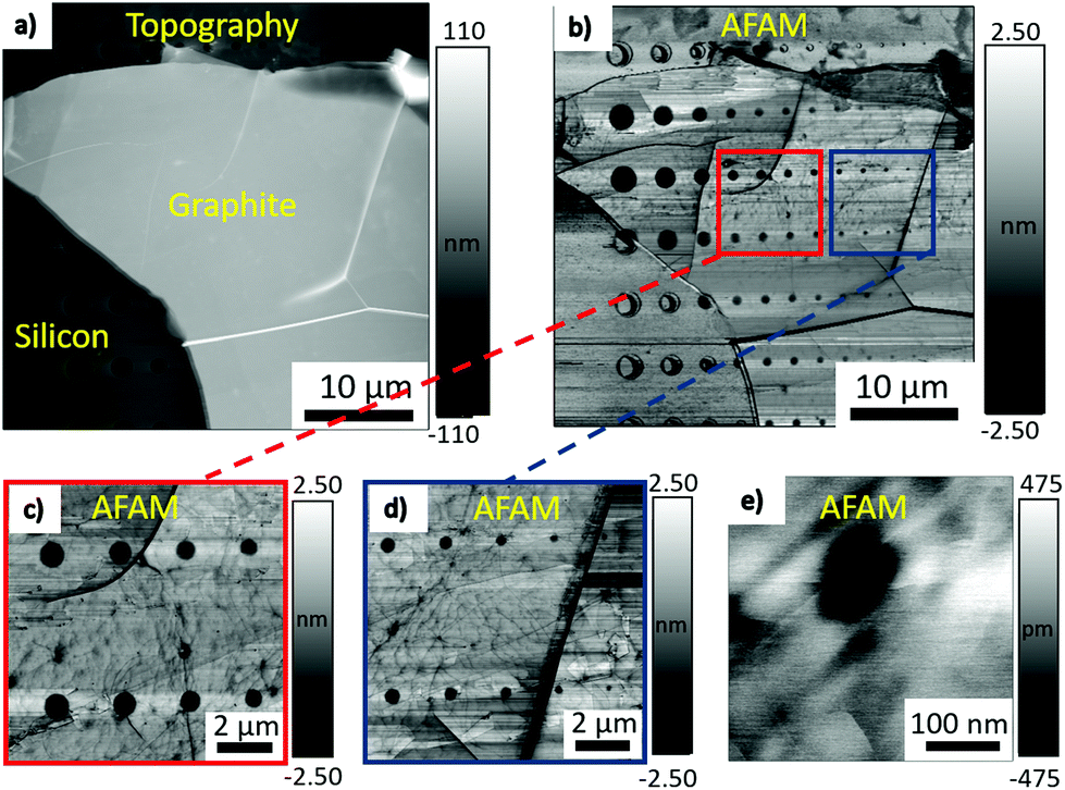 | ||
| Fig. 3 (a) AFM topography of 80 nm thick graphite flake. (b) AFAM amplitude image at 325 kHz, 55 nN. (c) Holes ranging from 1–0.7 μm. (d) Holes ranging from 600–200 nm. (e) 50 nm hole with an apparent diameter of 100 nm. The cantilever used had a stiffness of 1.8 N m−1 (PPP-RT-FMR). | ||
A quantitative comparison was performed on a 140 nm thick graphite flake suspended over decreasing hole sizes. SEM, AFM topography and AFAM amplitude images are shown in Fig. 4a. Similar to previous SEM images, the larger subsurface holes are visible through the graphite but nowhere close to the resolution of the AFAM amplitude images in resolving the much smaller holes. AFM topography shows no indication of the buried holes, and both SEM/AFAM images show the graphite flake is suspended over holes 500 nm and smaller. The graph in Fig. 4b illustrates a decreasing amplitude change with a decrease in the diameter of subsurface holes. This decreasing trend is similar to increasing the graphite thickness. The smallest detectable defect size was 80 nm for a graphite thickness of 140 nm (lower inset of Fig. 4b). A decreasing hole size results in less local contact stiffness change as well as less acoustic scattering resulting in a lower observed amplitude change. This technique shows that it is possible to resolve sub 100 nm defects in a stiff material system, which has only previously been shown for polymers.12,19 It is important to note that the sub 100 nm holes is extremely shallow as compared to their lateral dimension, approximately 9 nm. With AFAM, it is clear that the lateral dimension has a larger influence than the vertical height of the defect. As shown in the insets of Fig. 4b, AFAM's ability to reveal edges and steps in graphite compared to traditional AFM techniques can make it difficult to detect the nanoscale subsurface holes as they can dominate the signal.
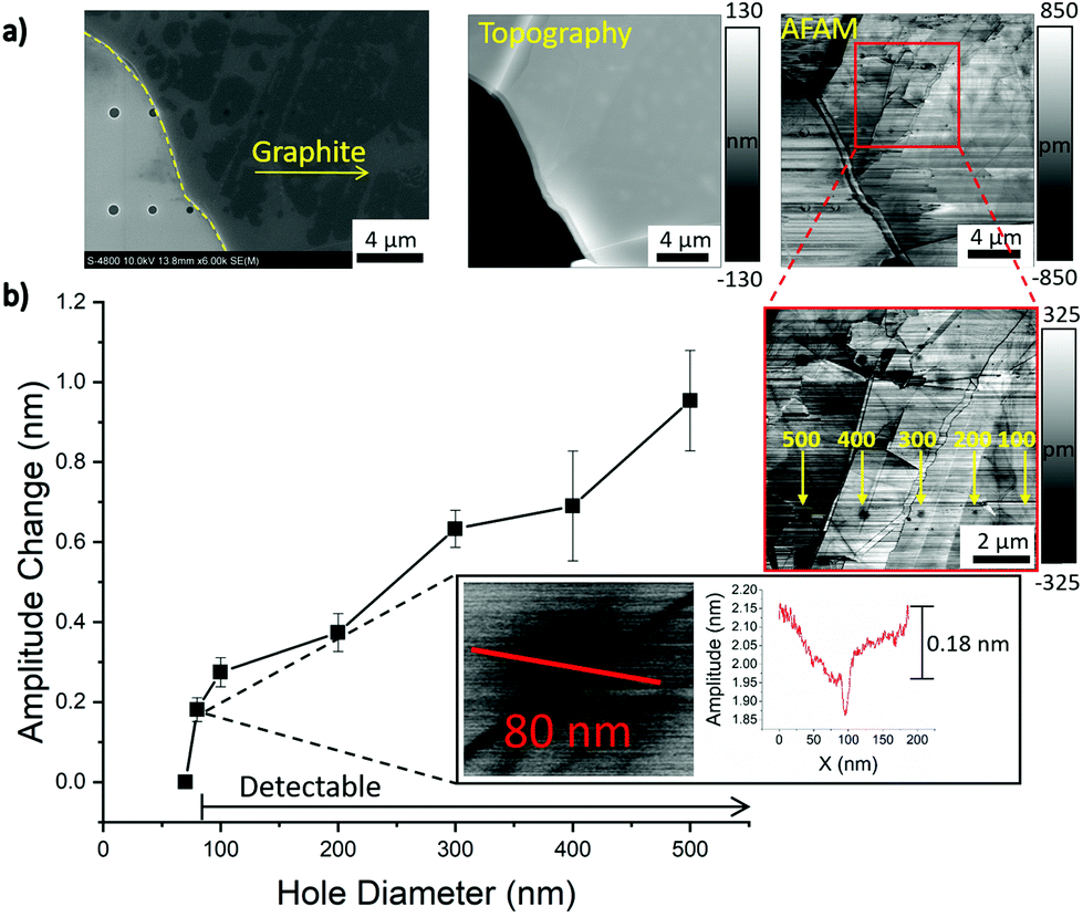 | ||
| Fig. 4 (a) SEM image of 140 nm graphite flake over holes of decreasing size (left), AFM topography (middle), AFAM amplitude image at 325 kHz, 55 nN (right). (b) Graph showing decrease in amplitude contrast with decreasing hole size. Upper inset showing AFAM amplitude image of holes ranging from 500–100 nm. Bottom inset showing AFAM amplitude image of 80 nm hole. The cantilever used had a stiffness of 1.8 N m−1 (PPP-RT-FMR). | ||
From Fig. 2 and 4, a non-linear trend is observed for increases in thickness while a linear trend for a decrease in defect size. Taking contact stiffness as the primary mechanism, FEA results from Killgore et al. show good agreement in that an increase in defect depth causes a non-linear decrease in contact stiffness contrast while a decrease in defect diameter results in a linear decrease in contact stiffness contrast.12 The non-linear decrease in contrast for increasing thickness was also observed in FEA simulations from Sharahi et al.17 For Rayleigh scattering, both cases of decreasing defect size17,29 and increasing thickness29 showed non-linear decreases in contrast. From Verbiest et al., the amplitude contrast in Rayleigh scattering is much more affected by defect radius than its distance from the surface given that the scattered wave intensity is proportional to the radius cubed.29 Knowing this, Rayleigh scattering likely has very little impact on the amplitude contrast seen in Fig. 4 as the defects are so small. The primary contrast mechanism is therefor attributed to variations in the contact stiffness.
To explain why the thickness has a greater effect than defect size on subsurface contrast, a model proposed by Castellanos-Gomez et al. for the deflection of suspended MoS2 nanosheets over holes indicates the stiffness scales with t3R−2, where t is the thickness and R is the radius of the hole the nanosheet is suspended over.30 While this model was proposed for thin 20 nm flakes, the first part of the equation with the thickness and radius excluding pretension was obtained from classical plate theory with a thin circular film subjected to a point load.31 This model indicates that the thickness has a larger effect on stiffness than radius, however there is some contradiction in that this model indicates a non-linear relationship between stiffness and radius while the FEA simulations,12 and our experimental results showed a linear relationship.
3.3. Effect of operating frequency and eigenmodes on subsurface defect detection
As mentioned earlier, drive frequency is one of the operating parameters that was investigated on its influence of subsurface defect detection. It is generally accepted that the drive frequency for AFAM imaging should be near the contact resonance frequency so that changes in the contact resonance frequency can be shown as amplitude contrast,10,11,19 but there is little information regarding the range of acceptable frequencies.32 While the cantilevers amplitude increases the closer it is to the contact resonance, it is unclear what effect this may have on its subsurface detection capabilities. Fig. 5 shows the influence of frequency on subsurface defect detection on a 160 nm thick graphite flake suspended over the silicon substrate with decreasing hole size. To better quantify the techniques ability to resolve defects, the signal-to-noise (S/N) ratio was plotted in addition to the amplitude change (contrast). The S/N ratio is defined as the magnitude of the amplitude signal in the hole divided by the standard deviation in the background graphite signal19 (see Fig. S2 in section S3 of the ESI†).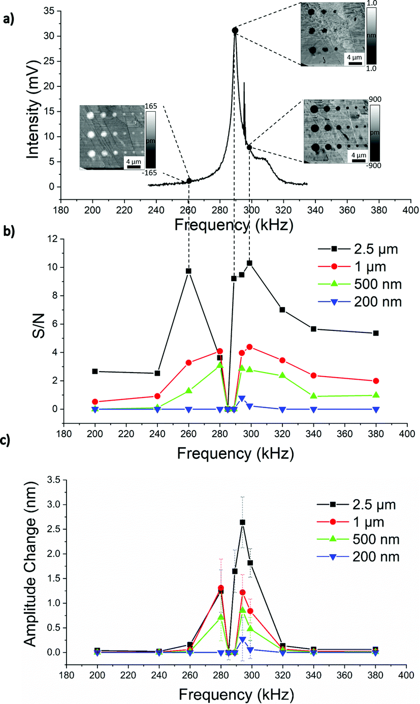 | ||
| Fig. 5 (a) First contact resonance peak centered at 289 kHz and the associated AFAM amplitude images at various frequencies at 110 nN. (b) S/N ratio of AFAM images taken at various frequencies and hole sizes. (c) Amplitude change of AFAM images taken at various frequencies and hole sizes. The cantilever used had a stiffness of 1.13 N m−1 (ASYELEC). | ||
Within ±5 kHz of the contact resonance frequency, the obtained AFAM amplitude images show very poor contrast and resolution of the subsurface defects, which can be seen in Fig. 5a. The S/N graph indicates that the most optimal imaging conditions are slightly offset from the contact resonance peak, with the maximum occurring at 299 kHz which is 10 kHz above the resonance frequency. The subsurface contrast for the 200 nm holes quickly disappear as the frequency is further increased, however it is interesting to see that contrast for the large holes is still observable at over 100 kHz away from the contact resonance frequency. Subsurface contrast is also observed operating below the contact resonance frequency, however the contrast is inverted10,33 and is slightly worse in detection capabilities for the smaller holes. The amplitude change graph (Fig. 5c) is similar except the maximum contrast occurs at 294 kHz. This frequency is closer to the contact resonance so the higher magnitudes observed in the contrast is unsurprising, however the noise in the background signal is also higher which is why the S/N is not as high as in the 299 kHz case. One potential explanation for this may be that the cantilever is more susceptible to thermal noise when its operated closer to its resonance frequency. As the frequency shifts further away from the contact resonance frequency, the noise is greatly reduced (Fig. 5c).
Various articles have shown that imaging at higher cantilever eigenmodes can significantly improve subsurface contrast12,14,19,26 by utilizing the increased effective stiffness that these higher modes possess.12 The following Fig. 6 shows the effect of utilizing the higher eigenmodes as a function of hole size. The operating frequencies were 10–20 kHz above the corresponding eigenmode frequencies at a contact force of 110 nN. Given the high drive frequency associated with the third eigenmode, a drive amplitude of 8 V was applied to obtain a reasonable signal.
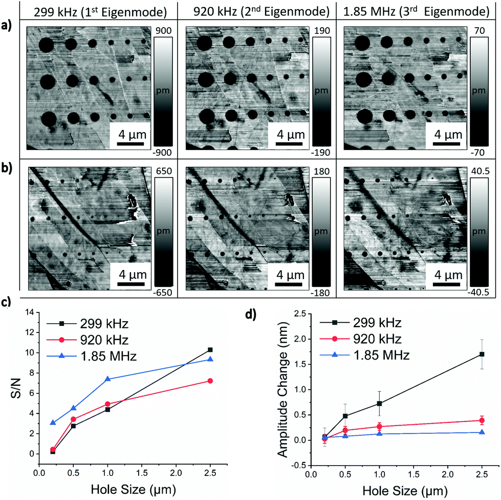 | ||
| Fig. 6 (a) AFAM amplitude images at various eigenmodes featuring hole sizes from 2.5 μm–800 nm and (b) 900 nm–100 nm. (c) Signal-to-noise ratio of the three eigenmodes at various hole sizes with its corresponding, (d) amplitude change. The cantilever used had a stiffness of 1.13 N m−1 (ASYELEC). | ||
From the S/N graph in Fig. 6c, the higher eigenmodes increase the subsurface contrast for the smaller holes. This is consistent with literature, in that higher eigenmodes should be more sensitive at a higher surface stiffness,34 which increases as the defect becomes smaller and less noticeable. Another possible explanation for the increased S/N ratio with higher eigenmodes is the reduction in thermal noise of the cantilever. Operating at the contact resonance itself likely makes the cantilever more susceptible to thermal vibrations, but it has also been shown that higher eigenmodes reduce the total amount of thermal noise experienced.35 The higher modes were not able to detect hole sizes smaller than 100 nm. To detect the smallest possible flaw, the drive frequency has been shown to have a larger impact than the various cantilever eigenmodes. A drive frequency of 10 kHz above the contact resonance peak is advised to reveal the smallest defects. Additionally, Fig. 6d shows a linear decrease in the amplitude contrast at 299 kHz even with larger hole sizes where the most acoustic scattering would take place, which confirms that the primary contrast mechanism is variations in the contact stiffness.
3.4. Effect of contact force and cantilever stiffness on subsurface defect detection
The non-destructive aspect of this technique is controlled by the contact force parameter, or the amount of force the tip is exerting on the sample. As this technique can be seen as a physical sensing technique, increasing the contact force has shown to improve the subsurface contrast, although the contrast quickly reaches a plateau with a further increase in force.12,14 To investigate contact force on subsurface defect detection, additional experiments were carried out on the same sample as the one used for determining the frequency dependence. Fig. 7 shows the influence of contact force at a drive frequency of 299 kHz.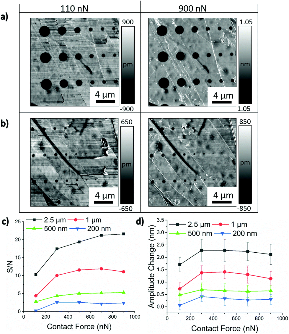 | ||
| Fig. 7 (a) AFAM amplitude images at 110 nN and 900 nN, featuring hole sizes from 2.5 μm–800 nm and (b) 900 nm–100 nm. (c) Signal-to-noise ratio of the various hole sizes at increasing contact force and the corresponding (d) amplitude change. The cantilever used had a stiffness of 1.13 N m−1 (ASYELEC). | ||
The S/N and amplitude change graphs in Fig. 7c and d are similar and agree with previous articles12,14 where initial increases of contact force improve the subsurface contrast. Further increases of force beyond 300 nN show no further improvement in contrast. Similar to varying eigenmodes, higher forces did not show the ability to detect hole sizes smaller than 100 nm, even at a contact force of 900 nN. In terms of defect depth detection, Ma et al., reported that increasing the contact force from 100 nN to 1000 nN would only result in a defect depth detection increase of approximately 13 nm.14 In the current graphite sample, it is possible to increase the contact force without causing any damage, however if this were a polymer system then there would likely be significant damage with such a large contact force.18 The final parameter we investigated was the effect of cantilever stiffness on subsurface defect detection. Using three cantilevers with a stiffness of 1.13, 2.89, and 21.8 nN nm−1 we applied the same contact force of 110 nN at drive frequencies 10 kHz above the contact resonance frequency and observed the subsurface contrast. While the S/N ratio was significantly enhanced using stiffer cantilevers for imaging the large 2.5 μm holes, the smaller holes showed minimal improvement (see Fig. S3 in section S4 in the ESI†). Similar to the higher eigenmodes, using a higher stiffness was reported to decrease the amount of thermal noise which might contribute to the reduced noise using a stiffer cantilever and thus higher S/N ratio for the larger holes.35
4. Conclusions
In summary, the detection limits of AFAM on subsurface defects were investigated on graphite flakes suspended over microcavities. AFAM was capable of imaging 2.5 μm diameter holes through a graphite thickness of 570 nm as well as imaging sub 100 nm diameter holes at a thickness of 140 nm. The smallest detectable defect size was a 50 nm hole buried under 80 nm of graphite. Increasing the graphite thickness and decreasing the hole diameters both exhibited the same trend of a decrease in the amplitude contrast. However, subsurface contrast decreased non-linearly for an increase in thickness while varying the defect size resulted in a linear relationship indicating that thickness has a much larger effect on AFAM's subsurface defect detection than variation in the defect size. Various parameters of AFAM such as drive frequency, cantilever eigenmodes, contact force, and cantilever stiffness were investigated with respect to their influence on defect detection. It was found that the optimal frequency for this setup was 10 kHz above the contact resonance frequency, whereas ±5 kHz of the peak showed very poor subsurface contrast. Utilizing higher cantilever eigenmodes resulted in improved subsurface defect contrast for smaller hole sizes. Initially increasing the contact force also showed an improvement in subsurface contrast, however above 300 nN the contrast plateaus. In both of these cases, while the contrast was improved, the smallest detectable hole size remained the same. Finally, using a stiffer cantilever was shown to significantly improve the subsurface contrast of much larger defects (2.5 μm) holes, but did little for the nanosized defects. In terms of depth detection, choosing the proper frequency is the most important factor in AFAM, whereas the other parameters only improved the contrast. Being able to resolve sub 100 nm defects in a stiff material such as graphite greatly increases AFAM's applicability as a NDT technique for nanostructured materials.Conflicts of interest
There are no conflicts of interest to declare.Acknowledgements
This work was funded by the Natural Sciences and Engineering Research Council of Canada (NSERC) oNDuTy CREATE program. In addition, we thank Clint Callahan at Asylum Research for his assistant in regards to software modifications. SEM images were obtained from the Advanced Micro and Nanosystems Laboratory (AMNL) and the Ontario Centre for the Characterization of Advanced Materials (OCCAM) at the University of Toronto.References
- K. J. Wolter, M. Oppermann and T. Zerna, 10th Electronics Packaging Technology Conference, EPTC 2008, 2008, vol. 873, pp. 873–878.
- A. Briggs and O. Kolosov, Acoustic Microscopy, Oxford University Press, 2009, p. 312 Search PubMed.
- R. F. Egerton, P. Li and M. Malac, Micron, 2004, 35, 399–409 CrossRef CAS PubMed.
- R. S. Gilmore, J. Phys. D: Appl. Phys., 1999, 29, 1389–1417 CrossRef.
- K. Yamanaka, H. Ogiso and O. Kolosov, Appl. Phys. Lett., 1994, 64, 178–180 CrossRef CAS.
- O. Kolosov, M. R. Castell, C. D. Marsh, G. A. D. Briggs, T. I. Kamins and R. S. Williams, Phys. Rev. Lett., 1998, 81, 1046–1049 CrossRef CAS.
- A. P. McGuigan, B. D. Huey, G. A. D. Briggs, O. V. Kolosov, Y. Tsukahara and M. Yanaka, Appl. Phys. Lett., 2002, 80, 1180–1182 CrossRef CAS.
- F. Dinelli, P. Pingue, N. D. Kay and O. V. Kolosov, Nanotechnology, 2017, 28, 85706 CrossRef PubMed.
- U. Rabe and W. Arnold, Appl. Phys. Lett., 1994, 64, 1493–1495 CrossRef.
- U. Rabe, S. Amelio, M. Kopycinska, S. Hirsekorn, M. Kempf, M. Göken and W. Arnold, Surf. Interface Anal., 2002, 33, 65–70 CrossRef CAS.
- A. Striegler, B. Koehler, B. Bendjus, M. Roellig, M. Kopycinska-Mueller and N. Meyendorf, Ultramicroscopy, 2011, 111, 1405–1416 CrossRef CAS PubMed.
- J. P. Killgore, J. Y. Kelly, C. M. Stafford, M. J. Fasolka and D. C. Hurley, Nanotechnology, 2011, 22, 175706 CrossRef PubMed.
- S. Hu, C. Su and W. Arnold, J. Appl. Phys., 2011, 109, 084324–084324 CrossRef.
- C. Ma, Y. Chen, W. Arnold and J. Chu, J. Appl. Phys., 2017, 121, 154301–154301 CrossRef.
- G. S. Shekhawat and V. P. Dravid, Science, 2005, 310, 89–92 CrossRef CAS.
- L. Tetard, A. Passian and T. Thundat, Nat. Nanotechnol., 2010, 5, 105–109 CrossRef CAS PubMed.
- H. J. Sharahi, G. Shekhawat, V. Dravid, S. Park, P. Egberts and S. Kim, Nanoscale, 2017, 9, 2330–2339 RSC.
- G. J. Verbiest, T. H. Oosterkamp and M. J. Rost, Nanotechnology, 2017, 28, 085704 CrossRef CAS PubMed.
- K. Kimura, K. Kobayashi, K. Matsushige and H. Yamada, Ultramicroscopy, 2013, 133, 41–49 CrossRef CAS PubMed.
- S. A. Cantrell, J. H. Cantrell and P. T. Lillehei, J. Appl. Phys., 2007, 101, 114324–114324 CrossRef.
- K. Yamanaka, Thin Solid Films, 1996, 273, 116–121 CrossRef CAS.
- T. Tsuji and K. Yamanaka, Nanotechnology, 2001, 12, 301–307 CrossRef CAS.
- T. Wang, C. Ma, W. Hu, Y. Chen and J. Chu, Microsc. Res. Tech., 2017, 80, 66–74 CrossRef CAS.
- N. Gomopoulos, W. Cheng, M. Efremov, P. F. Nealey and G. Fytas, Macromolecules, 2009, 42, 7164–7167 CrossRef CAS.
- O. L. Blakslee, D. G. Proctor, E. J. Seldin, G. B. Spence and T. Weng, J. Appl. Phys., 1970, 41, 3373–3382 CrossRef CAS.
- W. Zhang, Y. Chen, H. Liu and L. Zheng, Appl. Phys. Lett., 2018, 113, 193105–193105 CrossRef.
- U. Rabe, Applied scanning probe methods II: scanning probe microscopy techniques, 2006, pp. 37–90 Search PubMed.
- Z. Parlak and F. L. Degertekin, J. Appl. Phys., 2008, 103, 114910–114910 CrossRef.
- G. J. Verbiest, J. N. Simon, T. H. Oosterkamp and M. J. Rost, Nanotechnology, 2012, 23, 145704 CrossRef CAS PubMed.
- A. Castellanos-Gomez, M. Poot, G. A. Steele, H. S. J. Van Der Zant, N. Agraït and G. Rubio-Bollinger, Adv. Mater., 2012, 24, 772–775 CrossRef CAS PubMed.
- U. Komaragiri, M. R. Begley and J. G. Simmonds, J. Appl. Mech., 2005, 72, 203 CrossRef.
- M. H. van Es, A. Mohtashami, R. M. Thijssen, D. Piras, P. L. van Neer and H. Sadeghian, Ultramicroscopy, 2018, 184, 209–216 CrossRef CAS PubMed.
- C. Ma, Y. Chen and T. Wang, AIP Adv., 2015, 5, 027116–027116 CrossRef.
- J. A. Turner and J. S. Wiehn, Nanotechnology, 2001, 12, 322–330 CrossRef.
- H. J. Butt and M. Jaschke, Nanotechnology, 1999, 6, 1–7 CrossRef.
Footnote |
| † Electronic supplementary information (ESI) available. See DOI: 10.1039/C9NR03730F |
| This journal is © The Royal Society of Chemistry 2019 |