
 Open Access Article
 This Open Access Article is licensed under a Creative Commons Attribution-Non Commercial 3.0 Unported Licence
Sculpturing wafer-scale nanofluidic devices for DNA single molecule analysis†
Franziska M.
Esmek‡
a,
Parisa
Bayat‡
a,
Fabián
Pérez-Willard
b,
Tobias
Volkenandt
b,
Robert H.
Blick
a and
Irene
Fernandez-Cuesta
 *a
*a
aInstitut für Nanostruktur- und Festkörperphysik (INF)/Center for Hybrid Nanostructures (CHyN), University of Hamburg, Luruper Chaussee 149, 22761 Hamburg, Germany. E-mail: ifernand@physnet.uni-hamburg.de
bCarl Zeiss Microscopy GmbH, Carl-Zeiss-Str. 22, 73447 Oberkochen, Germany
First published on 2nd July 2019
Abstract
We present micro- and nanofluidic devices with 3D structures and nanochannels with multiple depths for the analysis of single molecules of DNA. Interfacing the nanochannels with graded and 3D inlets allows the improvement of the flow and controls not only the translocation speed of the DNA but also its conformation inside the nanochannels. The complex, multilevel, multiscale fluidic circuits are patterned in a simple, two-minute imprinting step. The stamp, the key of the technology, is directly milled by focused ion beam, which allows patterning nanochannels with different cross sections and depths, together with 3D transient inlets, all at once. Having such a variety of structures integrated in the same sample allows studying, optimizing and directly comparing their effect on the DNA flow. Here, DNA translocation is studied in long (160 µm) and short (5–40 µm) nanochannels. We study the homogeneity of the stretched molecules in long, meander nanochannels made with this technology. In addition, we analyze the effect of the different types of inlet structures interfacing short nanochannels. We observe pre-stretching and an optimal flow, and no hairpin formation, when the inlets have gradually decreasing widths and depths. In contrast, when the nanochannels are faced with an abrupt transition, we observe clogging and hairpin formation. In addition, 3D inlets strongly decrease the DNA molecules’ speed before they enter the nanochannels, and help capturing more DNA molecules. The robustness and versatility of this technology and DNA testing results evidence the potential of imprinted devices in biomedical applications as low cost, disposable lab-on-a-chip devices.
Introduction
New micro- and nanofabrication technologies are leading the way for the development of portable devices. These allow for in situ detection and quantification of a variety of analytes, like iron in blood,1 gases in a combustion engine, or toxins in fresh water.2 But there are still challenges to address, like expanding the range of (bio)molecules that can be detected, improving the device sensitivity to study single molecules, and reducing the fabrication costs to make the devices affordable.Integrated micro- and nanofluidic devices are valuable tools for handling, manipulating and detecting ultra-low quantities of biomolecules.3–5 In particular, on-chip analysis of DNA6,7 can have an impact on early disease diagnosis, on personalized medicine and on effective cancer treatment.8 The DNA molecules can be stretched inside nanochannels and analyzed, for instance, by optical mapping.9–12,41
Physical confinement13 of the molecules in the nanochannels is a reliable and reproducible elongation method.14,15 And decreasing the nanochannel cross-section reduces the conformational degree of freedom, so the DNA molecules can be elongated to almost their full contour length.15–17 But the smaller the cross section, the larger the size mismatch between micro and nanostructures, and the harder it gets for the DNA to overcome the entropic barrier and enter the nanochannel. This becomes especially problematic for very long molecules (e.g., genomic length DNA15), which often get entangled and clog the entrance of the nanochannels. In this respect, structures like pillars with gradually decreasing size can be patterned in the microchannels to ease the introduction of genomic DNA into nanochannels.18,19 These structures also pre-stretch the DNA and solve the problem of hairpin formation. Another solution is to gradually decrease the dimensions of the micro or nanochannel to smoothen the transition. Structures with not only gradually decreasing widths but also depths (i.e., “funnel”-like) are optimal for this purpose,20 but their fabrication is time-consuming and complicated. Since these inlets require a gradient depth profile, standard 2D top down techniques need to be tuned, or alternative methods need to be used, and every additional processing step translates into additional fabrication time for each sample.
Genomic length DNA molecules can be visualized for example in long, meander nanochannels21 or studied using a point-light source and a photon counter in shorter nanochannels.22 In both cases, the inlets play an important role. For the long nanochannels, for an optimal stretching, the cross section needs to have a comparable dimension to the DNA persistence length, which is in the order of 50 nm. This results in a large entropic barrier, and only by using graded structures and/or inlets it is possible to bring the molecules in the channel. In the second case, when the length of the nanochannels is similar or shorter than the length of the stretched DNA, the molecules do not have time to relax,23 and often form hairpins24 when they enter the nanochannels, preventing a good quality of the read-out signal. By using appropriate inlets, the molecules can be pre-stretched to avoid the hairpin formation and have an optimal, linear conformation inside the nanochannel.
Patterning of fluidic structures with controlled positions, depths and dimensions requires top-down fabrication methods, and usually several micro- and nano lithography steps.25–31 Most of the techniques used now-a-days suffer from limitations, especially when the patterning involves both micro and nanostructures and funnel structures.32 Nanoimprint lithography is a parallel, high throughput mechanical molding process, where the structures on the stamp are physically imprinted into a polymer film at wafer scale with high throughput and resolution.33–35 The fabrication of stamps is a crucial process of this technology, since the quality of the final structures directly depends on the quality of the stamp. Stamps for making devices requiring different depths, as would be ideal for the fluidic devices used for genomic-length DNA stretching, are particularly complex, and the associated stamp fabrication is challenging.
Here, we propose a combination of direct milling by focused ion beam (FIB) for rapid prototyping of master stamps and ultraviolet nanoimprint lithography (UV-NIL) for high throughput device fabrication.
FIB direct milling enables maskless and resist-free fabrication of nanostructures with different cross sections and depth levels, all in one step.36 And, as an especially interesting point, 3D patterning is straightforward and is very useful for fabricating devices with nanochannels with transient and funnel inlets for DNA stretching. This is not possible with other techniques.
However, FIB milling is slow and has a low throughput. In order to overcome its limitations and compensate for the costs, once the silicon stamp is fabricated, we use direct nanoimprinting to make the devices using the FIB-made structures for imprinting. In this way, the fluidic samples are fabricated at wafer scale, in parallel, in a two-minute process. Since we use the polymer as an active material, there is no need for post-processing, and the samples can be directly used afterwards for flow tests. Thus, the combination of FIB and UV-NIL leads to a fast and simple “nano-sculpturing” of multilevel, multidimensional lab-on-a-chip devices for biomedical applications.
The simplicity of the fabrication process, biocompatibility of the polymer, and the optical transparency of the micro- and nanochannels for flow visualization are key characteristics of this approach.
In this article, we demonstrate how FIB allows simple patterning of stamps with multiple depth levels and 3D structures. Subsequently, we show the quick imprinting of the stamp structures into fluidic devices. We study the flow and stretching of λ-DNA molecules in different types of nanochannels. We characterized the homogeneity of the elongated molecules in 160 μm long, meander nanochannels. And we studied the effect of the topography on the flow of DNA molecules in nanochannels with shorter lengths (between 5 and 40 μm). We compared the flow along similar nanochannels interfaced with different inlet geometries, with 3D structures, transient nanochannels and other configurations, and compared them with abrupt micro-to-nano transitions. We characterized the flow time from one microchannel to the other, the pre-stretching and the translocation speed and conformation inside the nanochannel. We found the best configurations to avoid coiled or hairpin-shaped DNA inside the nanochannels.
Results and discussion
Fabrication process
Fig. 1 shows a schematic overview of a 1 cm × 1 cm stamp to make fluidic devices. It has two U-shaped microchannels, which connect four liquid reservoirs to the nanochannels. Nanochannels with different depths and cross sections run perpendicular to the microchannels, and tapered inlets connect the micro- and nanostructures.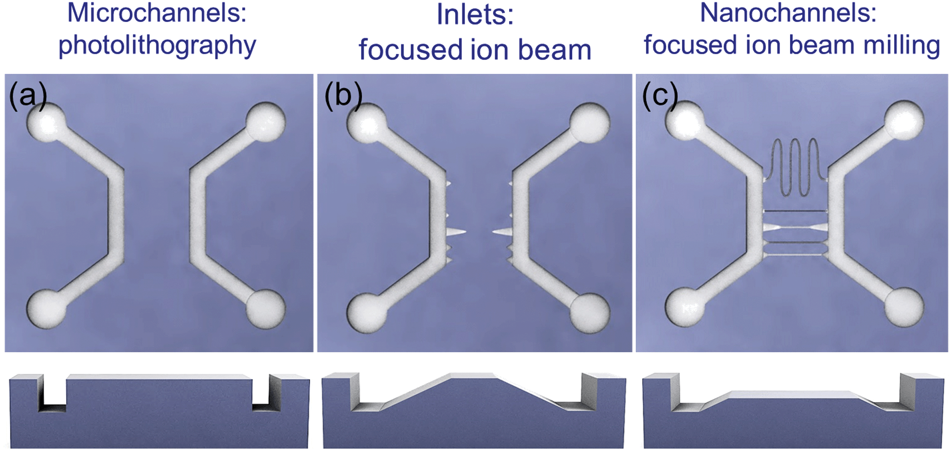 | ||
| Fig. 1 Sketch of the silicon stamp fabrication. (a) Microchannels are fabricated by photolithography and reactive ion etching. (b) Transient inlets are milled by focused ion beam. (c) Nanochannels are milled also by focused ion beam milling. Different types of nanochannels (linear and meander, with different widths and depths) and different inlets (graded, 3D, stepped) can be milled in the same step. | ||
The device fabrication is based on a double imprint process.37 First, a silicon master stamp is fabricated by FIB and photolithography. Then, a negative replica is made by UV nanoimprint lithography, so all micro- and nanofeatures of the silicon stamp are transferred into the polymeric copy at once. Afterwards, this negative stamp is used as a working stamp to imprint the fluidic devices again by UV-NIL.
In this work, the silicon master stamp is fabricated in two steps, as sketched in Fig. 1. First, the microchannels are made by conventional photolithography, followed by dry etching, as shown in Fig. 1(a). The detailed process and parameters are described in the ESI.† In all stamps of this work, the microchannels are ∼20 µm wide and ∼1 µm deep. Then, multilevel transient inlets and nanochannels with different depths and profiles are directly milled by FIB (Zeiss Crossbeam 550) as shown in Fig. 1(b) and (c) respectively. A video showing the milling of a channel and the 3D inlets is attached as ESI media.†
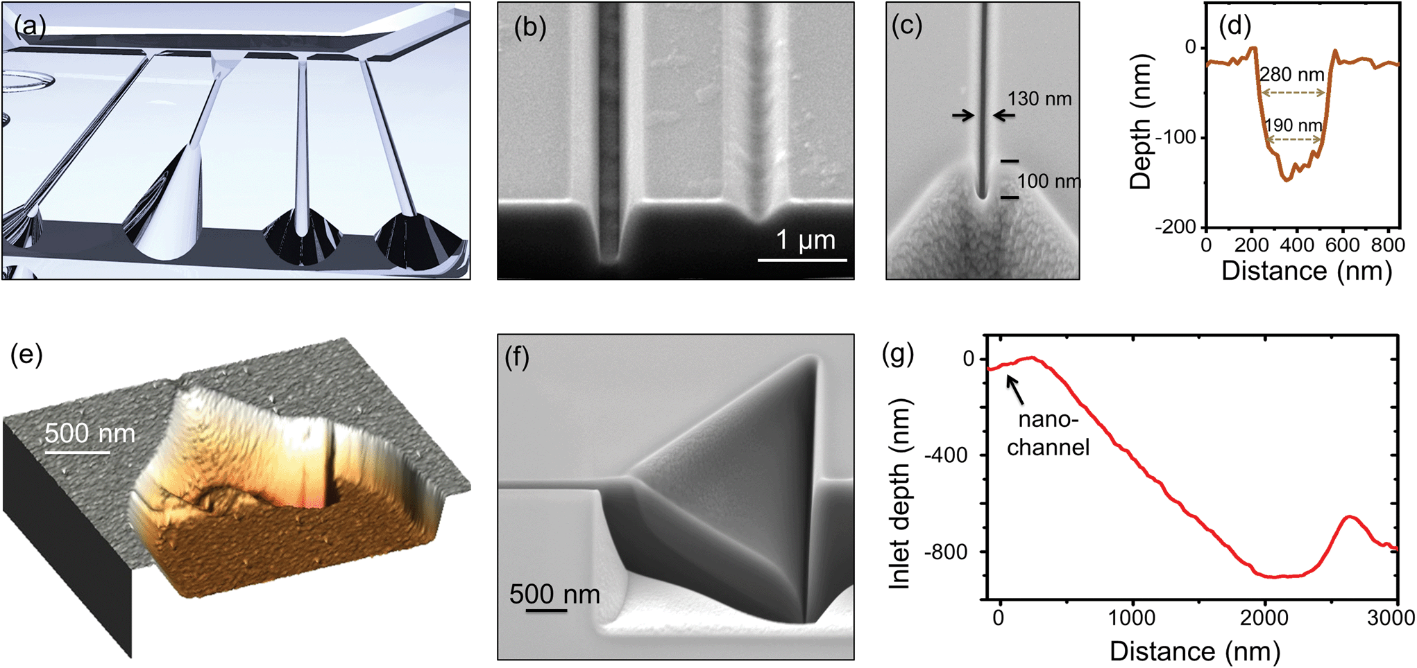 | ||
| Fig. 2 (a) 3D sketch of nanochannels with different lengths, cross sections and depths in a device. (b) SEM image of the cross section of two nanochannels with different depths and profiles. The deeper, U-shaped nanochannel on the left is milled with a three times higher current than the shallower, V-shaped nanochannels on the right, as explained in the text. (c) SEM image of a nanochannel, 130 nm wide and 100 nm deep, connected to a 3D funnel inlet. (d) AFM profile of a nanochannel; it has a FWHM of 280 nm and is 120 nm deep. The sidewall angle is 75°. (e–g) 3D funnel-like tapered inlets. (e) Shows an AFM image of the inlet. (f) Is an SEM image of an inlet cross section. (g) Shows the profile and slope of a 3D inlet. The milling time for one inlet is 40 seconds. The slope angle is 30°. The AFM images and profiles in (d), (e) and (g) are taken from the negative polymeric replica, so the nanochannels are protruded. Then the profiles are inverted. This minimizes the tip convolution, and ensures the accuracy of the measured height/depth. | ||
Using a FIB-SEM system allows imaging the process in real time, which leads to a quick and easy quality control during parameter optimization. Thanks to this, nanochannels as small as 130 nm × 100 nm can be achieved, as shown in Fig. 2(c). However, we never observed DNA flow inside such small nanochannels. On the other hand, nanochannels with lateral dimensions starting at 180 nm could be successfully used for DNA flow.
Fig. 2(d) shows the AFM profile of a nanochannel to study the conservation of the critical dimensions, the slope of the walls and the roughness. It has a FWHM of 280 nm and a depth of 120 nm. Square-shaped nanochannels are typically 30% wider at the top than at the bottom, and have a sidewall slope angle of 75°. The measured wall roughness is between 10 and 12 nm, as calculated from the AFM images.
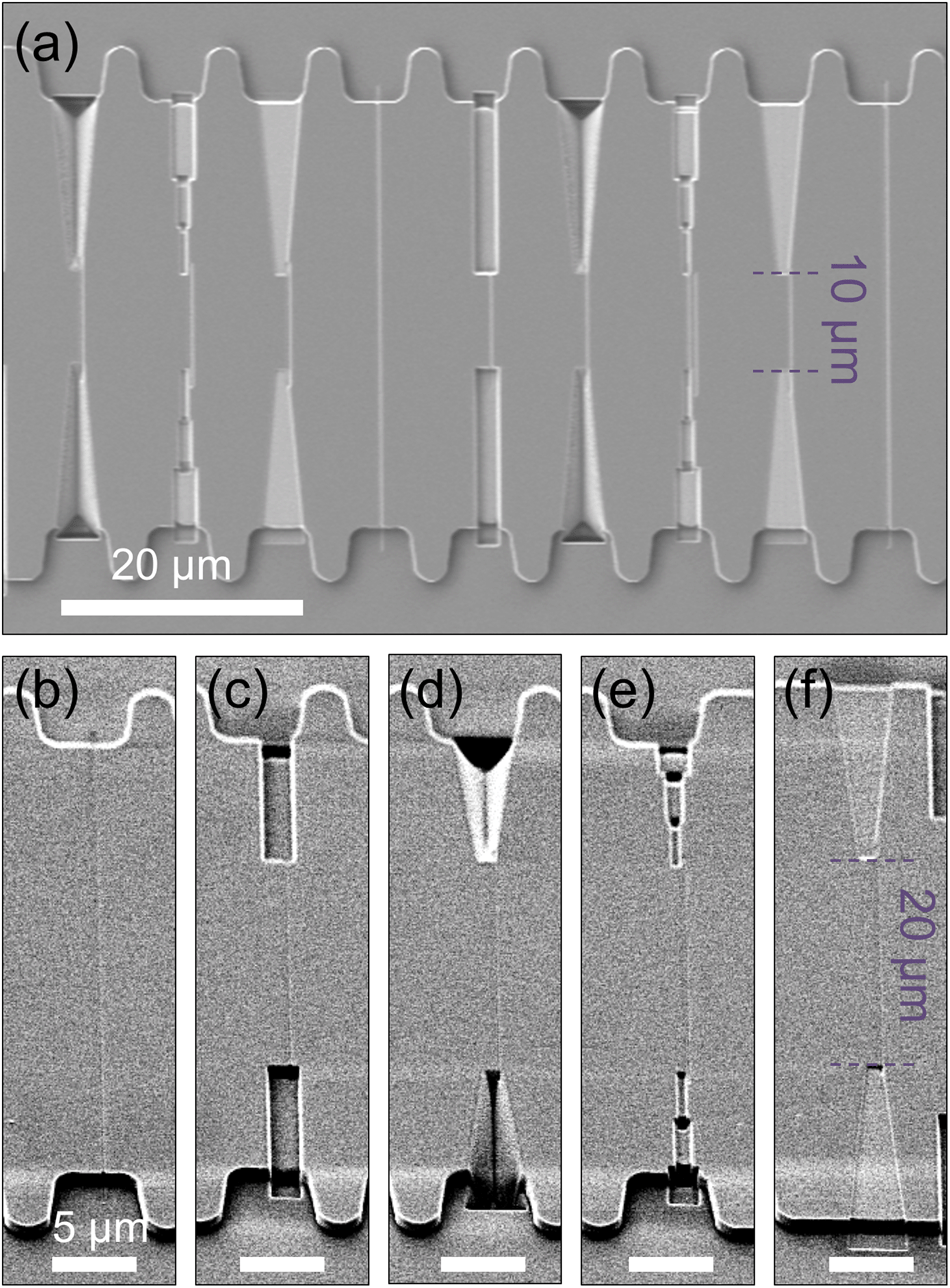 | ||
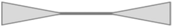
| Fig. 3 Silicon stamp with nanochannels connected to the microchannels using different types of inlets, milled by focused ion beam. (a) General overview of the stamp. (b)–(f) Examples of the different types of inlets. A long, straight nanochannel directly connected to the microchannel (no inlet) is shown in (b). An abrupt transition is shown in (c), where the nanochannel is connected to a 2 μm wide, 1 μm deep inlet. A smooth, 3D inlet is shown in (d). Transient nanochannels, gradually narrower and shallower are shown in (e). The first channel is 2 µm wide and 1 µm deep; the second one is 1 µm wide and 600 nm deep; and the third one is 500 nm wide and 400 nm deep. And a shallow, flat, triangular inlet can be seen in (f), which is 220 nm deep. All the nanochannels in (b)–(f) are 260 nm wide and 220 nm deep, and they are all integrated in the same stamp, one after the other. | ||
Another stamp was made, following the same idea of comparing the different transient elements (squared channels with micro to nano dimensions and 3D inlets), combined in blocks. SEM images of the stamp and details of the idea can be found in the ESI.†
 | ||
| Fig. 4 (a) Image of a stamp with an array of four similar meander nanochannels, ∼158 μm long, ∼350 nm wide, and ∼150 nm deep. The total milling time for this stamp, including the nanochannels and inlets is less than 8 minutes. (b–d) Double replication process: a sketch of the silicon stamp is shown in (b), of the negative replica in (c) and of the final fluidic device in (d). (e–j) SEM images of a meander nanochannel and close-ups. (e, h) Show the nanochannels in the silicon master stamp and (f, i) in a transparent negative replica made by UV-NIL. (g, j) Show the channel in the polymeric fluidic device, imprinted by UV-NIL using the sample as shown in (e) as the stamp. The SEM images are taken using charge compensation, with no metal coating, also for the polymer-on-glass devices. | ||
Fig. 4(e–j) show scanning electron microscopy (SEM) images of the structures along the double imprinting process, for a nanochannel in the silicon stamp ((e) and (h)), in a negative replica polymer stamp ((f) and (i)) and in the final polymer fluidic sample ((g) and (j)). As can be seen, the quality and smoothness of the imprinted micro and nanostructures is replicated from the original silicon stamp across the different steps. Both the silicon stamp and the negative stamp can be reused several times to fabricate hundreds of samples.
To perform flow measurements on the final fluidic device, the sample needs to be sealed. A glass coverslip and the sample are brought into contact and bonded just by pushing them together with the fingers. The presence of –OH groups on the surface of the polymer is the key for the adhesion and proper sealing.40 Fluid flow experiments are performed to validate the patency and continuity of the nanochannels and the liquid confinement. (Micro)spectroscopy measurements also verify and examine the sealing quality, and discard possible leaks arising from FIB unspecific milling. These measurements are shown in the ESI.† In addition, to show that the fabrication process is versatile and the devices can be used for other applications, we also show the confinement and characterization of individual quantum dots in the imprinted devices in the ESI.†
Stretching of DNA molecules in the nanochannels
DNA molecules have typically a coiled conformation in solution. It is thermodynamically unfavourable for them to spontaneously enter the nanochannels. To facilitate the flow, we work on two sides. On the one hand, the transient inlets at the entrance of the nanochannels are designed to overcome the size mismatch between micro- and nanochannels. On the other hand, we can apply a voltage gradient between the opposite microchannels to drive the molecules into the nanochannels by electrophoresis.We have fabricated different types of devices: with long (160 µm) meander nanochannels, and with short (5–20 µm) linear nanochannels. For this work, we used λ-DNA stained with YOYO-1 in a ratio of 1![[thin space (1/6-em)]](https://www.rsc.org/images/entities/char_2009.gif) :5 dyes per base pair. Under these conditions, the contour length of the molecules (LDNA) is ∼20 µm.17 In this context, and for the sake of simplicity, we refer in the following to “long nanochannels” as those with a length (Lnch) longer than the contour length of the DNA molecules (Lnch ≫ LDNA), so the stretched molecules fully fit inside, and can be imaged several times with a camera as they flow through. On the other hand, we use the term “short nanochannels” for those whose length is similar or shorter than the DNA contour length (Lnch ≤ LDNA).
:5 dyes per base pair. Under these conditions, the contour length of the molecules (LDNA) is ∼20 µm.17 In this context, and for the sake of simplicity, we refer in the following to “long nanochannels” as those with a length (Lnch) longer than the contour length of the DNA molecules (Lnch ≫ LDNA), so the stretched molecules fully fit inside, and can be imaged several times with a camera as they flow through. On the other hand, we use the term “short nanochannels” for those whose length is similar or shorter than the DNA contour length (Lnch ≤ LDNA).
In both cases, the transient inlets are necessary for a smooth flow, to bring the molecules uncoiled into the nanochannels and avoid clogging, as explained before. The meander nanochannels are long and have a small cross section for an optimal physical confinement, what makes the entry of the DNA molecules challenging. The 3D inlets patterned at the entrance help to overcome this barrier. In short nanochannels the stretching is dynamic and fast (i.e., one end pulls from the rest of the molecule). Since the molecules do not have time to relax,23 they often form clogs or hairpins when they enter the nanochannels,24 preventing a good quality of the read-out signal. By using appropriate inlets, the molecules can be pre-stretched to avoid the hairpin formation, as will be shown in this work.
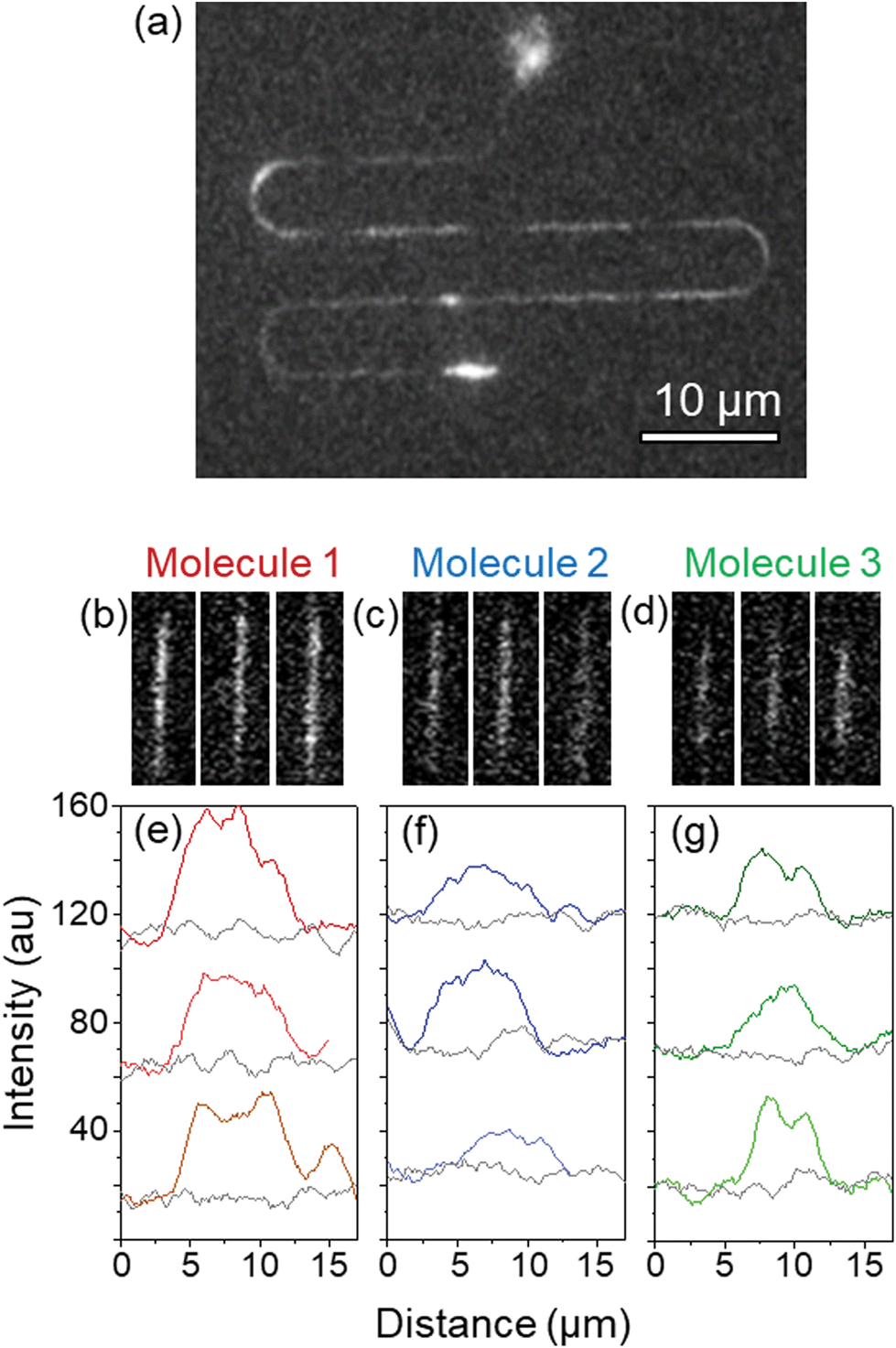 | ||
| Fig. 5 Stretching of λ-DNA molecules in a 160 µm long, meander nanochannel driven by electrophoresis. (a) Shows a projection of the maximum fluorescence intensity of each pixel, obtained from a 140 frame movie. The movie frames are shown in the ESI,† and the video is attached as supplementary media. It shows several molecules flowing through the nanochannel. The fluorescence intensity profiles of three of these molecules (molecules 1, 2 and 3) have been measured at three different positions of the same nanochannel. (b)–(d) Show the fluorescence images and (e)–(g) show the corresponding intensity profiles. The apparent length values and the averages are summarized in Table 1. | ||
We have evaluated the homogeneity of the elongation of the molecules, since this is a direct measurement of the homogeneity of the lateral dimensions of the nanochannels fabricated following the process presented here. For this, we have measured the fluorescence profile of one specific molecule (“Molecule 1”) at three different positions of the meander nanochannel. Fig. 5(b) shows fluorescence images of this molecule at the three positions, and (e) shows the corresponding intensity profiles. Similar measurements for two other molecules (“Molecule 2” and “Molecule 3”) can be seen in Fig. 5(c)–(g). The values of the apparent lengths for each molecule and position, and their averages are summarized in Table 1. These results show that each molecule is homogeneously stretched inside the nanochannel, with a variation in the order of 3 to 5%.
| Apparent length (μm) | |||
|---|---|---|---|
| Molecule 1 | Molecule 2 | Molecule 3 | |
| Position 1 | 10.1 | 8.7 | 7.1 |
| Position 2 | 10.6 | 8.6 | 8.1 |
| Position 3 | 9.5 | 10.1 | 6.8 |
| Average | 10.1 ± 0.3 | 9.2 ± 0.4 | 7.3 ± 0.4 |
We have flown λ-DNA molecules into such devices, and recorded the translocation of the molecules by fluorescence microscopy. Two videos with the live translocation of the DNA molecules along devices where the nanochannels are interfaced with the different types of inlets can be seen in the ESI media.† One shows a device imprinted using the stamp shown in Fig. S6,† and the other using the stamp shown in Fig. 3. Fig. 6 shows a summary of the molecule flow from the bottom microchannel to the upper one: the molecules enter into the different inlets with different geometries, get stretched in the nanochannels, and then from the outlet into the upper microchannel. A time sequence of one molecule flowing in a long nanochannel without inlets is shown in (a), in a nanochannel with an abrupt transition in (c), in a nanochannel interfaced with a set of transient nanochannels, gradually smaller and shallower, in (d), and in a nanochannel with a long, smooth, 3D inlet in (b). All the nanochannels are part of the same sample, can be found one next to each other, and all the images correspond to the same experiment. For each configuration, a sketch of the configuration is shown, together with an SEM image of the actual structure, and a series of fluorescence images (consecutive, 100 ms apart), showing the translocation of a DNA molecule from one microchannel to the opposite one. The graph in Fig. 6(e) shows the position of the molecules along the inlets and nanochannels vs. time obtained from the fluorescence images for each configuration.
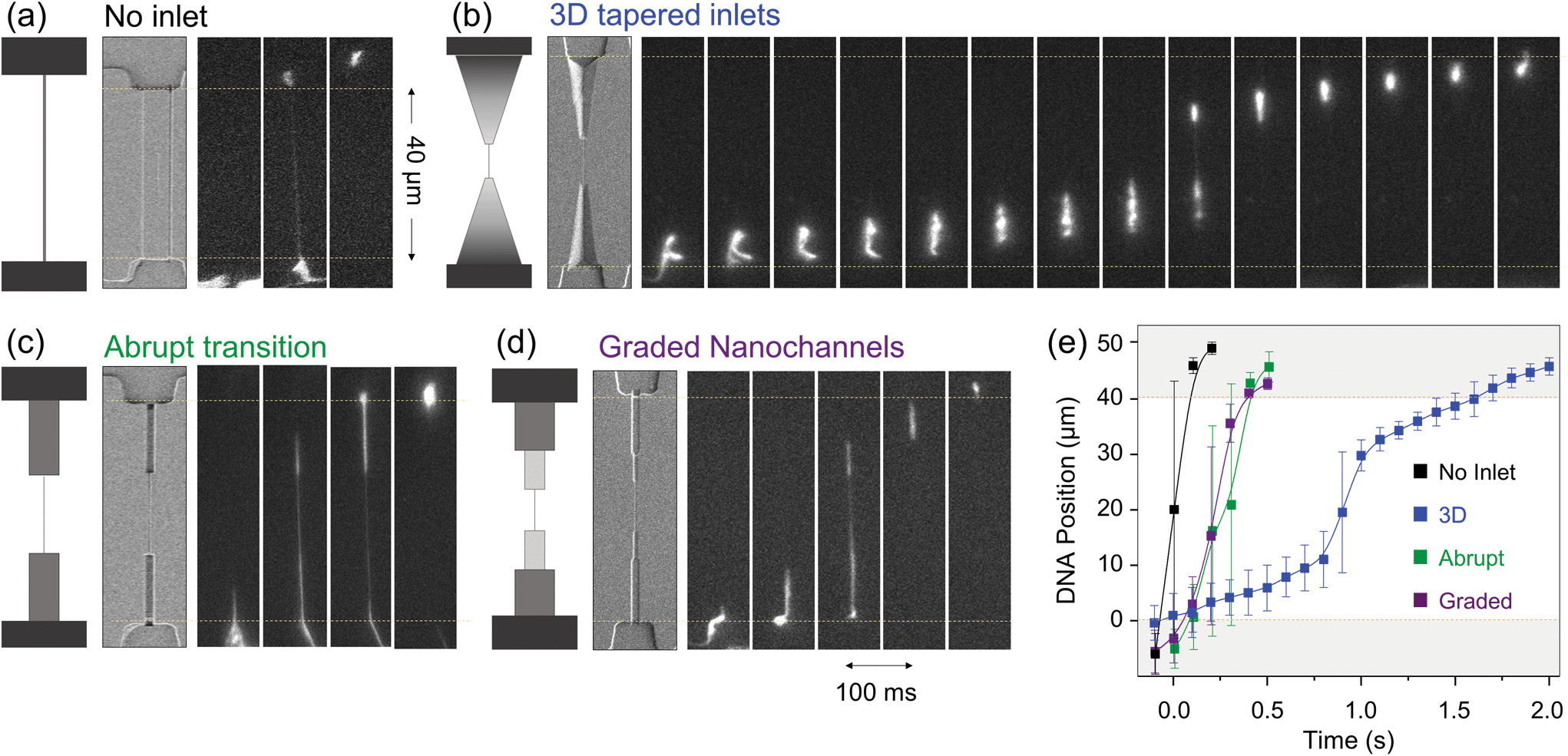 | ||
| Fig. 6 λ-DNA flow in nanochannels with different types of inlets in the same sample. For each configuration, a sketch of the geometry can be seen, a SEM image of the channel, and a series of consecutive fluorescence images, 100 ms apart, showing the translocation of one DNA molecule. The flow in real time can be seen in a video in the ESI.† (a) Shows the flow of a λ-DNA molecule in a long nanochannel without inlets. (b) Shows the flow in a nanochannel connected to smooth, 3D tapered inlets. (c) Shows a nanochannel accessed with a 1 μm wide and 1 μm deep channel, reflecting an abrupt micro-to-nano transition. (d) Shows a set of nanochannels with gradually decreasing depths and widths. (e) Representation of the position of the DNA molecules along the nanochannel and inlets vs. time for the different configurations shown in (a)–(d). The error bars represent the molecule elongation, and the squares the central position of the molecule. The temporal separation between points, as in the images, is 100 ms. The distance between one microchannel and the other is 40 μm. The translocation times from one microchannel to the other are very different depending on the inlet configuration, as shown also in Table 1. The conformation of the DNA molecules inside each channel is different too, as shown in Fig. 7. | ||
Several things can be evaluated for each inlet type: the flow time from one microchannel to the other, the pre-stretching (both have an effect on the hairpin formation, and to avoid clogging) and its effectiveness for capturing DNA molecules (which will increase the number of molecules that flow through the nanochannels).
Microchannel to microchannel flow time. The time sequences shown in Fig. 6(a)–(d) and the graph in (e) show the time that the molecules need for flowing from one microchannel to the other. This time is increased by the presence of the inlets and it depends on their geometry. The molecules flow from the bottom microchannel up to the opposite one in less than 100 ms when they flow through the nanochannels without inlets. In squared, deep inlets, the molecule flows from the microchannel, into the inlet, through the nanochannel, and out of the outlet in 400 ms. On the other hand, when the inlet has a 3D funnel shape, the molecule needs 1.5 s to travel the same path. In this respect, it could be said that the long, 3D tapered inlets “slow down” the molecules before they enter the nanochannels.
Pre-stretching and hairpin formation. DNA clogs the entrance of nanochannels when the centre of the molecule is pulled into the nanochannel, instead of one of the ends. The longer the molecule, the more likely this is to happen. In the case where the cross section of the nanochannel is smaller than the effective section of the coiled molecule, this results in clogging. When the cross section is larger, the molecule can enter the nanochannels and flow through, but it will have a hairpin conformation, instead of being elongated. Both clogging and hairpin formation can be avoided by using appropriate inlets, which pre-stretch the molecule and thus facilitate that one end finds the entrance first.
Using a laser focused into the nanochannel as a point-excitation and a photon counter as a real time fluorescence read out, we can gain insight into the conformation of the molecules inside short nanochannels.24Fig. 7 shows the real time fluorescence signals of several λ-DNA molecules translocating through short nanochannels interfaced with different inlet configurations: an abrupt transition (a), squared transient inlets (b), and smooth 3D inlets (c). The three graphs have the same x and y scales, for a reliable comparison. These channels correspond to those shown before in Fig. 6(b), (c) and (d), and the configuration is sketched again inside each graph.
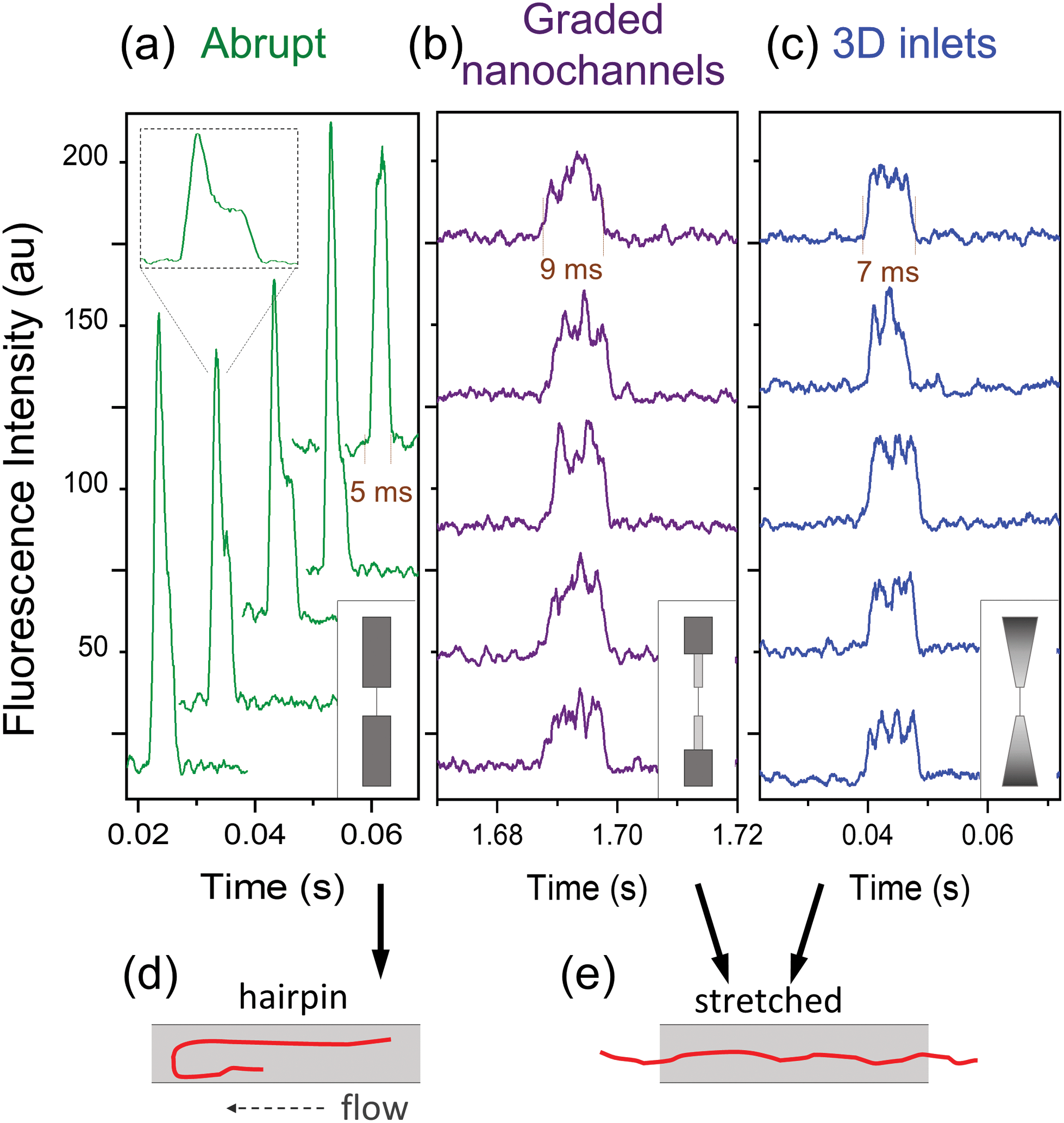 | ||
| Fig. 7 Real time photoluminescence signals of λ-DNA molecules translocating through three similar nanochannels, interfaced with different inlets. (a) Shows the fluorescence bursts of DNA molecules flowing through a 280 nm nanochannel connected to a 1 μm wide and 1 μm deep inlet. This represents an abrupt transition. (b) Shows the molecules flowing through a nanochannel connected to gradually narrower and shallower inlets. (c) Shows the DNA translocation through a nanochannel connected to 3D funnel-like inlets. The channels in (b) and (c) are identical: 250 nm wide, 5 μm long. Each graph shows the signals of five different molecules. The measurements were obtained from nanochannels in the same sample, one after the other, so the intensity values can be quantitatively compared. The molecules in the abrupt transition configuration in (a) have a hairpin conformation, as can be concluded from the PL signal shape, highlighted in the inset, while those in the smooth transitions are fully elongated. (d) and (e) Show a sketch for the two situations. The average translocation times are summarized in Table 2. | ||
The configuration with an abrupt micro- to nanochannel transition results in hairpin formation inside the nanochannel, as evidenced from the signals in Fig. 7(a) and as sketched in (d). In the inset on the top it can be seen that the signals are intense at the beginning, corresponding to the coiled part of the molecule, and then the intensity becomes lower and constant, corresponding to the stretched part.
For the cases of smooth transitions, either by using nanochannels with gradually smaller cross sections (Fig. 7(b)) or a 3D inlet (Fig. 7(c)), the DNA signals have a step shape, with homogeneous intensity and duration, as a result of linearly stretched molecules inside the nanochannel, without coils or hairpins, as sketched in Fig. 7(e). Thanks to the slowing down of the molecules and to the gradually decreasing dimensions, the 3D inlets and the rectangular, graded ones do pre-stretch the molecules, compared to straight nanochannels without inlets or those with an abrupt transition.
Table 2 shows the average peak durations and the calculated translocation speeds for the three different configurations, measured from the real time fluorescence signals obtained with the laser excitation. The signals appear shorter for the abrupt transition (5 ms) as a result of the coil and become longer for the smooth transitions: 8.8 ms for the graded nanochannels, and 7.1 ms for the 3D inlets. The DNA shows a similar elongation in both cases (the signals in (b) and (c) have similar intensities) but translocates slightly faster in the nanochannels with the 3D inlets (5.51 ± 0.69 kbp ms−1vs. 6.83 ± 0.67 kbp ms−1). This proves that the topography has a clear effect not only on the conformation but also on the speed of the DNA inside the short nanochannels, since both compared nanochannels are identical (the same cross section and length) and just the inlets are different.
| Inlet type | Average peak duration (ms) | Average translocation speed (kbp ms−1) | Conformation of DNA inside |
|---|---|---|---|
| Abrupt | 4.9 ± 0.8 | 9.9 ± 1.6 | Hairpin |
| Graded | 8.8 ± 1.1 | 5.5 ± 0.7 | Stretched |
| 3D | 7.1 ± 0.7 | 6.8 ± 0.7 | Stretched |
Capturing DNA. The number of molecules translocating through the nanochannel for a given time frame is another important aspect to consider. It depends on the DNA concentration in the microchannel and on the ability of the inlet to “capture” the molecules. The electro-osmotic forces across the nanochannel act only on those molecules that flow near the entrance. Having an inlet already improves significantly the capturing volume, since the cross section interfacing the microchannel is strongly increased, not only in the horizontal plane but also in depth. Then, the forces push the molecule into the nanochannel, provided it is enough to overcome the entropic barrier.20 In this respect, 3D or graded inlets smoothen the entropic barrier for the molecules, thus reducing the force opposing the flow, and improve the capturing rate.
We study how many molecules flow into each nanochannel configuration per minute, as a measure of the ability of the different inlets to capture DNA. We used samples imprinted with the stamp presented in Fig. 3, where all the channels have the exact same lateral dimensions and lengths (260 nm wide, 220 nm deep, and 20 μm long), and only the inlets are different. A video of the flow in real time is attached as supplementary media.
The number of DNA molecules that flow through each nanochannel per minute for each configuration is summarized in Table 3. Three cases similar to those analysed before are shown: an abrupt transition, a 3D inlet, and a nanochannel interfaced with gradually smaller squared nanochannels. In addition, we also show a shallow, 2D triangular inlet and a 40 µm long nanochannel directly connected to the microchannel without inlets. The molecules were counted from several consecutive videos, where the understudied channels were all simultaneously observed. More than 300 molecules were counted to calculate the capturing rates.
| Inlet type | Inlet sketch | DNA capture (min−1) |
|---|---|---|
| No inlet, long |

|
3.2 |
| Abrupt |

|
35.6 |
| Funnel 3D |
|
39.6 |
| Graded nanochannels |
|
58.8 |
| Flat triangular |
|
1.2 |
The results in Table 3 show a clear trend, which agrees with the predictions and previous studies: the inlets which capture more molecules are those with smooth transitions, either graded or smooth 3D, since they clearly help reducing the entropic barrier. The low throughput of the shallow triangular inlet is easily explained by the fact that the cross section interfacing the microchannel is smaller than that of the other inlets, and so the entropic barrier is larger. The same applies to the long nanochannel, which surprisingly gets more DNA than the short nanochannel with the shallow inlet. The other three configurations show numbers in a similar range, since they all have similar dimensions interfacing the microfluidic channel. But the nanochannel with the squared transients gets almost twice as many molecules as that with the abrupt transition.
Effect of the inlet configuration on the DNA flow: discussion. In a recent work by Zhou et al.,20 they explain the improved capture rate of 3D funnel inlets by the fact that there is an additional force acting in these structures, which helps pushing the DNA into the nanochannel. This is an osmotic gradient force, resulting from the local variation in the DNA monomer concentration along the inlet. At some position along the funnel, since the volume gets smaller, the concentration gets higher, and the molecule can even get trapped, as they have shown in their work. We do not observe a complete stop of the molecules in the 3D funnels here, but this “electro-osmotic piston” effect also explains the strong decrease in the molecule's speed inside the 3D inlets, as shown in Fig. 6(b) and (e). In the case of the square, graded inlets, this effect is not so strong, and the molecule “jumps” from one step to the next, so the flow inside the graded inlet is much faster.
Regarding the speed and conformation of the DNA inside the nanochannel, which are even more important parameters for optical mapping, we observed a similar degree of stretching in the nanochannel interfaced with the graded nanochannels and the smooth 3D inlet, but a faster flow inside the latest as described in previous sections (5.51 ± 0.69 kbp ms−1 in the graded, vs. 6.83 ± 0.67 kbp ms−1 in the 3D funnel). These measurements were done using a laser excitation, which provides better accuracy than microscopy, and the results are statistically significant. Since both nanochannels are identical, and the measurements are performed within the same experiment under the same conditions, we attribute the different speed to the inlet configuration.
In nanochannels whose lengths are shorter than that the length of the stretched DNA (as those used here) there are three regimes of the molecule's entropy during translocation: (1) when it enters the nanochannels, as the first end is progressing inside, the fraction of the molecule that is confined is increasing, thus the entropy decreases. (2) When this end reaches the outlet, the entropy is constant until the trailing end enters the nanochannel. (3) Then, the entropy increases as the trailing end progresses towards the outlet. The recoil force pulling the DNA out of the confined area may be depending on the inlet shape (gradual or abrupt), which explains the difference in the translocation speed. In the 3D inlet, the molecule can easily diffuse out of the smaller region into gradually larger ones, so the pulling out force is stronger. But in the squared channel, when the first end of the molecule reaches the end of the nanochannel, it encounters an outlet which has still very small dimensions, so the recoiling is not so energetically favourable as the molecule fills the volume. This means that the speed at which the molecule is pulled out of the nanochannel is smaller.
As a result of the direct comparison of these structures, we conclude that nanochannels connected to transient inlets with gradually decreasing width and depths are optimal configurations for stretching genomic length DNA molecules. The inlets pre-stretch the molecules, avoid hairpin formation and improve the capturing rate. We even recommend nanochannels with gradually decreasing widths and depths over 3D funnel structures, since they show a slightly better performance. This can be taken as a recommendation for future studies and device designs.
Conclusions
This paper describes the fabrication process of integrated micro- and nanofluidic devices based on the combination of the versatile, high resolution patterning capabilities of focused ion beam milling and high throughput of UV nanoimprint lithography. Complete fluidic circuits are sculptured first in a silicon stamp; these contain microchannels, nanochannels with different depths and layouts, together with transient inlets to facilitate and smoothen the flow. Then, following a double replication process, the fluidic samples are made in a two-minute UV nanoimprint step. This approach greatly simplifies the fabrication of micro- and nanofluidic devices with well-controlled dimensions and configurations, and with complex gradient, multi-level and 3D structures.We demonstrated effective and homogeneous stretching and flow of DNA molecules in long, meander nanochannels. And we studied the effect of different inlet configurations for DNA flow in short channels. The results show that smooth transitions, as those provided by triangular 3D inlets, or nanochannels with gradually decreasing widths and depths, greatly improve the flow of DNA in the nanochannels. They slow down the molecules before they enter the nanochannel, pre-stretch them, avoid the formation of hairpins, and capture a larger amount of molecules than bare nanochannels or nanochannels with abrupt transitions.
These results pave the way for using nanoimprinted devices for DNA analysis and for other (bio)medical applications, where cheap, disposable, high quality devices are required.
Materials and methods
Imprinting of fluidic devices
The fluidic devices can be imprinted on a variety of substrates including silicon, glass, quartz, plastic or metals. Here we use 2 mm thick Plexiglas plates as substrates. Plexiglas can be easily cut into different sizes, depending on the application requirements. In addition, drilling holes for liquid input in Plexiglas is simple, compared to glass or to other hard/brittle materials. The samples are made on 7.5 cm × 2.5 cm Plexiglas pieces, to emulate the dimensions of a typical microscope glass slide, and facilitate optical characterization. Four holes (3 mm in diameter, 1 cm apart) are drilled through the Plexiglas to serve as liquid reservoirs. Then, the micro- and nanostructures are patterned by UV-NIL, by casting a drop of a polymer (Ormostamp, from micro resist technology GmbH), gently pressing it against the stamp, and curing it for 120 seconds under a UV lamp (365 nm, 13 mW cm−2). With this, all the multilevel, 3D micro- and nanostructures of the stamp are imprinted into the polymer at once. The stamps were milled using a FIB-SEM system (Crossbeam 550, from ZEISS).Device sealing
To perform flow measurements on the final fluidic device, the sample needs to be sealed. A glass coverslip and the sample (Plexiglas with imprinted structures) are treated in a UV/Ozone cleaner for 2 minutes. This creates –OH groups on the polymer surface, improves the adhesion and makes the surface hydrophilic to improve the flow. Then the coverslip is brought into contact with the sample and sealed just by pushing them together with the fingers. The thin sealing material (coverslip) is transparent to permit optical characterization inside the channels and facilitate further use of the device for single molecules and particle detection in transmission and reflection modes in an epifluorescence microscope. The sealing quality is checked by spatially resolved photoluminescence (see the ESI†), and no leaks are observed.Sample characterization by scanning electron microscopy
SEM images are obtained using charge compensation in a ZEISS Crossbeam 550, enabling us to characterize even the most insulating samples (nanostructures imprinted on a thick polymer onto a glass or Plexiglas substrate) in a non-destructive way.A common method of avoiding surface charging in SEM imaging is the deposition of a thin metal film on the sample surface. However, this permanent coating will render the samples unusable. The charge neutralization system in the SEM allows for direct inspection of glass stamps, polymers and fluidic samples with no metal coating. For this, dry nitrogen is injected locally through a nozzle towards the sample, resulting in ionization of the nitrogen gas by the electrons, and so local neutralization of negative charges by positive ions on the sample. This method allows us to inspect and image the samples, and re-use them afterwards.
Optical characterization
Image analysis
Image and video analysis is done using the software ImageJ. This software has a tool for plotting z-projections of a stack of images. In this work, we used a function to plot the maximum intensity recorded for each pixel in a given frame interval of the stack. This is easily accessible from the software in the Stack tools, as “Z Project”.DNA sample preparation and staining
We used double stranded DNA from a λ-bacteriophage (Thermo Fisher Scientific), 48502 base pairs long. The molecules are fluorescently stained with an intercalating dye, YOYO-1 or TOTO-3 (both from Thermo Fisher Scientific) at a ratio of 5:1 base pairs per dye. The stained DNA molecules are diluted in 0.5× TBE (Tris-Borate-EDTA buffer, pH 8.3, Sigma-Aldrich) aqueous buffer. TBE buffer is degassed for ∼45 minutes. Degasing of the buffer avoids photonicking of the stained molecules in the presence of oxygen and also minimizes the formation of air bubbles in the microchannels. A small droplet (0.1 µL) of Triton X-100 (Sigma-Aldrich) is added to the buffer to facilitate the flow. Triton also suppresses the electroosmotic flow. 5 µL of liquid containing the DNA are loaded into one liquid access hole. It wets the channels by capillary action and the molecules are transported along the microchannels. When the upstream microchannel is fully wet (after ∼10 minutes), the opposite, downstream microchannel is filled with buffer (no DNA). Platinum electrodes are immersed in the filled reservoirs, and a voltage is applied. The DNA molecules are electrokinetically driven into the long nanochannels by sweeping the voltage in the range of 12–80 V. Nanochannels with smaller cross sections require higher voltage drops, since the field strength should be high enough to overcome the entropic barrier, and to avoid recoil. In most of the experiments with short nanochannels, no voltage was applied.
Author contributions
P. B., F. P. W., T. V. and I. F. C. worked on the device fabrication. P. B. did the AFM measurements and analysis. P. B., F. M. E. and I. F. C. did the rhodamine and sealing flow tests. F. M. E. and I. F. C. performed the DNA, spectroscopy and QD measurements and did the data analysis. P. B., R. H. B., F. M. E. and I. F. C. discussed the results. P. B. and I. F. C. wrote the paper and prepared the figures with contributions from F. M. E. and R. H. B. and the other co-authors.Conflicts of interest
There are no conflicts to declare.Acknowledgements
PB acknowledges support of the PIER Helmholtz Graduate School (PHGS).Notes and references
- Y.-C. Tung, et al., Optofluidic detection for cellular phenotyping, Lab Chip, 2012, 12(19), 3552–3565 RSC.
- R. Popovtzer, et al., Novel Integrated Electrochemical Nano-Biochip for Toxicity Detection in Water, Nano Lett., 2005, 5(6), 1023–1027 CrossRef CAS PubMed.
- T. Thorsen, S. J. Maerkl and S. R. Quake, Microfluidic Large-Scale Integration, Science, 2002, 298(5593), 580–584 CrossRef CAS PubMed.
- H. G. Craighead, Nanoelectromechanical Systems, Science, 2000, 290(5496), 1532–1535 CrossRef CAS PubMed.
- G. S. Fiorini and D. T. Chiu, Disposable microfluidic devices: fabrication, function, and application, BioTechniques, 2005, 38(3), 429–446 CrossRef CAS PubMed.
- R. Marie, et al., Single-molecule DNA-mapping and whole-genome sequencing of individual cells, Proc. Natl. Acad. Sci. U. S. A., 2018, 115(44), 11192–11197 CrossRef CAS PubMed.
- R. Marie, et al., Integrated view of genome structure and sequence of a single DNA molecule in a nanofluidic device, Proc. Natl. Acad. Sci. U. S. A., 2013, 201214570 Search PubMed.
- M. U. Ahmed, et al., Personalized diagnostics and biosensors: a review of the biology and technology needed for personalized medicine, Crit. Rev. Biotechnol., 2014, 34(2), 180–196 CrossRef PubMed.
- F. Persson and J. O. Tegenfeldt, DNA in nanochannels—directly visualizing genomic information, Chem. Soc. Rev., 2010, 39(3), 985–999 RSC.
- W. Reisner, J. N. Pedersen and R. H. Austin, DNA confinement in nanochannels: physics and biological applications, Rep. Prog. Phys., 2012, 75(10), 106601 CrossRef PubMed.
- E. H. C. Lai and B. W. Birren, Electrophoresis of large DNA molecules: theory and applications, Cold Spring Harbor Laboratory, Cold Spring Harbor, NY, 1990 Search PubMed.
- V. Müller and F. Westerlund, Optical DNA mapping in nanofluidic devices: principles and applications, Lab Chip, 2017, 17(4), 579–590 RSC.
- M. Daune, Conformation of biopolymers, in Molecular Biophysics: Structures in Motion, Oxford University Press, 1999, pp. 9–72 Search PubMed.
- L. Dai, C. B. Renner and P. S. Doyle, The polymer physics of single DNA confined in nanochannels, Adv. Colloid Interface Sci., 2016, 232, 80–100 CrossRef CAS PubMed.
- J. O. Tegenfeldt, et al., The dynamics of genomic-length DNA molecules in 100 nm channels, Proc. Natl. Acad. Sci. U. S. A., 2004, 101(30), 10979–10983 CrossRef CAS PubMed.
- R. Marie and A. Kristensen, Nanofluidic devices towards single DNA molecule sequence mapping, J. Biophotonics, 2012, 5(8-9), 673–686 CrossRef CAS PubMed.
- Y. Kim, et al., Nanochannel confinement: DNA stretch approaching full contour length, Lab Chip, 2011, 11(10), 1721–1729 RSC.
- C. Wang, et al., Hydrodynamics of Diamond-Shaped Gradient Nanopillar Arrays for Effective DNA Translocation into Nanochannels, ACS Nano, 2015, 9(2), 1206–1218 CrossRef CAS PubMed.
- H. Cao, et al., Gradient nanostructures for interfacing microfluidics and nanofluidics, Appl. Phys. Lett., 2002, 81(16), 3058–3060 CrossRef CAS.
- J. Zhou, et al., Enhanced nanochannel translocation and localization of genomic DNA molecules using three-dimensional nanofunnels, Nat. Commun., 2017, 8(1), 807 CrossRef PubMed.
- C. Freitag, et al., Visualizing the entire DNA from a chromosome in a single frame, Biomicrofluidics, 2015, 9(4), 044114 CrossRef CAS PubMed.
- B. R. Cipriany, et al., Single Molecule Epigenetic Analysis in a Nanofluidic Channel, Anal. Chem., 2010, 82(6), 2480–2487 CrossRef CAS PubMed.
- S. L. Levy, et al., Entropic unfolding of DNA molecules in nanofluidic channels, Nano Lett., 2008, 8(11), 3839–3844 CrossRef CAS PubMed.
- C. H. Reccius, et al., Conformation, Length, and Speed Measurements of Electrodynamically Stretched DNA in Nanochannels, Biophys. J., 2008, 95(1), 273–286 CrossRef CAS PubMed.
- T. Betancourt and L. Brannon-Peppas, Micro- and nanofabrication methods in nanotechnological medical and pharmaceutical devices, Int. J. Nanomed., 2006, 1(4), 483–495 CrossRef CAS PubMed.
- C. Duan, W. Wang and Q. Xie, Review article: Fabrication of nanofluidic devices, Biomicrofluidics, 2013, 7(2), 026501 CrossRef PubMed.
- A. Hibara, et al., Nanochannels on a Fused-Silica Microchip and Liquid Properties Investigation by Time-Resolved Fluorescence Measurements, Anal. Chem., 2002, 74(24), 6170–6176 CrossRef CAS PubMed.
- W. Li, et al., Sacrificial polymers for nanofluidic channels in biological applications, Nanotechnology, 2003, 14(6), 578–583 CrossRef CAS.
- K. Ke, E. F. Hasselbrink and A. J. Hunt, Rapidly Prototyped Three-Dimensional Nanofluidic Channel Networks in Glass Substrates, Anal. Chem., 2005, 77(16), 5083–5088 CrossRef CAS PubMed.
- T. Deng, et al., Prototyping of Masks, Masters, and Stamps/Molds for Soft Lithography Using an Office Printer and Photographic Reduction, Anal. Chem., 2000, 72(14), 3176–3180 CrossRef CAS PubMed.
- C. Y. Peng, et al., Ideally ordered 10 nm channel arrays grown by anodization of focused-ion-beam patterned aluminum, J. Vac. Sci. Technol., B: Microelectron. Nanometer Struct. – Process., Meas., Phenom., 2005, 23(2), 559–562 CrossRef CAS.
- G. B. Salieb-Beugelaar, et al., Field-Dependent DNA Mobility in 20 nm High Nanoslits, Nano Lett., 2008, 8(7), 1785–1790 CrossRef CAS PubMed.
- S. Y. Chou, P. R. Krauss and P. J. Renstrom, Imprint Lithography with 25-Nanometer Resolution, Science, 1996, 272(5258), 85–87 CrossRef CAS.
- S. Chou, et al., Sub-10 nm Imprint Lithography and Applications, J. Vac. Sci. Technol., B: Microelectron. Nanometer Struct.–Process., Meas., Phenom., 1997, 15, 2897–2904 CrossRef CAS.
- H. Schift, Nanoimprint lithography: An old story in modern times? A review, J. Vac. Sci. Technol., B: Microelectron. Nanometer Struct.–Process., Meas., Phenom., 2008, 26(2), 458–480 CrossRef CAS.
- Y. J. Li, et al., Fabrication of high-frequency moiré gratings for microscopic deformation measurement using focused ion beam milling, J. Micromech. Microeng., 2010, 20(5), 055037 CrossRef.
- I. Fernandez-Cuesta, et al., Fabrication of fluidic devices with 30 nm nanochannels by direct imprinting, J. Vac. Sci. Technol., B: Nanotechnol. Microelectron.: Mater., Process., Meas., Phenom., 2011, 29(6), 06F801 Search PubMed.
- C. Freitag, et al., Visualizing the entire DNA from a chromosome in a single frame, Biomicrofluidics, 2015, 9(4), 044114–044114 CrossRef CAS PubMed.
- A. Schleunitz, et al., Innovative and Tailor-made Resist and Working Stamp Materials for Advancing NIL-based Production Technology, J. Photopolym. Sci. Technol., 2013, 26(1), 119–124 CrossRef CAS.
- A. Klukowska, et al., Alternative Approach to Transparent Stamps for UV-based Nanoimprint Lithography – Techniques and Materials, in 24th European Mask and Lithography Conference, 2008 Search PubMed.
- P. Bayat, A lab-on-a-chip device for optical mapping of single DNA molecules, PhD dissertation, Staats- und Universitaet Bibliothek Hamburg, 2019 Search PubMed.
Footnotes |
| † Electronic supplementary information (ESI) available. See DOI: 10.1039/c9nr02979f |
| ‡ These authors contributed equally to this work. |
| This journal is © The Royal Society of Chemistry 2019 |