
 Open Access Article
 This Open Access Article is licensed under a
 Creative Commons Attribution 3.0 Unported Licence
Restoring the intrinsic optical properties of CVD-grown MoS2 monolayers and their heterostructures
Kana
Kojima
a,
Hong En
Lim
 a,
Zheng
Liu
b,
Wenjin
Zhang
c,
Tetsuki
Saito
a,
Yusuke
Nakanishi
a,
Takahiko
Endo
a,
Yu
Kobayashi
a,
Kenji
Watanabe
d,
Takashi
Taniguchi
d,
Kazunari
Matsuda
c,
Yutaka
Maniwa
a,
Yuhei
Miyauchi
c and
Yasumitsu
Miyata
*a
a,
Zheng
Liu
b,
Wenjin
Zhang
c,
Tetsuki
Saito
a,
Yusuke
Nakanishi
a,
Takahiko
Endo
a,
Yu
Kobayashi
a,
Kenji
Watanabe
d,
Takashi
Taniguchi
d,
Kazunari
Matsuda
c,
Yutaka
Maniwa
a,
Yuhei
Miyauchi
c and
Yasumitsu
Miyata
*a
aDepartment of Physics, Tokyo Metropolitan University, Hachioji, 192-0397, Japan. E-mail: ymiyata@tmu.ac.jp
bInorganic Functional Materials Research Institute, AIST, Nagoya, 463-8560, Japan
cInstitute of Advanced Energy, Kyoto University, Uji, 611-0011, Japan
dNational Institute for Materials Science, 1-1 Namiki, Tsukuba, 305-0044, Japan
First published on 7th June 2019
Abstract
This study investigated the intrinsic optical properties of MoS2 monolayers and MoS2/WS2 van der Waals (vdW) heterostructures, grown using chemical vapor deposition. To understand the effect of the growth substrate, samples grown on a SiO2/Si surface were transferred and suspended onto a porous substrate. This transfer resulted in a blue shift of the excitonic photoluminescence (PL) peak generated by MoS2 monolayers, together with an intensity increase. The blue shift and the intensity increase are attributed to the release of lattice strain and the elimination of substrate-induced non-radiative relaxation, respectively. This suspension technique also allowed the observation of PL resulting from interlayer excitons in the MoS2/WS2 vdW heterostructures. These results indicate that the suppression of lattice strain and non-radiative relaxation is essential for the formation of interlayer excitons, which in turn is crucial for understanding the intrinsic physical properties of vdW heterostructures.
Introduction
Monolayers of group 6 transition metal dichalcogenides (TMDCs) have attracted much attention because of their unique physical properties, including direct bandgaps, excitonic optical responses and spin–valley coupling.1–5 Recently, many groups have reported that such properties can be tuned based on the formed van der Waals (vdW) heterostructures.6–20 In particular, the study of these heterostructures represents an ideal approach for understanding and controlling interlayer excitons, which are spatially separated electron–hole pairs located in individual layers. As an example, long-lived valley-polarized interlayer excitons have been realized in MoSe2/WSe2 heterostructures. These long-lived interlayer excitons are important for the fabrication of switching devices with exciton flux characteristics,10 and the ultrafast dynamics of such excitons has been investigated. In these ultrathin systems, the coupling between the constituent sheets is vital, as it plays a key role in determining the physical properties of the materials.TMDCs are typically prepared by two different methods: exfoliation and direct growth. Although exfoliation can readily yield samples at room temperature, the sample size that can be obtained is limited, and there are issues with uniformity and reproducibility. In contrast, large-area and high-quality TMDC monolayers having uniform thicknesses have been directly grown using the chemical vapor deposition (CVD) technique.21–24 However, CVD growth method is normally performed on substrates such as SiO2 and sapphire at high temperatures (greater than 600 °C), and so it is necessary to cool the sample to room temperature after the growth step. This cooling process imparts an inhomogeneous strain to the TMDCs due to the mismatch between the thermal expansion coefficients of the TMDCs and the substrates.25 In addition, the photoluminescence (PL) intensity of the material can be decreased by non-radiative relaxation processes. These effects led to significant challenges in observing the intrinsic optical properties of TMDC monolayers and their heterostructures on substrates.
Ideally, the intrinsic optical properties of these materials should be assessed by determining the optical responses of suspended TMDC monolayers.26,27 Thus, in the present work, we prepared suspended monolayers comprising MoS2 and MoS2/WS2 vdW heterostructures by removing specimens from SiO2 surfaces and subsequently investigating the optical responses of the excitons in these materials. A suspended monolayer of MoS2 exhibited more intense PL intensity with blue-shifted peaks as compared to a sample supported on SiO2/Si. In addition, PL peaks attributed to interlayer excitons were generated by suspended MoS2/WS2 heterostructures. These results indicate the importance of suppressing the lattice strain and non-radiative relaxation by suspending the specimen. This scenario also promotes the formation of interlayer excitons, which indicates that suspending the sample is crucial to the proper evaluation of the optical properties of CVD-grown TMDCs.
Experimental
MoS2 and WS2 monolayers were grown on SiO2/Si (SiO2 thickness: 285 nm) substrates using a lab-built CVD system. For growing MoS2 monolayers, the substrate was placed at the center of a quartz tube, and MoO2 powder (100 mg), KBr powder (10 to 15 mg) and sulfur flakes (2 g) were placed 1, 2 and 30 cm upstream from the tube center, respectively. In these experiments, KBr was used as a growth promoter.22 The quartz tube was subsequently filled with atmospheric pressure nitrogen gas at a constant flow rate of 200 to 250 sccm that was maintained throughout the experiment. During the reaction, the temperature of the substrate and powders was gradually increased to 810–820 °C using an electric furnace. Once the set point temperature was reached, the sulfur was heated at 180 °C for 15 min with a second electric furnace, to supply sulfur vapor to the substrate. Following this step, the entire system was immediately cooled using an electric fan. The same reaction conditions were employed for growing WS2, except that WO3 powder (150 to 300 mg) was used instead of MoO2 and the amount of KBr was increased to 20 mg. MoS2/WS2 heterostructures were obtained by growing MoS2 (WS2) monolayers on a substrate consisting of WS2 (MoS2) monolayers. These samples were also grown on hexagonal boron nitride (hBN) flakes for comparison.Suspended samples were fabricated by first placing a transmission electron microscopy (TEM) grid on top of the CVD-grown TMDC sample, after which water droplets were introduced from the side of the grid, as shown in Fig. 1a. The water released the sample from the supporting substrate and the specimen was collected using the grid.
 | ||
| Fig. 1 (a) Schematic summarizing the preparation of a suspended sample on a TEM grid via water-aided transfer. Optical microscopy images showing a MoS2 monolayer grown on a SiO2/Si substrate (b) before and (c) after water casting. Optical microscopy and PL images of MoS2 monolayers (d, e) grown on a SiO2/Si substrate and (f, g) suspended on a TEM grid, respectively. | ||
The optical images were obtained with an optical microscope (Nikon, ECLIPSE-LV100D). PL and Raman spectra were recorded with a micro-Raman spectrometer (Renishaw, inVia) with an excitation laser operating at 532 nm. PL decays were obtained using a time-correlated single photon counting method with a single photon avalanche photodiode under pulsed excitation (20 ps pulse duration with a frequency of 40 MHz). All optical measurements were carried out at room temperature. High-angle annular dark field scanning transmission electron microscopy (HAADF-STEM) images were acquired at room temperature using a JEM-ARM200F ACCELARM (cold field emission gun) equipped with a CEOS ASCOR corrector, operating at 120 kV. The scan rate was 38 μs per pixel for each HAADF-STEM image.
Results and discussion
Fig. 1b shows an optical microscopy image of a MoS2 monolayer grown on a SiO2/Si substrate. The triangular grains constituting the monolayer were released from the surface following the addition of water (Fig. 1c). This water-assisted release was observed for more than half of the MoS2 grains on the SiO2/Si substrate. Usually, the MoS2 grains will not shrink and hence they can maintain their crystal shape on the water surface. The MoS2 grains are often broken down after transferring and suspending onto a porous substrate due to the surface tension encountered during drying. For monolayer samples, the yield of such suspended MoS2 is approximately 5–20%. Acetone could also be used for this procedure, but not ionic liquids, and the process was not successful with samples grown on sapphire substrates. These results suggest that the release of TMDCs from growth substrates is greatly affected by the affinity between the solvent and the substrate surface. Fig. 1d–g show optical microscopy and PL images of a MoS2 monolayer before and after the transfer. While the as-grown triangular grains on the SiO2/Si surface display a uniform PL intensity (Fig. 1e), the monolayer transferred onto the TEM grid has a much stronger PL signal over the suspended region (Fig. 1g).The PL spectra obtained from a suspended and supported MoS2 monolayer are presented in Fig. 2a. Under similar experimental conditions, the PL intensity of the suspended monolayer was increased by a factor of approximately 20 compared to that of the supported sample. This increase can be explained by the reduction in non-radiative relaxation that occurs via energy and charge transfer to the substrate, as discussed below. The main PL peaks were observed at 1.89 and 1.83 eV for the suspended and supported monolayers, respectively. Due to the different thermal expansion coefficients of SiO2/Si and MoS2, a SiO2/Si-supported CVD-grown sample typically experiences a certain degree of tensile strain, as has been reported previously.25 It is worth mentioning that the dielectric screening effect also influences both the optical and electrical properties of MoS2 monolayers.28,29 However, the blue shift observed for the suspended MoS2 cannot be explained by the dielectric screening effect shown in the previous work, where exciton PL peaks were red-shifted under a lower dielectric environment.29 Therefore, the PL shift observed in the spectrum of the suspended sample can be understood as being caused by the relaxation of the tensile strain imparted by the substrate. This blue shift was also observed when MoS2 was floating on a water surface immediately after water casting (Fig. 2b). Interestingly, the PL peak for the sample immersed in water shows a red shift instead, likely due to a change in dielectric screening.30 Both the floating and suspended MoS2 produced peaks at positions similar to those in the spectrum of MoS2 grown directly on an hBN surface. This result demonstrates that these unsupported MoS2 samples were in a neutral state free from lattice distortion.
 | ||
| Fig. 2 (a) PL spectra of a MoS2 monolayer suspended on a TEM grid and on a SiO2/Si support. Broken lines indicate the primary peak position for each sample. (b) Normalized PL spectra of a MoS2 monolayer on a SiO2/Si substrate in air and water, together with those of substrate-free samples floating on water and suspended in air, as well as that of a MoS2 monolayer grown directly on an hBN surface. The spectra have been vertically shifted for clarity. | ||
To confirm and to quantitatively evaluate the non-radiative relaxation caused by the substrate, we performed PL lifetime analyses of the SiO2/Si supported and suspended MoS2 monolayers. The resulting decay profiles are shown in Fig. 3a and b. These data have been fitted with the convolution integral of the instrument response function and the double exponential decay function:

 , where σPL and σIRF are standard deviations of the PL profiles and IRF, respectively. The exciton diffusion length in the suspended sample is approximately 3 times longer than that in the supported monolayer. The exciton diffusion coefficient, D, is roughly estimated to be 2.4 cm2 s−1 for the suspended MoS2 and 4.6 cm2 s−1 for the supported MoS2 using the relationship
  , where τ is the exciton lifetime, as reported previously.27,31,32 Since these values are of the same order, it can be said that the longer exciton diffusion length observed in the suspended sample is derived from the increased exciton lifetime. We note that the values estimated are close to the reported exciton diffusion coefficients for the exfoliated monolayers of WSe2 (2.2 cm2 s−1)31 and WS2 (2.0 cm2 s−1).32 These results clearly show that the non-radiative relaxation caused by the substrate plays a major role in the optical response of CVD-grown MoS2.
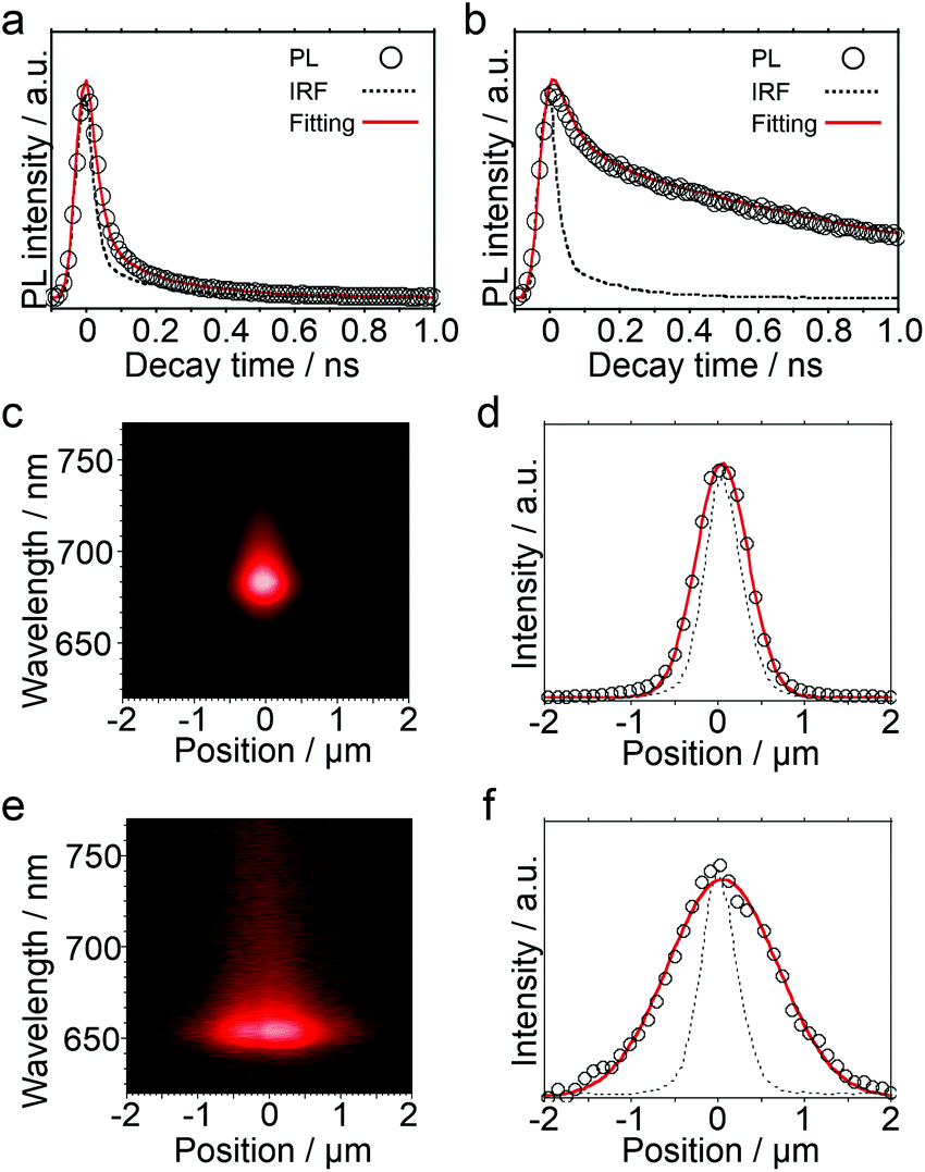 | ||
| Fig. 3 PL decay profiles for the (a) SiO2/Si supported and (b) suspended MoS2 monolayer. The circles indicate the experimental results and the red lines provide the fitted results obtained using a convolution method. Instrument response functions (IRF) are represented by the dotted lines. Wavelength-resolved exciton diffusion PL images and the corresponding PL intensity spatial profiles (circles) of the (c, d) SiO2/Si supported and (e, f) suspended monolayer of MoS2. These profiles were fitted using a Gaussian function (red lines). | ||
| Supported | Suspended | |
|---|---|---|
| τ 1 (ns) | 0.020 | 0.050 |
| τ 2 (ns) | 0.23 | 1.1 |
| C | 0.98 | 0.70 |
| τ eff (ns) | 0.024 | 0.37 |
This suspension technique also allowed observations of PL resulting from interlayer excitons in the MoS2/WS2 vdW heterostructures. Fig. 4 shows the Raman and PL spectra generated by MoS2/WS2 heterostructures grown on a SiO2/Si substrate and suspended on a TEM grid, together with the spectra produced by a specimen grown on hBN. The presence of both MoS2 and WS2 is confirmed by the characteristic Raman vibrational modes in these spectra. The heterostructure produced an E′ + 2LA peak at 356 cm−1 and an A′1 peak at 417.5 cm−1, both attributed to WS2, in addition to E′ and A′1 peaks at 385 and 405 cm−1 attributed to MoS2, as shown in Fig. 4a.33,34 However, the PL spectra obtained from the suspended and SiO2/Si supported samples are profoundly different, as shown in Fig. 4b. Peaks that were initially absent in the range of 1.4–1.7 eV emerge once MoS2/WS2 is removed from the growth substrate. These peaks are assigned to emissions resulting from direct and indirect interlayer excitons, similar to those produced by the heterostructure grown directly on the hBN surface.11 The significant increase in the PL intensity caused by the interlayer excitons in the suspended MoS2/WS2 sample can be readily explained by enhanced interlayer coupling and/or the elimination of substrate-induced non-radiative relaxation.
 | ||
| Fig. 4 (a) Raman and (b) PL spectra obtained from CVD-grown MoS2/WS2 heterostructures supported on a SiO2/Si substrate and suspended in air. The spectra of a MoS2/WS2 heterostructure grown directly on an hBN surface is also shown for comparison. The spectra have been vertically shifted for clarity. | ||
The interlayer coupling was evidently weakened as a result of inhomogeneous modulation in the stacking geometry and the distance between the two layers in the strained heterostructures. This layer-dependent strain was investigated by preparing MoS2/WS2 heterostructures with MoS2 being on top or at the bottom. As shown in Fig. 5, the heterostructures with a bottom MoS2 configuration generated PL peaks derived from the A and B excitons of MoS2 at 1.84 and 1.98 eV, respectively. However, when MoS2 was grown on top, these two peaks were blue-shifted to 1.86 and 2.00 eV. These results suggest a reduction in the tensile strain imparted to the upper MoS2 monolayer in conjunction with the bottom WS2 monolayer, and the significant effect of the growth substrate on coming into contact with the TMDC monolayer. This, in turn, could greatly modify the stacking geometry and the interlayer distance in the vdW heterostructures.
 | ||
| Fig. 5 PL spectra and structure models for (bottom) a MoS2 monolayer grown directly on a SiO2/Si substrate, (center) a WS2 monolayer covered by a MoS2 monolayer, and (upper) a MoS2 monolayer covered by a WS2 monolayer. | ||
It is also noteworthy that suspending the MoS2/WS2 heterostructures enabled an investigation of the relationship between the stacking configuration and the PL derived from the interlayer excitons. Fig. 6 shows HAADF-STEM images of these heterostructures and the corresponding PL spectra obtained at the same regions. The stacking configurations can be determined from a detailed analysis of the STEM images in Fig. 6a–h. Each W and Mo atom evidently overlaps with two S atoms in an adjacent layer, yielding the AA′ stacked heterostructures as shown in Fig. 6a–d, whilst a single W atom is believed to overlap with two S atoms, generating the AB stacked heterostructures as shown in Fig. 6e–h. The results show that, even in the case of an individual grain, the heterostructure may contain different stacking configurations, as shown in Fig. 6a–d, which have also been observed in CVD-grown MoS2 bilayers.35 The PL spectra can be fitted using the Voigt function and the resulting peaks at 1.85 and 2.00 eV are attributed to A and B excitons, respectively, in the MoS2 monolayer, whereas the sharp PL peak at 2.03 eV can be assigned to A excitons in the WS2 monolayer. Interestingly, the peak at 1.63 eV (I3) is only associated with the AA′-stacked region (Fig. 6i). Based on a previous report,11 this I3 peak is assigned to direct interlayer excitons, while the two other peaks (I1, I2) are assigned to indirect excitons. This result indicates that the oscillator strength of the direct interlayer excitons is sensitive to the overlapping wavefunctions of the constituent layers. The detailed analysis of this peak is beyond the scope of the present study and will be reported elsewhere.
 | ||
| Fig. 6 HAADF-STEM images of (a, b) AA′-stacked and (e, f) AB-stacked MoS2/WS2 heterostructures together with their corresponding atomic configuration representations in (c) and (g). Red, blue and yellow spheres indicate Mo, W and S atoms, respectively. Intensity profiles of the selected areas (indicated by white rectangles) in (b) and (f) are shown in (d) and (h). (i) PL spectra (black lines) and fitting curves (red, blue, and gray lines) for suspended AA′- and AB-stacked MoS2/WS2 heterostructures. | ||
Conclusions
In conclusion, this work investigated the effects of the substrate on the optical properties of atomically thin monolayers composed of MoS2 and MoS2/WS2 vdW heterostructures. The present study demonstrates a simple, rapid method for preparing suspended TMDCs and their heterostructures. We observed increases in the PL intensity, lifetime and exciton diffusion length in the case of suspended MoS2 monolayers, and these changes are ascribed to the elimination of substrate-induced non-radiative relaxation. In the case of MoS2/WS2 heterostructures, the restoration of stacking geometry and the enhancement of interlayer coupling enabled observations of interlayer excitons in samples grown on SiO2/Si substrates. Since silicon wafers are one of the most widely used substrates for the growth of TMDC atomic layers, our findings should assist in understanding the intrinsic physical properties of such CVD-grown TMDCs and their heterostructures, thus maximizing their potential for future applications in optoelectronics.Author contributions
K.K. prepared all of the suspended samples and performed the optical analyses. Z.L. carried out the STEM observations. W.Z. conducted time-resolved PL measurements along with Y. Miyauchi and K.M., who provided technical assistance. T.E., T.S., Y.K., K.W., and T.T. prepared samples supported on substrates. Y. Miyata developed the concept and supervised the project. K.K., H.E.L. and Y. Miyata prepared the figures and wrote the paper. All authors discussed the results and commented on the manuscript.Conflicts of interest
There are no conflicts to declare.Acknowledgements
This work was supported by the JST CREST (grant no. JPMJCR16F3), the “ZE Research Program, IAE ZE30B-10”, and the JSPS KAKENHI Grant Numbers JP18H01832, JP17K19055, JP16H06331.References
- M. Chhowalla, H. S. Shin, G. Eda, L.-J. Li, K. P. Loh and H. Zhang, Nat. Chem., 2013, 5, 263 CrossRef PubMed.
- K. F. Mak and J. Shan, Nat. Photonics, 2016, 10, 216 CrossRef CAS.
- Q. H. Wang, K. Kalantar-Zadeh, A. Kis, J. N. Coleman and M. S. Strano, Nat. Nanotechnol., 2012, 7, 699 CrossRef CAS PubMed.
- J. He, D. He, Y. Wang, Q. Cui, F. Ceballos and H. Zhao, Nanoscale, 2015, 7, 9526–9531 RSC.
- Q. Cui, F. Ceballos, N. Kumar and H. Zhao, ACS Nano, 2014, 8, 2970–2976 CrossRef CAS PubMed.
- H. Fang, C. Battaglia, C. Carraro, S. Nemsak, B. Ozdol, J. S. Kang, H. A. Bechtel, S. B. Desai, F. Kronast, A. A. Unal, G. Conti, C. Conlon, G. K. Palsson, M. C. Martin, A. M. Minor, C. S. Fadley, E. Yablonovitch, R. Maboudian and A. Javey, Proc. Natl. Acad. Sci. U. S. A., 2014, 111, 6198–6202 CrossRef CAS PubMed.
- P. Rivera, K. L. Seyler, H. Yu, J. R. Schaibley, J. Yan, D. G. Mandrus, W. Yao and X. Xu, Science, 2016, 351, 688–691 CrossRef CAS PubMed.
- H. Chen, X. Wen, J. Zhang, T. Wu, Y. Gong, X. Zhang, J. Yuan, C. Yi, J. Lou, P. M. Ajayan, W. Zhuang, G. Zhang and J. Zheng, Nat. Commun., 2016, 7, 12512 CrossRef CAS PubMed.
- J. Kim, C. Jin, B. Chen, H. Cai, T. Zhao, P. Lee, S. Kahn, K. Watanabe, T. Taniguchi, S. Tongay, M. F. Crommie and F. Wang, Sci. Adv., 2017, 3, e1700518 CrossRef PubMed.
- D. Unuchek, A. Ciarrocchi, A. Avsar, K. Watanabe, T. Taniguchi and A. Kis, Nature, 2018, 560, 340–344 CrossRef CAS PubMed.
- M. Okada, A. Kutana, Y. Kureishi, Y. Kobayashi, Y. Saito, T. Saito, K. Watanabe, T. Taniguchi, S. Gupta, Y. Miyata, B. I. Yakobson, H. Shinohara and R. Kitaura, ACS Nano, 2018, 12, 2498–2505 CrossRef CAS PubMed.
- B. Miller, A. Steinhoff, B. Pano, J. Klein, F. Jahnke, A. Holleitner and U. Wurstbauer, Nano Lett., 2017, 17, 5229–5237 CrossRef CAS PubMed.
- D. Kozawa, A. Carvalho, I. Verzhbitskiy, F. Giustiniano, Y. Miyauchi, S. Mouri, A. H. Castro Neto, K. Matsuda and G. Eda, Nano Lett., 2016, 16, 4087–4093 CrossRef CAS PubMed.
- T. Yamaoka, H. E. Lim, S. Koirala, X. Wang, K. Shinokita, M. Maruyama, S. Okada, Y. Miyauchi and K. Matsuda, Adv. Funct. Mater., 2018, 28, 1801021 CrossRef.
- N. Lu, H. Guo, L. Wang, X. Wu and X. C. Zeng, Nanoscale, 2014, 6, 4566–4571 RSC.
- W. Yang, H. Kawai, M. Bosman, B. Tang, J. Chai, W. L. Tay, J. Yang, H. L. Seng, H. Zhu, H. Gong, H. Liu, K. E. J. Goh, S. Wang and D. Chi, Nanoscale, 2018, 10, 22927–22936 RSC.
- M. R. Habib, H. Li, Y. Kong, T. Liang, S. M. Obaidulla, S. Xie, S. Wang, X. Ma, H. Su and M. Xu, Nanoscale, 2018, 10, 16107–16115 RSC.
- K. Wang, B. Huang, M. Tian, F. Ceballos, M.-W. Lin, M. Mahjouri-Samani, A. Boulesbaa, A. A. Puretzky, C. M. Rouleau, M. Yoon, H. Zhao, K. Xiao, G. Duscher and D. B. Geohegan, ACS Nano, 2016, 10, 6612–6622 CrossRef CAS PubMed.
- Y. Li, Q. Cui, F. Ceballos, S. D. Lane, Z. Qi and H. Zhao, Nano Lett., 2017, 17, 6661–6666 CrossRef CAS PubMed.
- M. Z. Bellus, F. Ceballos, H.-Y. Chiu and H. Zhao, ACS Nano, 2015, 9, 6459–6464 CrossRef CAS PubMed.
- K. Kang, S. Xie, L. Huang, Y. Han, P. Y. Huang, K. F. Mak, C.-J. Kim, D. Muller and J. Park, Nature, 2015, 520, 656 CrossRef CAS PubMed.
- S. Li, S. Wang, D.-M. Tang, W. Zhao, H. Xu, L. Chu, Y. Bando, D. Golberg and G. Eda, Mater. Today, 2015, 1, 60–66 CrossRef.
- A. M. van der Zande, P. Y. Huang, D. A. Chenet, T. C. Berkelbach, Y. You, G.-H. Lee, T. F. Heinz, D. R. Reichman, D. A. Muller and J. C. Hone, Nat. Mater., 2013, 12, 554 CrossRef CAS PubMed.
- M. Okada, T. Sawazaki, K. Watanabe, T. Taniguch, H. Hibino, H. Shinohara and R. Kitaura, ACS Nano, 2014, 8, 8273–8277 CrossRef CAS PubMed.
- Y. Kobayashi, S. Sasaki, S. Mori, H. Hibino, Z. Liu, K. Watanabe, T. Taniguchi, K. Suenaga, Y. Maniwa and Y. Miyata, ACS Nano, 2015, 9, 4056–4063 CrossRef CAS PubMed.
- H. Shi, R. Yan, S. Bertolazzi, J. Brivio, B. Gao, A. Kis, D. Jena, H. G. Xing and L. Huang, ACS Nano, 2013, 7, 1072–1080 CrossRef CAS PubMed.
- T. Kato and T. Kaneko, ACS Nano, 2016, 10, 9687–9694 CrossRef CAS PubMed.
- Y. Huang, E. Sutter, L. M. Wu, H. Xu, L. Bao, H.-J. Gao, X.-J. Zhou and P. Sutter, ACS Appl. Mater. Interfaces, 2018, 10, 23198–23207 CrossRef CAS PubMed.
- Y. Lin, X. Ling, L. Yu, S. Huang, A. L. Hsu, Y.-H. Lee, J. Kong, M. S. Dresselhaus and T. Palacios, Nano Lett., 2014, 14, 5569–5576 CrossRef CAS PubMed.
- A. Raja, A. Chaves, J. Yu, G. Arefe, H. M. Hill, A. F. Rigosi, T. C. Berkelbach, P. Nagler, C. Schüller, T. Korn, C. Nuckolls, J. Hone, L. E. Brus, T. F. Heinz, D. R. Reichman and A. Chernikov, Nat. Commun., 2017, 8, 15251 CrossRef PubMed.
- S. Mouri, Y. Miyauchi, M. Toh, W. Zhao, G. Eda and K. Matsuda, Phys. Rev. B: Condens. Matter Mater. Phys., 2014, 90, 155449 CrossRef.
- L. Yuan, T. Wang, T. Zhu, M. Zhou and L. Huang, J. Phys. Chem. Lett., 2017, 8, 3371–3379 CrossRef CAS PubMed.
- C. Lee, H. Yan, L. E. Brus, T. F. Heinz, J. Hone and S. Ryu, ACS Nano, 2010, 4, 2695–2700 CrossRef CAS PubMed.
- A. Berkdemir, H. R. Gutiérrez, A. R. Botello-Méndez, N. Perea-López, A. L. Elías, C.-I. Chia, B. Wang, V. H. Crespi, F. López-Urías, J.-C. Charlier, H. Terrones and M. Terrones, Sci. Rep., 2013, 3, 1755 CrossRef.
- M. Xia, B. Li, K. Yin, G. Capellini, G. Niu, Y. Gong, W. Zhou, P. M. Ajayan and Y.-H. Xie, ACS Nano, 2015, 9, 12246–12254 CrossRef CAS PubMed.
| This journal is © The Royal Society of Chemistry 2019 |