
 Open Access Article
 This Open Access Article is licensed under a Creative Commons Attribution-Non Commercial 3.0 Unported Licence
Evolution of local conductance pathways in a single-molecule junction studied using the three-dimensional dynamic probe method†
Atsushi
Taninaka
,
Shoji
Yoshida
,
Yoshihiro
Sugita
,
Osamu
Takeuchi
and
Hidemi
Shigekawa
 *
*
Faculty of Pure and Applied Sciences, University of Tsukuba, Tsukuba 305-8571, Japan. E-mail: hidemi@ims.tsukuba.ac.jp
First published on 7th March 2019
Abstract
Understanding of the dynamics of the bonding states of molecules with electrodes while the molecular conformation is changed is particularly important for elucidating the details of electrochemical devices as well as molecular devices in which the reaction dynamics of the electrodes and molecules plays an important role, such as in fuel cells, catalysis and bioelectrochemical devices. However, it has been difficult to make measurements when the distance between counter electrodes is short, namely, the molecule is raised from a lying form, almost parallel and close to the electrodes, toward a standing form and vice versa. We previously have developed a method called the three-dimensional (3D) dynamic probe method, which enables conductance measurement while the conformation of a single-molecule junction is precisely controlled by scanning tunneling microscopy (STM) techniques. Here, by combining this method with density functional theory (DFT) calculations, it has become possible to simultaneously consider the effects of the dynamics of molecular structures and the bonding states at the electrodes on the local transmission pathways, local-bond contributions to conductance. Here, by performing an analysis on 1,4-benzenediamine (BDA) and 1,4-benzenedithiol (BDT) single molecule junctions, we have observed, for the first time, the effect of a change in the molecular conformations and bonding states on the local transmission pathways for a short Au electrode distance condition.
Introduction
In the design of nanoscale electronic devices making full use of single molecule characteristics, it is essential to elucidate the relationship between the conformations of single molecules and the conduction properties. Furthermore, understanding of the dynamics of the bonding states of molecules with electrodes while the molecular conformation is changed is particularly important for elucidating the details of electrochemical devices as well as molecular devices in which the reaction dynamics of the electrodes and molecules plays an important role, such as in fuel cells, catalysis and bioelectrochemical devices.1–4Such conduction properties of single molecules have been studied for various molecules by the break junction (BJ) method, and valuable results have been obtained.5–17 However, in the BJ method, since the electrodes are connected and ruptured in each measurement, the junction structure is unknown and it is difficult to analyze whether the change in the measured conductance corresponds to the change in the conduction path due to the change in the contact structure or to the change in the transmittance due to the change in the molecular conformation.
Recently, a method that enables conductance measurement while changing the angle of the molecule to the substrate without destroying the junction has been developed as a type of BJ method;6,11,17 however, it is still difficult to analyze the structure of the bonding states. Since the dynamics of the contact point between the molecule and substrate affects the scattering of electrons when electrons are injected, it is necessary to simultaneously elucidate the conduction characteristics and the structures of the bonding states.
We previously developed a method called the three-dimensional (3D) dynamic probe method, which enables conductance measurement while the conformation of a single-molecule junction is precisely controlled by scanning tunneling microscopy (STM) techniques.18–21 By combining this method with density functional theory (DFT) calculations, it has become possible to simultaneously consider the effects of the dynamics of molecular structures and the bonding states at the electrodes on the local transmission pathways and conductance.18–20,22–24
However, the measurements in the previous studies were carried out with a gold STM tip sufficiently retracted from the substrate surface, namely molecules were in a standing form and thus formed junctions with the electrodes only at their two ends. When a molecule is in a lying form, almost parallel and close to the electrodes, the interaction between the molecule and the substrate is considered to be stronger, and conduction pathways are considered to exist between the electrodes via various parts of the molecule instead of a single flow through the molecule. As the molecule is raised, such direct conduction pathways between the electrodes begin to break and the bonding state changes into structures where junctions are formed only at the two ends of the molecule and an influence of the structure peculiar to each molecule appears. Although it is very important to understand the conductance properties appearing in such a dynamic change, as described above, they have not yet been investigated.
To clarify the change in the bonding states while the molecular conformation is varied from a lying to standing conformation and vice versa, we carried out 3D dynamic probe experiments and DFT simulations on 1,4-benzenediamine (BDA) and 1,4-benzenedithiol (BDT) molecules for comparison. BDA and BDT are compounds having one benzene ring. BDA is not connected to Au adatoms on the substrate but its lone pair forms a bond, which is expected to attract the molecule to the substrate and prevent the rotation of the molecule.19 In contrast, BDT, one of the simplest molecules which has often been used for BJ analysis,5,6,8–10,20 forms bonds with the Au adatoms on both electrodes, which allows rotational motion during a conformational change.20 Understanding of such differences is important for elucidating the details of electrochemical devices as well as molecular devices in which the reaction dynamics of the electrodes and molecules plays an important role, such as in fuel cells, catalytic actions and bioelectrochemical devices.1–4
Experimental
Sample and tip preparation
A clean flat Au(111) surface was prepared by evaporating Au of 100 nm thickness on a mica substrate that had been subjected to Ar sputtering (5 min, 1 μA cm−2) and annealing (30 min, 700 K) for 3–5 cycles. Then the Au(111) surface was exposed to BDA or BDT molecules introduced through a variable leak valve (10 s, partial pressure: 1.0 × 10⁻⁶ Pa). The STM tip was formed by cutting a Au wire (0.3 mm diameter). All measurements were carried out under vacuum (<5.0 × 10⁻⁸ Pa) using an Omicron LT STM system. By cooling the STM unit with liquid nitrogen for over one week, the temperature in the STM chamber was maintained at 83 K and the thermal drift was reduced.Experimental scheme and measurements
Fig. 1a and b show the schematics of the molecular structures of BDA and BDT deposited on a Au(111) surface, respectively.25,26 In BDA, the N atoms connected to the surface side and the probe (STM tip) side are denoted by NS and Nt, respectively. On the other hand, BDT adsorbs with a Au adatom bound to thiol groups at both ends.20 For convenience, we denote the Au atoms on the substrate side and probe (tip) side as Auads and Auadt, respectively, and the S atoms bonded to Auads and Auadt atoms are indicated by the slightly smaller red circles and named SS and St, respectively. Fig. 1c and d show STM images obtained after the deposition of BDA and BDT molecules on a Au (111) surface, respectively. Similar to that in previous papers,19,20 it was confirmed that single BDT and BDA molecules were adsorbed at the elbow sites of the herringbone structure of the Au (111) surface, as shown by yellow arrows. | ||
| Fig. 1 Measurement setup. (a, b) Schematics of the molecular structures of BDA and BDT deposited on a Au(111) surface, respectively. (c, d) STM images of BDA and BDT molecules on a Au (111) surface, respectively. (e) Schematic of the 3D dynamic probe method. (f) Schematic of the measurement scheme. | ||
After observing a target BDA or BDT molecule (VS = 0.2 V, I = +0.2 nA), the STM tip was moved above it. When the molecule was picked up, a rapid increase in conductance was observed. Since the molecular junction was unstable above the herringbone structure, we moved the junction away from the structure for measurement. Then the feedback was turned off and the sample bias voltage VS was decreased to 10 mV because the bond was unstable at high bias voltages. Then, the STM tip was moved back and forth in the Z-direction in accordance with a sinusoidal function (zp–p = 0.224 nm, 50 Hz), and was made to slowly approach the target molecule. The formation of a junction was confirmed by a rapid increase in current. After the formation was confirmed, the STM tip was moved back slightly (0.14 nm) to ensure a stable measurement, and a two-dimensional scan was carried out step by step after each cycle of Z-modulation (X, Y, Z: 56 × 36 × 200 and 40 × 40 × 200 points in the case of Fig. 2a and b, respectively) over the molecule, as shown in Fig. 1e. Fig. 1f shows the measurement scheme and an example of the obtained data and their magnifications. The blue, orange, green, and red lines indicate X- and Y-scans, the Z-modulation, and the normalized conductance G/G0, respectively (G0 = 2e2/h, h is Planck's constant). By plotting the value of G/G0 obtained at the STM tip position (X, Y, Z), a 3D volume plot can be obtained, as shown in Fig. 2a and b. This shows the change in conductance with the conformational change of the single molecule junction. The effect of the sample gradient was removed by linear correction.
 | ||
| Fig. 2 3D plot and the analysis method. (a, b) 3D plots obtained for BDA and BDT molecules, respectively. (c) Schematic diagram to determine the adsorption angle. φ represents the angle between the molecule and the substrate considering the direction of the molecule (see Fig. S1† for details). (d, e) YZ cross sections for the cases of BDA and BDT, respectively. | ||
Results and discussion
Experimental results
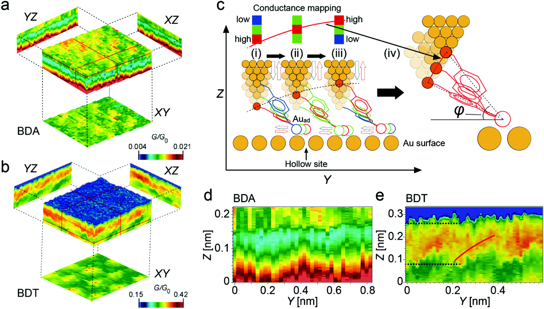
Fig. 2a and b show 3D plots obtained for BDA and BDT molecules, respectively. The high-conductance regions in the XY cross sections have the same periodicity as the Au(111) atomic structure. Therefore, it is considered that the Auads and the NS moved reproducibly on the Au(111) surface during measurement, which reflects the change in conductance with the position of the Auads and the NS on the Au(111) surface, as was observed in our previous studies.19,20 From the high reproducibility of the 3D patterns, the bond structure at the STM tip apex is considered to have been stable during the measurement, showing the single-molecule level analysis reliable.This measurement method allows the adsorption angle of a molecule (φ in Fig. 2c) to be obtained from the XZ and YZ cross sections of the conductance map, and the location of the junction point can be obtained from the XY cross section.19,20Fig. 2c shows a schematic diagram showing the relationship between the YZ cross section of the conductance map and the adsorption angle of the molecule in the case of BDT. During the conformational change of BDT induced by Z-modulation, the location of Auads moves. When Auads is on hollow and on-top sites, the conductance is large and small, respectively. The motion of the molecule induced by Z-modulation is schematically shown in Fig. 2c for the movement of Auads (i) from a hollow site to an on-top site, (ii) from a bridge site to another bridge site via a hollow site, and (iii) from an on-top site to a hollow site.
The conduction depends on the adsorption position of Auads as shown in the color bars in the upper part of each figure in Fig. 2c. When the probe moves in the X- or Y-direction, the relationship between the height of the probe and the adsorption position of Auads changes. For example, if the pulling of the molecule starts from a (ii) bridge site and (iii) an on-top site, the probe height when Auads reaches the hollow site changes, resulting in a change in the red squares in the color bars. That is, the Z position at which the conductance becomes large follows that of the upper end of a BDT molecule whose lower end is on a hollow site. Namely, the red line drawn over the color bars corresponds to the trajectory of the upper Auadt when an arc of the molecular length is drawn with the lower-end Auads placed on a hollow site, as shown in Fig. 2c(iv). Thus, the adsorption angle of the molecule can be derived from the analysis of the arc pattern shown in the YZ and XZ cross sections, as was carried out in previous studies.19,20
Fig. 2d and e show the YZ cross sections for the cases of BDA and BDT, respectively. In previous experiments, the results were obtained for a region where the probe–substrate distance was larger than 0.58 nm for BDA and larger than 0.74 nm for BDT. Thus, the initial Z distance is shorter in each case in this experiment than in the previous experiments. In the case of BDA, there was no arc-like change in the conductance map (Fig. 2d). This is considered to be due to the BDA molecule not being bound to Auads and Auadt and it being almost parallel and closer to the surface in the lying conformation. This allowed conduction pathways to form between the functional groups other than the amino groups, such as benzene rings, and the substrate surface; thus, no site-dependent change in the conductance was observed.
In contrast, in the case of BDT, a bright region was observed in the Z-range of 0.08–0.26 nm, which is considered to be due to the Auads and Auadt bound to the end of the BDT, meaning that the number of conductive pathways was limited compared with that in the case of BDA, and a change in the conductance map was observed. However, the Z-region with high conductance is wide, which indicates that Auads does not move from a hollow site during the Z-modulation of ∼ 0.15 nm (Fig. 2e). Taking into account the angle of the molecule in the XY plane and assuming that BDT is parallel to the substrate at Z = 0, the angle becomes 20° and 26° at Z = 0.1 and 0.2 nm, respectively (see Fig. S1† and its caption for details).
Fig. 3a and b show two typical conductance curves, namely, the normalized conductance G/G0 as a function of the probe–substrate distance for retract and approach motion, obtained for a BDA molecule at positions A and B in Fig. 3c(i). Unlike the results in the previous paper,19 where the distance between the probe and the substrate was sufficiently large, no hysteresis appeared and the conductance curves obtained for the retract and approach motion were almost the same. According to the previous results, the hysteresis of the conductance in BDA was found to be due to the difference in the timing of the formation of the bond between the lone pair and the on-top site in the retract and approach motion. Therefore, when the probe–substrate distance was short, as in this case, such a change in the timing did not occur while Z was changed in this range.
 | ||
| Fig. 3 Data obtained for BDA. (a, b) Two typical conductance curves of a BDA molecule obtained by the retract and approach motion at positions A and B in (c) (i). (c) XY conductance maps corresponding to the Z-positions (I) to (V) in (a). | ||
The difference between the conductance curve in Fig. 3a and b is the change observed from (IV) to (V); the conductance became large and then gradually decreased as shown in Fig. 3a, while it continued to gradually increase as shown in Fig. 3b. This difference is considered to be because of the change in the bonding state between the lone pair of NS and the Auads atom while the BDA molecule being pulled up and down is not large. Namely, instead of the binding site moving between two adjacent on-top sites, it is considered to move from an on-top site to a bridge site, which does not produce hysteresis.
Fig. 3c shows the XY conductance maps corresponding to the Z-positions (I) to (V) shown in Fig. 3a. The structure of the Au(111) surface was not observed in Fig. 3c(I), but it started to appear in (III), where the details are shown in the images in the lower row ((III)-1 to (III)-3). This is considered to be due to the fact that BDA stood from the surface and the functional group forming the transmission pathway with the on-top site became only the amino group on the surface side. The atomic pattern of Au was shifted upward by about 0.1 nm in the Y direction, as indicated by the broken line in Fig. 3c(III) and (IV). Since this is less than the distance between two on-top sites, the shift is considered to be due to the movement of the Auad from an on-top site to a bridge site, as described above.
Fig. 4a and b show the conductance curves of BDT and the XY conductance maps obtained at different probe–substrate distances ((I) to (VIII) in Fig. 4a), respectively. The location where the conductance became large in Fig. 4b was determined in a previous work to be the hollow site on the Au(111) surface.20 As shown in Fig. 4a, similar to the case of BDA, the conductance curves in the retract and approach motion did not show any hysteresis and were almost identical, unlike the results in the previous work in which the probe–substrate distance was sufficiently large.20 Although there is a Auads in the case of BDT, when the distance between the probe and the substrate is short, it is considered that the BDT molecule and Auads do not move significantly on the surface. Namely, this change is considered to be due to the fact that Auads moved between a bridge site and a hollow site via the same pathway for the retract and approach motion instead of between two adjacent hollow sites.
 | ||
| Fig. 4 Data obtained for BDT. (a) Typical conductance curves of a BDT molecule obtained by the retract and approach motion. (b) XY conductance map corresponding to the Z-positions (I) to (VIII) in (a). | ||
As shown in Fig. 4b, the conductance map closely reflects the atomic structure of the Au(111) surface, in contrast to the case of BDA. From (I) to (IV), the contrast gradually changed and, as shown by the broken line in Fig. 4b, the location where the conductance was large was shifted by about 0.13 nm (half of the Au atomic radius), which supports the hypothesis that Auads moved between a bridge site and a hollow site via the same pathway for the retract and approach motion. From (IV) to (VII), G/G0 gradually decreased, and although the contrast changed, the location with high conductance did not show any shifts in Fig. 4b. Then G/G0 rapidly decreased from ∼0.30 to ∼0.15 from (VII) to (VII)′. Since the conductance was rapidly halved, it is considered that the number of transmission pathways was halved.
Simulations
To understand the experimental results in detail, we carried out simulations for BDA and BDT molecules. We used Atomistix ToolKit software (version 12.8.2 Quantum Wise A/S), with DFT within the local density approximation (LDA) using the Perdew–Zunger (PZ) exchange–correlation function27 to simulate the optimized structures of the junction and the variation in its conductance while the STM tip was retracted. A double-ζ basis set was used for all atomic species and the cutoff energy was set to 100 Ry. The sampling for Brillouin zone integration was performed at 3 × 3 × 400 k-points. The conductance was calculated by the non-equilibrium Green's function (NEGF) method.28,29 A bias voltage of 10 mV was applied to the electrodes, and three layers of Au(111) were prepared. Although DFT underestimates the energy gap, which may result in a larger conductance, the relative change in conductance is reliable.12,30,31A Au atom (adatom) was added to a hollow site on the Au(111) surface on the upper electrode as the STM tip apex. Structural optimization was first carried out only with a molecule, where BDA was in the cis conformation. The molecular surface was made parallel to the substrate and, as shown in Fig. 1a, it was placed so that both ends were on on-top sites. This condition was used for the calculation for comparison with the experimental result shown in Fig. 3a. Next, when the electrode on the probe side was brought closer, coupling occurred at a certain distance. The height of the upper-electrode-side N atom from the Au(111) substrate surface (lower side) was 0.21 nm lower than the initial height in the previous work (0.58 nm).19 First, optimization was performed in this state once. Then the molecule was pulled up step by step (0.3 nm for each step) and optimization was carried out again between each step, where the local pathway and G were obtained. In the calculation for comparison with the experimental result shown in Fig. 3b, the molecule was moved along the <110> direction as the NS atom was located on a bridge site. Then a similar procedure to that described above was carried out.
For the BDT molecule, similar optimizations were carried out but with the Au adatoms Auadt and Auads at both ends of the molecule, which were placed at hollow sites in accordance with the structure shown in Fig. 1b. After the first structural optimization and the calculation of the conductance, the distance between the two electrodes was changed in steps of 0.02 nm up to 0.34 nm. The upper-electrode-side Au adatom (Auadt) was fixed during the whole process to reflect the stable junction structure at the STM tip apex because highly reproducible conductance patterns were obtained in measurements. Since more detailed analysis is necessary for the calculations while the STM tip is made to approach the substrate, simulations were carried out for the case of STM tip retraction here.
First we discuss the case of BDA. Fig. 5a shows a conductance curve obtained for BTA, which is in good agreement with the experimental result shown in Fig. 3a. Fig. 5b shows the conformations and local transmission contributions obtained for (i) to (v) in Fig. 5a, which correspond to the change from (I) to (V) in Fig. 3a. Structural optimization was first carried out only with a free molecule, where BDA has a cis conformation. The molecular surface was set parallel to the substrate and it was placed so that both ends were on the on-top sites as shown in Fig. 1a. Then, as the electrode on the probe side was brought closer, coupling occurred at a certain distance. Optimization was first performed in this state. Then the molecule was pulled up step by step (0.03 nm for each step) and optimization was carried out between each step, where the local pathway and G were obtained. Fig. 5b(i) shows the optimized conformation after one step.
 | ||
| Fig. 5 Simulated conductance curve obtained for BDA. (a) Simulated conductance curve corresponding to the change from (I) to (V) in Fig. 3a. (b) Schematics of conformational structures and local transmission contributions for (i) to (v) in (a). Local transmission contributions are proportional to the thickness of the arrows. | ||
In contrast to the previous work,19 the site of the bond did not change significantly while the distance between two electrodes was short. In (i), several transmission pathways were formed around the functional groups other than the amines of BDA, such as the benzene ring and current flowed from some other sites on the substrate, rather than an electron flow through the benzene ring of BDA. The existence of several local transmission pathways is considered to be the reason for the low contrast of the atomic structures shown in Fig. 3c. In (iii), the contribution of Au/Nt/Au to the local transmission decreases and the contribution of the local transmission near the Ns atom becomes large, which is considered to have made the atomic structure in Fig. 3c clearer.
In Fig. 5b(i)–(iii), the position of the Ns atom slightly moves from the on-top site, strengthening the transmission pathway formed by the coordination bond15 between the lone pair of NS and AuN. However, as the distance between Nt and the substrate increases, its transmission decreases, resulting in the observed decrease in G/G0 from (i) to (iii). In (iii), NS is above AuN and forms a transmission pathway via the coordination bond19 between the lone pair of NS and AuN. At this time, since CN is not above AuC, its contribution is small, and the conductance between NS and AuN can be observed in the conductance map. In (iv), since CN moves above AuC, forming two transmission pathways of NS–AuN and CN–AuC, the conductance becomes large. In (v), CN is pulled away from the substrate and the contribution of the conduction between CN and AuC to the transmission becomes small. These changes closely reproduce the observed result. From the positions of the NS atom between Fig. 5b(iii) and (iv), the displacement of the NS atom was estimated to be 0.11 nm, which is in agreement with the displacement in the conductance map in Fig. 3c (0.1 nm).
To reproduce the conductance curve in Fig. 3b, the initial structure was changed and calculations were carried out. The initial position of the molecular end was moved away from the on-top site. Namely, the bond structure between Auad and Nt, and the position of NS were changed.
Although calculations were carried out for various distances moved, almost the same results were obtained. Fig. 6a and b show the calculated conductance curve and the schematic structures corresponding to (i) to (v) in Fig. 6a, respectively. The conductance curve was in good agreement with the experimental curve shown in Fig. 3b.
 | ||
| Fig. 6 Simulated conductance curve obtained for BDA. (a) Simulated conductance curve corresponding to the change from (I) to (V) in Fig. 4b. (b) Schematics of conformational structures and local transmission contributions for (i) to (v) in (a). Local transmission contributions are proportional to the thickness of the arrows. | ||
The positional relationship between Auad and Nt was fixed similarly to that in a previous work20 so that the relative position between the upper electrode as the probe and Nt did not change while raising the BDA molecule. The calculated contributions of the local transmission22–24 between Auad and Nt shown in Fig. 6b gradually decreased from (iii) to (v) (3.1 × 10⁻², 2.7 × 10⁻², and 2.4 × 10⁻², respectively), differing from the observed change shown in Fig. 6a, which is due to the increase in the angle between Nt and the BDA molecular plane. In addition, although NS moves from an on-top site to a bridge site from (i) to (v) in Fig. 5b, NS is at a bridge site with low conductivity for (i) to (iii) and moves to an on-top site with high conductivity in Fig. 6b. Actually, the calculated contribution of the local transmission between NS and AuN increased from (i) to (iii) (7.9 × 10⁻³, 8.4 × 10⁻³, and 1.2 × 10⁻², respectively), resulting in an increase in the total conductance, which is in good agreement with the observed change from (iii) to (v) shown in Fig. 6a.
Although it was difficult to directly evaluate the adsorption energy because of the existence of the STM tip which pulled up the molecule, the interaction between the BDA lone pair and Au atom was dominant even in the lying form in (i) and (ii). The binding between CN and AuC was weaker than that via the lone pair. As the conformation changed into the standing form as (iii) to (v), the binding became to be a single interaction. The structure maintained for a further pulling position as shown in a previous paper,19 which is in good agreement with the idea that relatively sharp conductance histogram peaks were observed for the amine–Au system due to the relatively weak gold–amine interaction, namely, amines can only significantly bind to gold adatoms in a standing form.12
As has been shown, the dynamics of the bond state in the BDA single-molecule junction for a small probe–substrate distance was well explained by the results obtained by combining the 3D dynamic probe method and DFT calculations. A similar simulation was then carried out for the BDT molecule. Fig. 7a shows the conductance curve obtained by the simulation. The change in conductance from (i) to (iv) is in good agreement with the observed change shown in Fig. 4a. However, the calculated conductance rapidly decreases between (iv) and (vi) and gradually decreases from (vi) to (viii), while in the experiments, it rapidly decreased after a gradual decay.
 | ||
| Fig. 7 Simulated conductance curve obtained for BDT. (a) Simulated conductance curve corresponding to the change in Fig. 4a. (b) Schematics of conformational structures and local transmission contributions for (i) to (viii) in (a). The direction of the arrows from the upper substrate to SS shown in (vii) and (viii) indicates the negative contribution. Local transmission contributions are proportional to the thickness of the arrows. | ||
Fig. 7b shows the conformations used for the calculations and the obtained contributions to the local transmission. Similar simulation procedures to those discussed earlier were carried out (see Experimental for the initial conditions). From (i) to (iv), because the contributions to the local transmission via the Auadt-St-substrate (upper side) and Auads-SS-substrate (lower side) are larger than that via the phenyl group (benzene ring) of the BDT transmission pathway, there is not a single transmission pathway passing through the BDT molecule, and these are two dominant pathways at both ends of the molecule shown by the pink arrows.
In the change from (iv) to (vi), the local transmission contributions of these two pathways become smaller and one of them disappears. The calculated values of G/G0 for (iv) and (v)′ were 1.11 and 0.53, respectively, in good agreement with the decrease to the values shown in Fig. 4a (VII) and (VII)′. This rapid change in conductance is due to the rotation of the benzene ring of BDT as shown in Fig. 7. Then the local transmission contribution via the phenyl group (benzene ring) becomes dominant, as shown by the light green arrow in (viii), which decreases with the increase in Z, producing the gradual decrease in the conductance shown in Fig. 7a.
In the experiment, a gradual decrease in conductance was observed from (IV) to (VII) before the rapid change from (VII) to (VIII) as shown in Fig. 4a. This is considered to be because the rotation of BDT begins after the two Au/S/Au pathways become one in the simulation, while the rotation occurred first in the experiment. This difference is considered to be due to the actual tip surface not being flat similarly to the substrate used for the calculation, but having a pyramidal structure, which reduces the effect of steric hindrance in the calculation.
To see the conformational change in the molecule in more detail, Fig. 8 shows the conformations shown in Fig. 7b as seen from the Z-direction. Auads moves from a hollow site to a bridge site. The distance moved is 0.15 nm, as shown by the broken line, which is in good agreement with the value of 0.13 nm experimentally obtained for the change from (I) to (IV) as shown in Fig. 4b. Auads does not move from (vi) to (viii) while the molecule is pulled up, as shown by the broken line, which is considered to be due to the rotation of the molecule during the change in Z.
 | ||
| Fig. 8 Schematic structures of BDA on a Au(111) surface. Conformations of BDA shown in Fig. 7b as seen from the Z-direction. | ||
Conclusions
By performing analysis on 1,4-benzenediamine (BDA) and 1,4-benzenedithiol (BDT) single molecule junctions by the 3D dynamic probe method and DFT calculations, we have observed, for the first time, the effect of a change in the molecular conformations and bonding states on the local transmission pathways for a short Au electrode distance. The obtained results are expected to play an important role in advancing the development of nanoscale devices making full use of the characteristics of single molecules.Conflicts of interest
There are no conflicts to declare.Acknowledgements
H.S. and S.Y. acknowledge the financial support from the Japan Society for the Promotion of Science, the Grant-in-Aid for Scientific Research 17H06088, and the Grant-in-Aid for Young Scientists (A) 16H05982, respectively.Notes and references
- D. Kahanda, K. T. DuPrez, E. Hilario, M. A. McWilliams, C. H. Wohlgamuth, L. Fan and J. D. Slinker, Anal. Chem., 2018, 90, 2178–2185 CrossRef CAS.
- Y. van de Burgt, E. Lubberman, E. J. Fuller, S. T. Keene, G. C. Faria, S. Agarwal, M. J. Marinella, A. Alec Talin and A. Salleo, Nat. Mater., 2017, 16, 414 CrossRef CAS.
- C. Santoro, C. Arbizzani, B. Erable and I. Ieropoulos, J. Power Sources, 2017, 356, 225–244 CrossRef CAS.
- A. J. Bandodkar, C. S. López, A. M. Vinu Mohan, L. Yin, R. Kumar and J. Wang, Sci. Adv., 2016, 2, e1601465 CrossRef.
- S. V. Aradhya and L. Venkataraman, Nat. Nanotechnol., 2013, 8, 399 CrossRef CAS.
- C. Bruot, J. Hihath and N. Tao, Nat. Nanotechnol., 2011, 7, 35 CrossRef.
- M. S. Hybertsen and L. Venkataraman, Acc. Chem. Res., 2016, 49, 452–460 CrossRef CAS.
- S. Kaneko, D. Murai, S. Marqués-González, H. Nakamura, Y. Komoto, S. Fujii, T. Nishino, K. Ikeda, K. Tsukagoshi and M. Kiguchi, J. Am. Chem. Soc., 2016, 138, 1294–1300 CrossRef CAS.
- M. Kiguchi, H. Nakamura, Y. Takahashi, T. Takahashi and T. Ohto, J. Phys. Chem. C, 2010, 114, 22254–22261 CrossRef CAS.
- Y. Komoto, S. Fujii, H. Nakamura, T. Tada, T. Nishino and M. Kiguchi, Sci. Rep., 2016, 6, 26606 CrossRef CAS.
- S. Y. Quek, M. Kamenetska, M. L. Steigerwald, H. J. Choi, S. G. Louie, M. S. Hybertsen, J. B. Neaton and L. Venkataraman, Nat. Nanotechnol., 2009, 4, 230 CrossRef CAS.
- S. Y. Quek, L. Venkataraman, H. J. Choi, S. G. Louie, M. S. Hybertsen and J. B. Neaton, Nano Lett., 2007, 7, 3477–3482 CrossRef CAS.
- H. Vazquez, R. Skouta, S. Schneebeli, M. Kamenetska, R. Breslow, L. Venkataraman and M. S. Hybertsen, Nat. Nanotechnol., 2012, 7, 663 CrossRef CAS.
- L. Venkataraman, J. E. Klare, C. Nuckolls, M. S. Hybertsen and M. L. Steigerwald, Nature, 2006, 442, 904 CrossRef CAS.
- L. Venkataraman, J. E. Klare, I. W. Tam, C. Nuckolls, M. S. Hybertsen and M. L. Steigerwald, Nano Lett., 2006, 6, 458–462 CrossRef CAS.
- B. Xu and N. J. Tao, Science, 2003, 301, 1221–1223 CrossRef CAS.
- Y. Kitaguchi, S. Habuka, H. Okuyama, S. Hatta, T. Aruga, T. Frederiksen, M. Paulsson and H. Ueba, Sci. Rep., 2015, 5, 11796 CrossRef CAS.
- M. Nakamura, S. Yoshida, T. Katayama, A. Taninaka, Y. Mera, S. Okada, O. Takeuchi and H. Shigekawa, Nat. Commun., 2015, 6, 8465 CrossRef CAS.
- Y. Sugita, A. Taninaka, S. Yoshida, O. Takeuchi and H. Shigekawa, Sci. Rep., 2018, 8, 5222 CrossRef.
- S. Yoshida, A. Taninaka, Y. Sugita, T. Katayama, O. Takeuchi and H. Shigekawa, ACS Nano, 2016, 10, 11211–11218 CrossRef CAS.
- S. Yasuda, S. Yoshida, J. Sasaki, Y. Okutsu, T. Nakamura, A. Taninaka, O. Takeuchi and H. Shigekawa, J. Am. Chem. Soc., 2006, 128, 7746–7747 CrossRef CAS.
- C. M. Guédon, H. Valkenier, T. Markussen, K. S. Thygesen, J. C. Hummelen and S. J. van der Molen, Nat. Nanotechnol., 2012, 7, 305 CrossRef.
- G. C. Solomon, C. Herrmann, T. Hansen, V. Mujica and M. A. Ratner, Nat. Chem., 2010, 2, 223 CrossRef CAS.
- X. Xu, W. Li, X. Zhou, Q. Wang, J. Feng, W. Q. Tian and Y. Jiang, Phys. Chem. Chem. Phys., 2016, 18, 3765–3771 RSC.
- J. Kestell, R. Abuflaha, M. Garvey and W. T. Tysoe, J. Phys. Chem. C, 2015, 119, 23042–23051 CrossRef CAS.
- Z. Li and D. S. Kosov, Phys. Rev. B: Condens. Matter Mater. Phys., 2007, 76, 035415 CrossRef.
- J. P. Perdew and A. Zunger, Phys. Rev. B: Condens. Matter Mater. Phys., 1981, 23, 5048–5079 CrossRef CAS.
- M. Brandbyge, J.-L. Mozos, P. Ordejón, J. Taylor and K. Stokbro, Phys. Rev. B: Condens. Matter Mater. Phys., 2002, 65, 165401 CrossRef.
- J. Taylor, H. Guo and J. Wang, Phys. Rev. B: Condens. Matter Mater. Phys., 2001, 63, 245407 CrossRef.
- F. Flores, J. Ortega and H. Vázquez, Phys. Chem. Chem. Phys., 2009, 11, 8658–8675 RSC.
- J. C. Cuevas and E. Scheer, Molecular Electronics: An Introduction to Theory and Experiment, World Scientific, 2010 Search PubMed.
Footnote |
| † Electronic supplementary information (ESI) available. See DOI: 10.1039/c9nr00717b |
| This journal is © The Royal Society of Chemistry 2019 |