
 Open Access Article
 This Open Access Article is licensed under a Creative Commons Attribution-Non Commercial 3.0 Unported Licence
Synergy between defects, charge neutrality and energy filtering in hyper-doped nanocrystalline materials for high thermoelectric efficiency†
Xanthippi
Zianni
 *a and
Dario
Narducci
b
*a and
Dario
Narducci
b
aDept. of Aircraft Technology, Technological Educational Institution of Sterea Ellada, 34400 Psachna, Greece. E-mail: xzianni@teiste.gr; Tel: +30 2228 99541
bDept. of Materials Science, University of Milano Bicocca, 20125 Milano, Italy
First published on 21st March 2019
Abstract
Breaking the conventional decrease of the Seebeck coefficient with increasing conductivity would be a significant advancement towards large thermoelectric power factor enhancement and high thermoelectric efficiency. We report on a mechanism identified in hyper-doped nanocrystalline Si films that can lead to this task: a transition from dominant ionized impurity scattering to dominant phonon scattering upon thermal annealing at a high annealing temperature Ta that takes place to fulfill charge neutrality. We show that the synergy between charge neutrality and energy filtering activated by thermal annealing of the originally defective nanocrystalline sample leads to high mobility, simultaneous increase of the conductivity and the Seebeck coefficient and large enhancement of the thermoelectric power factor. This is demonstrated by means of advanced theoretical modeling and excellent quantitative agreement with the experiment. Our work provides interpretation of so far not understood observations in nanocrystalline Si and indicates a new route for engineering Si as well as other nanostructured materials for high thermoelectric efficiency.
1 Introduction
A simultaneous increase of the conductivity and the Seebeck coefficient is a non-conventional behavior and has been rarely observed.1–10 Conventional dependence is that the electrical conductivity, σ, increases and the Seebeck coefficient, S, decreases when the carrier density increases. This dependence prohibits the thermoelectric power factor (TPF), σS2, from increasing above a certain value that is material-dependent and occurs at an optimal carrier concentration. Nevertheless, enhancement of the TPF would be needed for efficient thermoelectric (TE) energy conversion, in particular in materials with high thermal conductivity. Silicon for instance has a relatively large TPF of the order of 1 mW K−2 m−1. However, its high thermal conductivity κ (∼140 W m−1 K−1 at room temperature) keeps the Si TE figure of merit ZT = σS2T/κ (where T is the absolute temperature) from exceeding ∼0.01 at room temperature. A decrease of the thermal conductivity has been shown in nanostructures where additional scattering mechanisms, such as boundary scattering, dominate over the bulk-like ones. In nanostructures, deviation from the bulk-like behavior would also affect the electron transport properties and could change their relationships. Breaking the conventional inter-dependence of the conductivity and the Seebeck coefficient would be a considerable advancement towards increasing the TPF and the TE efficiency. However, it has been seldom achieved and not completely understood. Energy filtering is a strategy commonly considered effective for increasing the TPF because it increases the Seebeck coefficient. It is a well-known effect and has been widely studied in many experiments and by using theoretical models.11–30 Nonetheless, it has been shown so far to be not adequate for a breakthrough in the field of thermoelectrics. Our work indicates an additional mechanism and a synergy between defects, charge neutrality and energy filtering that can take place in hyper-doped nanocrystalline materials upon thermal annealing at high Ta and can lead to this end.Currently, thermoelectric devices are based almost entirely on tellurides (Bi2Te3 and sometimes PbTe). This is inconvenient for two reasons: (a) Te is a rare element, with a geo-abundance comparable to platinum. This adds to the fact that there is a major pressure on Te as a raw material because of its use also in photovoltaics (CdTe solar cells), thus alternative materials are widely searched for. Si is the second most abundant element on Earth's crust and would solve/alleviate this issue. (b) Integration of telluride in integrated circuits (ICs) is critical and requires post-IC production steps to be implemented. Silicon is obviously IC compatible and would therefore provide a simple route to the fabrication of integrated microharvesters for use at low T and, more in general, to power portable devices.
We analyzed the T-dependence of the hole transport properties measured in highly B-doped nanocrystalline Si (nc-Si) thin films where a simultaneous increase of the conductivity and the Seebeck coefficient upon thermal annealing above 800 °C resulting in a remarkably high TPF reaching 17 mW K−2 m−1 was observed.6–9 For a thermal conductivity of 10 W m−1 K−1 this would imply a figure of merit of 0.5 at around room temperature. This observation was confirmed in a series of experiments (for a review see ref. 14). The Seebeck coefficient enhancement was ascribed to the formation of energy barriers due to the precipitation of a secondary boron-rich phase at grain boundaries.9,28,31 The effect of the formation of a second phase around the grain boundaries was explored with a parametric model derived using the Boltzmann transport equation and assuming a step-like energy dependent transmission coefficient for the carriers.30 It was shown that TPF improvement is possible due to energy filtering by the barriers and the resulting Seebeck coefficient enhancement. However, it had to be concluded that this mechanism by itself cannot interpret the simultaneous increase of the Seebeck coefficient and conductivity observed in the experiment when thermal annealing exceeded a critical annealing temperature Ta. In order to understand the origin of such a simultaneous increase, we analyzed the additional electrical conductivity and Hall measurements carried out after the thermal treatment of samples at different Ta, over the temperature range 20–300 K. The analysis provided full interpretation of the observed non-conventional simultaneous increase of the conductivity and the Seebeck coefficient. It indicated a transition from dominant ionized impurity scattering to dominant phonon scattering upon thermal annealing at high Ta that takes place to fulfill charge neutrality. The synergy of this transition and energy filtering leads to the simultaneous increase of the mobility, conductivity and Seebeck coefficient. The observed T-dependence of the hole concentration, the conductivity and the mobility has been systematically investigated. The experimental procedure and the theoretical model are described in Methods. In Results and discussion, we detail the steps of the theoretical modeling followed to interpret the experimental results and we compare at all stages the theoretical analysis outcomes with the experimental data. An overview of our findings is given in the last section, Conclusions and outlook.
2 Methods
2.1 Experimental procedure
Films of nc-Si (450 nm thick) deposited onto oxidized Si substrates were implanted with B+ through an Al sacrificial layer with a fluence of 2 × 1016 cm−2 at an energy of 60 keV and were then annealed at 10–50 °C for 30 s to recover implantation damage. This led to a total boron density of 4.4 × 1020 cm−3. Microscopy showed columnar nanograins having an in-plane size of ∼50 nm.8,29 The samples were characterized by resistivity and Seebeck coefficient measurements. A set of four 50 × 5 mm2 silicon samples were cut and Al pads were evaporated onto the nanosilicon layer. Resistivity was determined by current–voltage characteristics at 20 °C. Thermovoltages were measured using the integral method by setting the temperature of the cold contact at 0 °C while heating the other contact between 40 °C and 120 °C. Each set of Seebeck voltage measurements was repeated at least three times to ensure data reliability. After the removal of the Al sacrificial layer, polycrystalline samples were subjected to thermal treatments. A sequence of annealing cycles was carried out under Ar at temperatures Ta from 500 °C to 1000 °C in 50 °C steps, each treatment lasting for one hour. At the end of the treatment, samples were quenched at room temperature. After each annealing treatment Al pads were evaporated through a shadow mask and the sample was subjected to current–voltage and Seebeck coefficient measurements. Then, contacts were removed by HCl etching prior to the subsequent annealing. This procedure avoided possible variances due to sample differences, which might occur in nanocrystalline films. Thus, the reported Seebeck and electrical conductivity data refer to the very same silicon films at different stages of their thermal history. Comparison among the four samples led to an inference that they displayed the same Seebeck coefficients and electrical conductivities. Such a result validates the significance of Hall measurements, which were unavoidably carried out on a different set of samples, although annealed simultaneously with the samples used for Seebeck and conductivity measurements. Samples for Hall measurements were obtained by cutting square 17 × 17 mm2 chips and evaporating aluminum contacts on small areas in the four corners according to the van der Pauw geometry. Chips were thermally processed along with the rectangular samples. Hall measurements were carried out as a function of temperature using a He cryostat with a maximum magnetic field of 0.5 T.2.2 Theoretical model and calculations
The transport properties were calculated using the Boltzmann transport equation in the relaxation time approximation modified to account for energy filtering30 (ESI†). Phonon scattering and impurity scattering have been taken into account in a formalism that reliably predicts the mobility through the whole range of hole concentration and temperature values.32–34 The relaxation time has been calculated using Matthiessen's rule. The model has been validated by comparison with the reference observations and calculations of the mobility, conductivity and Seebeck coefficient for bulk Si.35,36 The calculated mobility and conductivity for bulk Si for a wide range of parameters are shown in Fig. 3. The nanocrystalline material is modeled as an average bulk-like Si grain surrounded by grain boundaries (Fig. 1). | ||
| Fig. 1 Schematic of the nanocrystalline structure. Bulk-like grains (light shaded areas) are separated by grain boundaries (GBs) (red dashed line). Charged defects around GBs (dark shaded areas) form potential barriers of height Vb for carriers. | ||
Bulk-like scattering mechanisms determine the relaxation time and the mobility of carriers in the grains. This is justified since the hole mean free path (<10 nm) is smaller than the grain width (∼50 nm). The conductivity and the Seebeck coefficient are determined by bulk-like scattering and energy filtering at grain boundaries. Energy filtering takes place due to the energy barriers formed by the charge trapped at grain boundary defects. Defects can be of different types including lattice distortions, precipitates, etc. This mechanism has been taken into account using the single-barrier theoretical model (ESI†). Thermionic emission has been assumed to estimate the energy barrier height that interprets the observed large Seebeck coefficient enhancement. Tunneling has been found to give a small contribution and has been safely neglected. Effective properties are thereby calculated. The validity and limitations of the model are discussed throughout the text.
3 Results and discussion
The measured properties are shown in the figures of this paper along with the corresponding calculated properties. We refer to the samples as: sample A (untreated sample), sample B (annealed at 700 °C), sample C (annealed at 950 °C), and sample D (annealed at 1000 °C). In all figures, we use stars for the calculated values and dots for the experimental data: black for sample A, green for sample B, blue for sample C and red for sample D.3.1 The presence of defects
In the untreated sample (sample A), the carrier concentration measured at 300 K was ∼2 × 1020 cm−3 (Fig. 2). This concentration is higher than the expected concentration of 0.56 × 1020 cm−3 estimated by applying the electrostatic charge neutrality conditions for the doping concentration (ESI†). This implies that an additional source of p-doping is present in the sample. We assumed that this source comprises defects acting as electron traps and leading to extra p-doping. The presence of defects explained the observed weak T-dependence of the hole concentration (Fig. 2) due to Fermi level pinning. This mechanism can take place at interfaces and in highly doped samples with significant lattice distortion and high concentrations of defects.37,38 In sample A, heavy boron-doping by ion implantation caused lattice distortion and formation of extended defects in the grains and grain boundaries that pinned the Fermi level. The magnitude and the T-dependence of the hole concentration have been indeed quantitatively interpreted by assuming the Fermi level pinned at EF = −0.07 eV with respect to the valence band edge. The comparison between the calculated and the measured hole concentrations is shown in Fig. 2; very good agreement was found.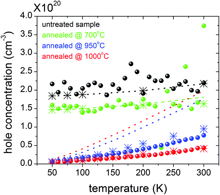 | ||
| Fig. 2 Temperature dependence of the hole concentration for samples: A (untreated), B (annealed at 700 °C), C (annealed at 950 °C) and D (annealed at 1000 °C). The colors for symbols and lines correspond to the samples as indicated in the legend. The mobile hole concentration is shown in dots (experiment) and in stars (calculations). The dotted lines are for the calculated hole concentration within the grain. | ||
Our assumption was additionally confirmed by using the estimated EF to calculate the mobility and the conductivity that were found in agreement with the corresponding data. To interpret the measurements, we further analyzed the mobility and conductivity data. The measured mobility was lower than that theoretically expected for the hole concentration 2 × 1020 cm−3 (Fig. 3). We attributed this to enhanced scattering by ionized impurities (including dopants and defects). The concentration of ionized impurities was estimated at each temperature by fitting the mobility data and is shown in Fig. S2 of the ESI.† These concentrations were used to calculate the conductivity and very good agreement was found with the measured conductivities in the whole T-range (Fig. 3). It is concluded that the transport properties of sample A are fully interpreted by the presence of defects and dominant ionized impurity scattering.
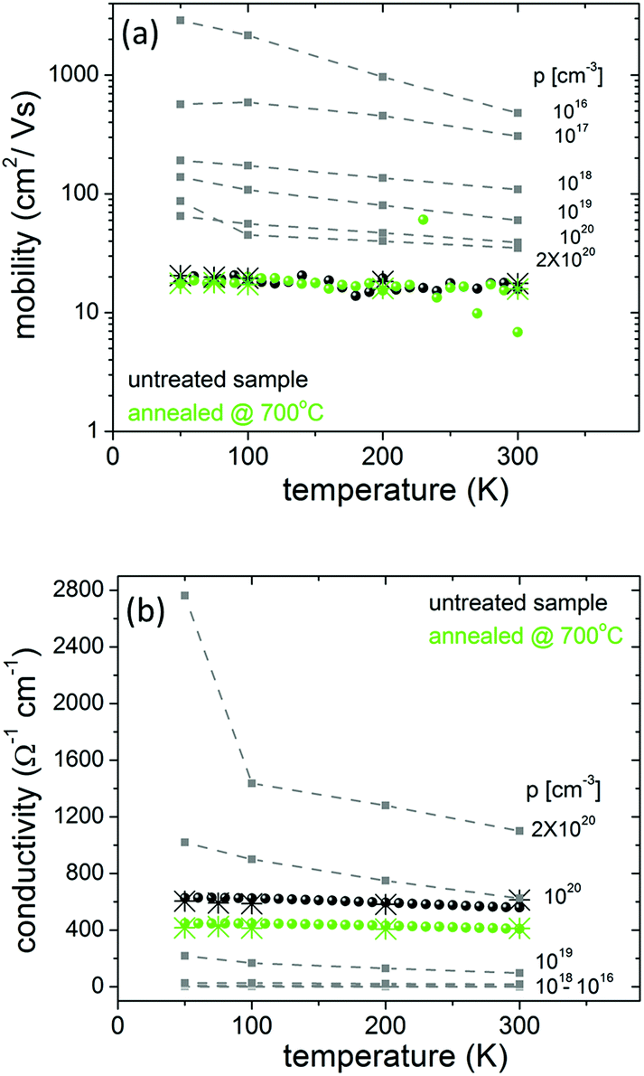 | ||
| Fig. 3 Temperature dependence of (a) the mobility and (b) the conductivity in the low-Ta regime (samples A and B). The dots are for experimental data and the stars are for theoretical calculations. The squares are for the calculated T-dependence of the mobility and the conductivity of bulk Si in a wide hole concentration range shown for reference. The dashed lines are a guide to the eye. | ||
3.2 The formation of energy barriers
Upon thermal annealing at 700 °C (sample B), the hole concentration decreased to ∼1.0 × 1020 cm−3 remaining nearly T-independent (green symbols in Fig. 2). In general terms, thermal post-processing is aimed to facilitate dopant diffusion throughout the material and to annihilate extended defects. Thermal annealing at 700 °C seems indeed to start repairing defects: our theoretical analysis on the hole concentration data indicated a lower impurity concentration in the grains of sample B (Fig. S2†) as well as weaker Fermi level pinning compared to sample A, with EF shifting to −0.06 eV. It should be noted that although the hole concentration and the ionized impurity concentrations are lower in sample B, the mobility is also lower opposing the bulk-like behavior (also shown for reference in Fig. 3). This is explained by the shift of the Fermi level closer to the top of the valence band in sample B compared to sample A. Similar to those of sample A, the mobility data of sample B are very well interpreted by the calculations (Fig. 3). Furthermore, we identified an additional effect of the thermal annealing on the defect distribution across the polycrystalline material, which was of major importance in interpreting the observed thermoelectric behavior. Defects within the grains should repair more easily upon thermal annealing than defects at the grain boundaries where they are more extended. Thus, less defects and hence also less ionized defects would remain in the core of the grains after thermal annealing. This implies that more defects should get ionized at the grain boundaries to satisfy the overall charge neutrality. Ionized defects at the grain boundaries would then form energy barriers for holes and decrease the conductivity. Indeed, a decreased conductivity was measured in sample B after annealing at 700 °C. The measured conductivity was perfectly interpreted in the whole temperature range by assuming the energy barrier height ∼2kBT (Fig. 3). The energy barrier height increases with increasing T because the ionized defect concentration also increases with T. The formation of energy barriers consistently explains the observed increase of the Seebeck coefficient upon thermal annealing (Fig. 5). It can be concluded that thermal annealing at a low Ta decreases the concentration of defects in the grains and acts towards un-pinning the Fermi level. In addition, it increases the concentration of ionized defects at the grain boundaries forming energy barriers for holes.3.3 Scattering mechanism transition
Upon thermal annealing at higher Ta, 950 °C and 1000 °C, a major change was observed in all properties as shown by the hole concentration, mobility and conductivity in samples C and D (Fig. 2 and 4). | ||
| Fig. 4 Temperature dependence of (a) the mobility and (b) the conductivity for the four samples. Dots are for the experiment and stars are for the calculations. | ||
First, the hole concentration decreased significantly upon thermal annealing, also showing a stronger T-dependence compared with samples A and B (Fig. 2). This behavior is explained by the assumed big decrease of defects in the grains upon thermal annealing at high Ta and Fermi level unpinning. Furthermore, mobility is not anymore T-independent as it was in samples A and B due to strong ionized impurity scattering (Fig. 4). It decreases with increasing T as it would be expected due to phonon scattering. Dominant phonon scattering also explains the observed conductivity decrease with increasing T shown in Fig. 4 above a characteristic temperature T* where the conductivity reaches a maximum. The conductivity shows a non-monotonic T-dependence. Below T*, it increases with increasing T. This is because at low temperatures the effect of the increase of the hole concentration with increasing T overcomes the effect of phonon scattering in the conductivity due to a small phonon population. At higher T, the phonon population increases and scatters holes more drastically so that the conductivity decreases with increasing T. The model and the calculations fully interpret the measured mobility and conductivity as can be seen in Fig. 4. It is concluded that a transition from dominant impurity scattering in the grains of samples A and B to dominant phonon scattering in the grains of samples C and D takes place upon thermal annealing at high Ta.
In samples C and D, all transport properties show similar behavior, differing only quantitatively from each other. This indicates that the effects taking place upon thermal annealing are enhanced with increasing Ta. Thermal annealing at higher Ta, decreases more effectively the concentration of defects in the grains and this is why the mobility and conductivity are larger in sample D than in sample C. The gradual dominance of phonon scattering over impurity scattering from sample A to sample D, upon thermal annealing at higher Ta, explains the gradually more pronounced non-monotonic behavior of the conductivity in the samples. Moreover, more defects get ionized at the grain boundaries and higher energy barriers are formed upon thermal annealing at higher Ta. This effect has been included in our modeling by lowering the ionized impurity concentration and increasing the energy barriers in sample D than in sample C. The corresponding parameters have been estimated by fitting the hole concentration and the mobility data. The estimated scatterer concentration is shown in Fig. S1.† The activation energies and the barrier heights were determined by fitting the measured hole concentration in each sample. The barrier height was estimated to be 4kBT in sample C and 5.2kBT in sample D. The defect activation energies were estimated to be 28 meV and 19 meV in samples C and D, respectively, confirming the expectation that defects should be shallower in sample D than in sample C. The conductivity data are thereby interpreted without any further assumptions. Excellent agreement was obtained between the theory and experiment for the mobile hole concentration, the mobility and the conductivity in both samples (Fig. 2 and 4).
3.4 Simultaneous increase of the mobility, conductivity and Seebeck coefficient
The Seebeck coefficient of the samples was measured at 300 K and is shown together with the mobility and the conductivity in Fig. 5.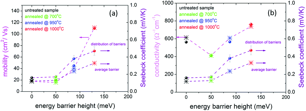 | ||
| Fig. 5 Simultaneous increase of the transport properties for high-Ta. The mobility (left y-axis of (a)), the conductivity (left y-axis of (b)) and the Seebeck coefficient (right y-axes) at 300 K. Dots are for measurements and stars are for calculations. The dashed lines are a guide to the eye. The average energy barrier height for each sample was estimated by the T-dependences of the mobility and conductivity (Fig. 4). | ||
The Seebeck coefficient was calculated for each sample assuming an average barrier height estimated by the T-dependences of the mobility and the conductivity. As seen in the previous sections, the Seebeck coefficient increases with the increasing annealing temperature due to the formation of higher energy barriers at the grain boundaries and more effective energy filtering. This is to be expected. The conductivity though shows an unexpected behavior above a critical annealing temperature. First, it decreases with thermal annealing (the conductivity of sample B is lower than that of the untreated sample A) as expected due to the formation of energy barriers that filter out holes and decrease the mobile hole concentration. This is a well-known effect that takes place upon energy filtering of mobile carriers: the conductivity decreases and the Seebeck coefficient increases. Then, upon thermal annealing at even higher Ta (in samples C and D), the conductivity increases while the energy barriers get gradually higher. This non-conventional behavior is explained by the transition from dominant ionized impurity scattering to dominant phonon scattering in the grains and by the increase of the mobility (as discussed in a previous paragraph). The transition takes place upon the formation of higher energy barriers at the grain boundaries. Therefore, it is concluded that the concurrent scattering mechanism transition and the increasing energy filtering upon thermal annealing explain the simultaneous increase of the mobility, the conductivity and the Seebeck coefficient above a threshold Ta that is estimated to be ∼800 °C.
The Seebeck coefficient of the polycrystalline film, where a distribution of energy barrier heights exists, is larger than that estimated assuming an average energy barrier (respectively shown by dots and stars in Fig. 5). While the effective-grain and average energy barrier are adequate approximations to interpret the conductivity of a polycrystalline material,12 they are not adequate approximations for the Seebeck coefficient, which is more sensitive than the conductivity to the fluctuations of the energy distribution of carriers due to non-uniformity. Thus, for the Seebeck coefficient the effect of non-uniformity cannot be accommodated within the effective medium models assuming an average barrier height or a distribution of barrier heights (e.g. a Gaussian distribution39 and uniform energy distribution of carriers). An extra enhancement of Seebeck coefficient is indeed shown in our nanocrystalline samples. This effect is more pronounced in samples C and D where higher energy barriers are formed upon thermal annealing. The energy distribution of carriers should be sensibly taken into account in a more involved model to provide a fully quantitative interpretation of the Seebeck coefficient data when energy filtering occurs in complex-morphology materials. Our work shows that in such materials, the discrepancy between the measured Seebeck coefficient from the one calculated assuming an average energy barrier estimated by the conductivity and the mobile carrier concentration in the sample, provides a measure of the non-uniform distribution of energy barriers in the material.
4. Conclusions and outlook
By systematic theoretical analysis and interpretation of the T-dependence of the hole transport properties in samples of nc-Si, where a simultaneous increase of the conductivity Seebeck coefficient so far not understood was observed, we identified the mechanisms underlying this behavior. We used effective medium Boltzmann transport theory extended to accommodate energy filtering by energy barriers. The use of an involved model for scattering and the charge neutrality conditions were crucial for quantitatively and consistently interpreting the experimental data. The simulations provided estimations of the involved parameters. The fitting performed throughout the simulation was at each stage subject to validation since multiple properties and dependences had to be non-trivially interpreted. This led to clear evidence of a transition from dominant ionized impurity scattering in the defective grains to dominant phonon scattering upon thermal annealing at higher Ta due to defect repair in the grains. This transition occurs concurrently with the population of more electron traps at grain boundaries so that charge neutrality is fulfilled. Charges at grain boundaries set up energy barriers and energy filtering of carriers. Hence, a unique synergy between charge neutrality and energy filtering activated by the thermal annealing of the originally defective sample leads to a high mobility, conductivity and Seebeck coefficient and a large TPF.The interpretation of the processes underlying the measured remarkable enhancement of the TPF by a factor 15 (i.e. up to 17 mW K−2 m−1) at 300 K can be used to control and optimize the fabrication conditions and prototyping nc-Si with high thermoelectric efficiency. This would meet the aim of enhancing the TPF of Si by a factor of at least 10 to make it competitive for thermoelectric applications and bring technological breakthroughs. Furthermore, our theoretical analysis indicates that the involved physics mechanisms are quite generic and should also take place in other nanostuctured materials if appropriately engineered. Our methodology could serve as guidance to this end. It is interesting to note that the identified synergy takes place in the presence of nanoscale non-uniformity which is here shown capable for both TPF enhancement and decreased thermal conductivity, the two ingredients required for high thermoelectric efficiency.
Conflicts of interest
There are no conflicts to declare.References
- C. B. Vining, The Thermoelectric Properties of Boron-Doped Silicon and Silicon-Germanium in the As-Hot Pressed Conditions, Calif. Inst. of Tech. Technical Report, 1988 Search PubMed.
- C. B. Vining, W. Laskow, J. O. Hanson, R. R. V. der Beck and P. D. Gorsuch, J. Appl. Phys., 1991, 69, 4333 CrossRef CAS.
- Y. Dua, S. Z. Shen, W. Yang, R. Donelson, K. Cai and P. S. Casey, Synth. Met., 2012, 161, 2688 CrossRef.
- C. Liu, J. Xu, B. Lu, R. Yue and F. Kong, J. Electron. Mater., 2012, 41, 639 CrossRef CAS.
- J. Sun, M.-L. Yeh, B. J. Jung, B. Zhang, J. Feser, A. Majumdar and H. E. Katz, Macromolecules, 2010, 43, 2897 CrossRef CAS.
- D. Narducci, E. Selezneva, A. Arcari, G. Cerofolini, E. Romano, R. Tonini and G. Ottaviani, MRS Proc., 2011, 1314 Search PubMed , mrsf10-1314-ll05-16.
- D. Narducci, E. Selezneva, G. F. Cerofolini, S. Fraboni and G. Ottaviani, AIP Conf. Proc., 2012, 1449, 311 CrossRef CAS.
- D. Narducci, E. Selezneva, G. F. Cerofolini, S. Fraboni and G. Ottaviani, J. Solid State Chem., 2012, 193, 19 CrossRef CAS.
- D. Narducci, E. Selezneva, G. Cerofolini, E. Romano, R. Tonini and G. Ottaviani, 8th European Conf. on Thermoelectrics, 2015, pp. 141–146.
- T. Mori and T. Hara, Scr. Mater., 2016, 111, 44 CrossRef CAS.
- R. L. Petritz, Phys. Rev., 1956, 104, 1508 CrossRef CAS.
- J. Y. W. Seto, J. Appl. Phys., 1975, 46, 5247 CrossRef CAS.
- T. Raz, F. Edelman, Y. Komem, M. Stoelzer and P. Zaumseil, J. Appl. Phys., 1998, 84, 4343 CrossRef CAS.
- C. B. Vining and G. D. Mahan, J. Appl. Phys., 1999, 86, 6852 CrossRef CAS.
- M. Ulrich, P. Barnes and C. Vining, J. Appl. Phys., 2001, 90, 1625 CrossRef CAS.
- Y. Kucherov, P. Hagelstein, V. Sevastyanenko, H. L. Brown, S. Guruswamy and W. Wingert, J. Appl. Phys., 2005, 97, 094902 CrossRef.
- J. M. O. Zide, D. Vashaee, Z. X. Bian, G. Zeng, J. E. Bowers, A. Shakouri and A. C. Gossard, Phys. Rev. B: Condens. Matter Mater. Phys., 2006, 74, 205335 CrossRef.
- J. Martin, L. Wang, L. Chen and G. S. Nolas, Phys. Rev. B: Condens. Matter Mater. Phys., 2009, 79, 115311 CrossRef.
- A. J. Minnich, H. Lee, X. W. Wang, G. Joshi, M. S. Dresselhaus, Z. F. Ren, G. Chen and D. Vashaee, Phys. Rev. B: Condens. Matter Mater. Phys., 2009, 80, 155327 CrossRef.
- A. Popescu, L. M. Woods, J. Martin and G. S. Nolas, Phys. Rev. B: Condens. Matter Mater. Phys., 2009, 79, 205302 CrossRef.
- S. K. Bux, R. G. Blair, P. K. Gogna, H. Lee, G. Chen, M. S. Dresselhaus, R. B. Kaner and J.-P. Fleurial, Adv. Funct. Mater., 2009, 19, 2445–2452 CrossRef CAS.
- R. Kim and M. S. Lundstrom, J. Appl. Phys., 2011, 110, 034511 CrossRef.
- M. Bachmann, M. Czerner and C. Heiliger, J. Electron. Mater., 2011, 40, 577 CrossRef CAS.
- M. Bachmann, M. Czerner and C. Heiliger, Phys. Rev. B: Condens. Matter Mater. Phys., 2012, 86, 115320 CrossRef.
- Y. Kajikawa, J. Appl. Phys., 2012, 112, 123713 CrossRef.
- L. P. Scheller and N. H. Nickel, J. Appl. Phys., 2012, 112, 013713 CrossRef.
- A. Samarelli, L. F. Llin, S. Cecchi, J. Frigerio, T. Etzelstorfer, E. Muller, Y. Zhang, J. R. Watling, D. Chrastina, G. Isella, J. Stangl, J. P. Hague, J. M. R. Weaver, P. Dobson and D. J. Paul, J. Appl. Phys., 2013, 113, 233704 CrossRef.
- N. Neophytou, X. Zianni, H. Kosina, S. Frabboni, B. Lorenzi and D. Narducci, Nanotechnology, 2013, 24, 205402 CrossRef.
- D. Narducci, B. Lorenzi, X. Zianni, N. Neophytou, S. Frabboni, G. C. Gazzadi, A. Roncaglia and F. Suriano, Phys. Status Solidi A, 2014, 211, 1255 CrossRef CAS.
- X. Zianni and D. Narducci, J. Appl. Phys., 2015, 117, 035102 CrossRef.
- D. Narducci, S. Frabboni and X. Zianni, J. Mater. Chem. C, 2015, 3, 12176 RSC.
- C. Jacoboni and L. Reggiani, Rev. Mod. Phys., 1983, 55, 645 CrossRef CAS.
- M. Lundstrom, Fundamentals of Carrier transport, Cambridge University Press, 2000 Search PubMed.
- H. Kosina and G. Kaiblinger-Grujin, Solid-State Electron., 1998, 42, 331 CrossRef CAS.
- http://www.ioffe.ru/SVA/NSM/Semicond/ .
- A. Stranz, J. Kaehler, A. Waag and E. Peiner, J. Electron. Mater., 2013, 42, 2381 CrossRef CAS.
- D. J. Chadi, P. H. Citrin, C. H. Park, D. L. Adler, M. A. Marcus and H.-J. Gossmann, Phys. Rev. Lett., 1997, 79, 4834 CrossRef CAS.
- J. Robertson and L. Lin, Technical Digest – International Electron Devices Meeting, 2009, pp. 6.1.1–6.1.4.
- Y. Kajikawa, J. Appl. Phys., 2013, 114, 053707 CrossRef.
Footnote |
| † Electronic supplementary information (ESI) available. See DOI: 10.1039/C8NR09263J |
| This journal is © The Royal Society of Chemistry 2019 |