
 Open Access Article
 This Open Access Article is licensed under a Creative Commons Attribution-Non Commercial 3.0 Unported Licence
High photoresponsivity and broadband photodetection with a band-engineered WSe2/SnSe2 heterostructure†
Hui
Xue
 *a,
Yunyun
Dai
a,
Wonjae
Kim
b,
Yadong
Wang
a,
Xueyin
Bai
a,
Mei
Qi
ac,
Kari
Halonen
a,
Harri
Lipsanen
a and
Zhipei
Sun
ad
*a,
Yunyun
Dai
a,
Wonjae
Kim
b,
Yadong
Wang
a,
Xueyin
Bai
a,
Mei
Qi
ac,
Kari
Halonen
a,
Harri
Lipsanen
a and
Zhipei
Sun
ad
aDepartment of Electronics and Nanoengineering, Aalto University, Espoo 02150, Finland. E-mail: hui.xue@aalto.fi
bVTT Technical Research Center of Finland, Espoo 02150, Finland
cNanobiophotonic Center, State Key Lab Incubation Base of Photoelectric Technology and Functional Materials, International Cooperation Base of Photoelectric Technology and Functional Materials, and Institute of Photonics & Photon-Technology, Northwest University, Xi'an 710069, China
dQTF Centre of Excellence, Department of Applied Physics, Aalto University, FI-00076 Aalto, Finland
First published on 21st January 2019
Abstract
van der Waals (vdW) heterostructures formed by stacking different two-dimensional layered materials have been demonstrated as a promising platform for next-generation photonic and optoelectronic devices due to their tailorable band-engineering properties. Here, we report a high photoresponsivity and broadband photodetector based on a WSe2/SnSe2 heterostructure. By properly biasing the heterostructure, its band structure changes from near-broken band alignment to type-III band alignment which enables high photoresponsivity from visible to telecommunication wavelengths. The highest photoresponsivity and detectivity at 532 nm are ∼588 A W−1 and 4.4 × 10¹⁰ Jones and those at 1550 nm are ∼80 A W−1 and 1.4 × 10¹⁰ Jones, which are superior to those of the current state-of-the-art layered transition metal dichalcogenides based photodetectors under similar measurement conditions. Our work not only provides a new method for designing high-performance broadband photodetectors but also enables a deep understanding of the band engineering technology in the vdW heterostructures possible for other applications, such as modulators and lasers.
Introduction
Recently, two-dimensional (2D) layered materials have received significant attention for photodetection applications due to their high optical absorption,1–10 high carrier mobility and good flexibility.11–16 For example, semiconducting transition metal dichalcogenides (TMDs, such as MoS2, WSe2, MoS2 and MoSe2) are considered as promising candidates for future photodetection applications.17 Indeed, photodetectors with TMDs have been demonstrated with high photoresponsivity (e.g., 800 A W−1 at 561 nm with monolayer MoS2).18 However, the previously reported operation bandwidth of a TMD-based photodetector is typically limited by the bandgap of the TMD material. For example, the bandgap of MoS2 is between ∼1.2 eV (bulk) and ∼1.8 eV (monolayer).19,20 Therefore, in principle, a MoS2 based photodetector typically cannot effectively detect light with a photon energy smaller than 1.2 eV. Such an intrinsic bandgap limitation poses a great challenge for various photonic applications (e.g., telecommunications).van der Waals (vdW) heterojunctions, formed by stacking different individual 2D layered materials, can offer a new dimension in breaking the abovementioned intrinsic bandgap barrier.21–31 In general, three types of band alignments can be categorized when different 2D materials are stacked together,32 including type-I,33 type-II,34–38 and type-III39–43 band alignments. Thus far, most of the reported vdW heterostructure photodetectors are based on the type-II band alignment to utilize the excellent electron–hole pair separation ability in heterostructures. Recently, type-III band alignment has been explored as a platform for tunneling field effect transistors (TFETs) due to its enhanced tunneling current density.40,44–49 The 2D layered materials based type-III band alignment TFETs with improved responsivity and detectivity have been the focus of many recent studies in the visible wavelengths (e.g. 5.7 A W−1 under 660 nm,50 244 A W−1 under 550 nm,51 180 A W−1 under 405 nm![[thin space (1/6-em)]](https://www.rsc.org/images/entities/char_2009.gif) 47). However, the applications of the type-III band alignment TFETs in the field of broadband photodetection have rarely been reported. In this paper, we report a high photoresponsivity and broadband photodetector based on a WSe2/SnSe2 heterostructure. By applying a large negative gate voltage and a reverse bias voltage, the heterojunction band structure changes from type-II to type-III band alignment and a band-to-band tunneling phenomenon occurs. The increased band bending at the heterojunction results in the tunneling-assisted transition which possibly allows photocurrent generation with energy smaller than the bandgap of WSe2 (e.g., 980 nm and 1550 nm) for broadband photodetection (e.g. photo-excited electron tunnel from WSe2 to the conduction band of SnSe2). Under the type-III band alignment conditions, our heterojunction device shows a high photoresponsivity up to ∼588 A W−1 at a wavelength of 532 nm and ∼80 A W−1 at a wavelength of 1550 nm. The corresponding photodetectivity reaches 4.4 × 10¹⁰ Jones and 1.4 × 10¹⁰ Jones for visible and telecommunication wavelengths, respectively.
47). However, the applications of the type-III band alignment TFETs in the field of broadband photodetection have rarely been reported. In this paper, we report a high photoresponsivity and broadband photodetector based on a WSe2/SnSe2 heterostructure. By applying a large negative gate voltage and a reverse bias voltage, the heterojunction band structure changes from type-II to type-III band alignment and a band-to-band tunneling phenomenon occurs. The increased band bending at the heterojunction results in the tunneling-assisted transition which possibly allows photocurrent generation with energy smaller than the bandgap of WSe2 (e.g., 980 nm and 1550 nm) for broadband photodetection (e.g. photo-excited electron tunnel from WSe2 to the conduction band of SnSe2). Under the type-III band alignment conditions, our heterojunction device shows a high photoresponsivity up to ∼588 A W−1 at a wavelength of 532 nm and ∼80 A W−1 at a wavelength of 1550 nm. The corresponding photodetectivity reaches 4.4 × 10¹⁰ Jones and 1.4 × 10¹⁰ Jones for visible and telecommunication wavelengths, respectively.
Results and discussion
The optical image and schematic illustration of the WSe2/SnSe2 heterostructure device are shown in Fig. 1a. Few-layer p-type WSe2 and n-type SnSe2 flakes, mechanically exfoliated from their bulk materials, are transferred onto a 280 nm SiO2/silicon substrate. An overlapping heterojunction region is formed by precisely controlling their locations. Pd/Au metal contacts (20/50 nm) are patterned onto the WSe2 and SnSe2 flakes to collect holes and electrons. The thicknesses of the WSe2 and SnSe2 few-layer flakes are determined by atomic force microscopy (AFM), giving the values of 6 nm and 15 nm, respectively (ESI Fig. S1†). Raman spectroscopy is employed to confirm the high quality of our device after the fabrication processes (ESI Fig. S2†).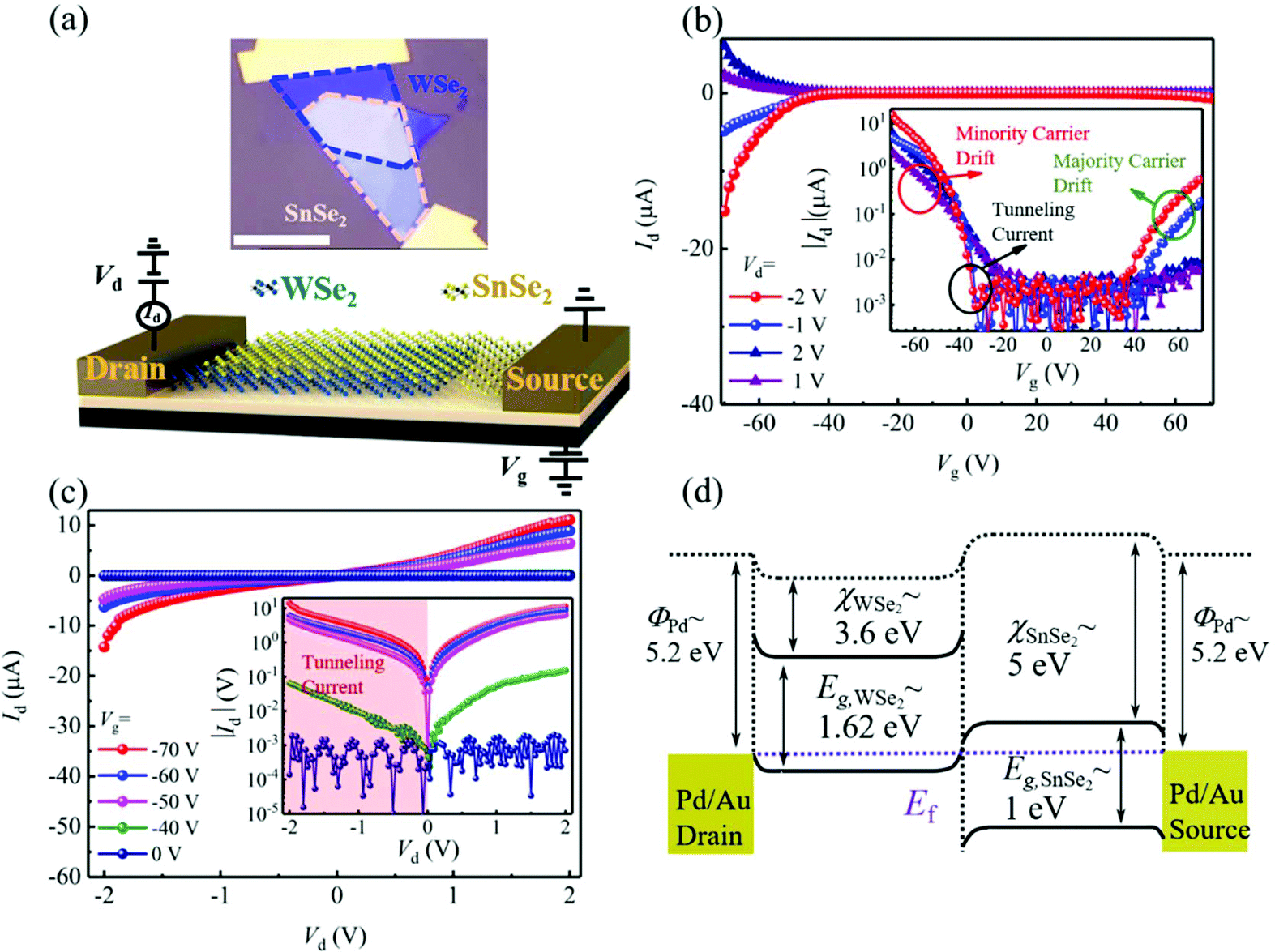 | ||
| Fig. 1 The WSe2/SnSe2 heterostructure device and its electronic properties. (a) Microscopy image (upper panel) and schematic illustration (bottom panel) of the heterojunction device. (b) Id–Vg characteristics measured with variable Vd in the dark. Inset: |Id|–Vg characteristics on the logarithmic scale. (c) Id–Vd characteristics measured with variable Vg in the dark. Inset: |Id|–Vd characteristics on the logarithmic scale. (d) The schematic band diagrams of the heterojunction. The scale bar is 10 μm. | ||
Before testing the electrical characteristics of the WSe2/SnSe2 heterostructure, we also fabricated two individual WSe2 and SnSe2 based field effect transistors (FETs) to analyze the properties of WSe2 and SnSe2. WSe2 and SnSe2 FETs are fabricated on Si/SiO2 substrates with Pd/Au (20/50 nm) as the drain and source electrodes. The transfer curves of the FETs (ESI Fig. S3†) show p-type characteristics for WSe2 and n-type characteristics for SnSe2, indicating that Pd can efficiently inject holes into WSe2 and electrons into SnSe2 when a negative gate voltage is applied.41,52 Moreover, the nonlinear output results of the WSe2 flake (ESI Fig. S3b†) indicate the existence of a Schottky barrier at the contact region, while the SnSe2 results (ESI Fig. S3d†) indicate that an ohmic contact is formed between Pd and SnSe2. Note that, since SnSe2 is a degenerated n-doped semiconductor, the band alignment of SnSe2 at the interface would be relatively unaffected by the Vg (see ESI Fig. S3c†).35,43
Next, the electronic properties of the WSe2/SnSe2 heterojunction is studied. The device is characterized by applying a constant drain to source voltage (Vd) and a gate voltage (Vg) in the configuration shown in Fig. 1a. The device shows obvious p-type transport characteristics. The concentration and the type of the carriers can be tuned by Vg, at Vd = −2 V; the Id–Vg result shows the gate-controlled current, with an on–off ratio of ∼104 (see Fig. 1b). The reverse current (Ireverse, Vd < 0 V) at Vg < −30 V is the band-to-band tunneling (BTBT) current, whose magnitude increases as the gate voltage decreases. The magnitude of Ireverse at Vg > 40 V increases as the gate voltage increases due to the majority carrier drifting. The forward current (Iforward, Vd > 0 V) observed at Vg < −30 V can be attributed to the drifting of the minority carriers (see the discussion below). The magnitude of the reverse current increases with both positive and negative Vg and the maximum of the reverse current is 15 μA when Vd = −2 V and Vg = −70 V. The gate-dependent current–voltage (Id–Vd) characteristics are shown in Fig. 1c, where two important features can be observed. First, owing to the ultrathin thickness nature of the heterojunction, the magnitude of both Iforward and Ireverse can be significantly controlled by modifying the gate voltage. Second, since the breakdown voltage (i.e. −0.01 V) is very much less than 4Eg/q, where Eg is the band gap of the semiconductors (1.62 eV of WSe2 and 1 eV of SnSe2) and q is the electron charge, the tunneling current (red region in the inset of Fig. 1c) can be attributed to Zener tunneling.53
The qualitative band alignment of the WSe2/SnSe2 heterostructure at zero bias is sketched in Fig. 1d based on the reported electron affinity values in the literature.54,55 Based on these values, a nearly broken band alignment is formed, where the Fermi level of WSe2 locates at the edge of its valence band and that of SnSe2 locates at the edge of its conduction band. The heterostructure resembles a p–n diode with a staggered band gap offset. The bottom of the conduction band and the top of the valence band of WSe2 (SnSe2) are at 3.6 eV (5.22 eV) and 5 eV (6 eV), so that the offsets of the conduction band and valence band are about 1.4 eV and 0.78 eV, respectively.
The transfer characteristics of the heterostructure can be understood through band diagrams (Fig. 2a–c). When there is no gate voltage (i.e. Vg = 0 V), as shown in Fig. 2(a), the high Schottky barrier at the drain contact and the high difference of the conduction/valence band discontinuity restrain the current flow, leading to the zero dark current. Under these conditions, the device can be seen as a Schottky diode in series with a p–n junction and a resistor. When a negative gate voltage is applied (i.e. Vg < −30 V) as shown in ESI Fig. S3b,† the doping level of WSe2 is increased and a near-ohmic contact is formed at the drain contact (the band bending direction at the drain contact shifts downwards). Thus, the model of the device under these conditions can be described as two resistors in series with a p+n junction. Therefore, when a reverse bias is applied (Fig. 2b), the valence band maximum of WSe2 shifts above the conduction band minimum of SnSe2, and the type of the band structure changes from near broken band alignment to broken band alignment (type-III). Thus, the electrons in the valence band of WSe2 can tunnel into the conduction band of the SnSe2 flake. This tunneling current can then be increased by increasing the reverse bias voltage, see Fig. 1c, due to the enlarged overlapping energy level between the valence band of WSe2 and the conduction band of SnSe2. However, when a forward bias is applied (Fig. 2c), the band alignment changes from type-III to type-II, the barrier height at the heterojunction is reduced, and the majority carriers (electrons in SnSe2 and holes in WSe2) can overcome the interface barrier and drift to their counterparts, leading to a high forward current. The carrier transportation under the forward bias conditions follows the mechanism as described for the traditional p–n diode, where the forward current increases exponentially with forward bias.40 To further analyze the transfer characteristics of the heterostructure, scanning photocurrent mapping at λ = 532 nm under a confocal optical microscope (objective 100×, NA = 0.75, Plaser = 50 μW (corresponding to a power intensity of 8.5 × 10³ W cm−2)) was performed, as shown in Fig. 2d–f. The spot size (∼0.6 μm2 at 532 nm) of the incident laser is much smaller than the size (∼50 μm2) of the heterojunction. When there is no bias (i.e. Vg = Vd = 0 V), as mentioned above, the heterostructure resembles a p–n junction. Thus, when there is an external light excitation, electron–hole pairs will be generated and separated efficiently at the heterojunction (Fig. 2d) where the photo-generated electrons move to the SnSe2 flake while the holes move to the WSe2 flake, due to the built-in electric field.56 The part of the heterojunction near the drain contact shows a stronger photocurrent, which has also been observed in ref. 57, and can be attributed to the lower sheet resistance of this region compared to those of other parts. Note that the photocurrent mapping results only indicate the region where the dominant photocurrent is generated. A small photocurrent (e.g., ∼1 nA in Fig. 2d) can be observed in the drain part of the device. Under reverse bias with a negative Vg, the Id is governed by the BTBT, where carriers from the valence band of the WSe2 tunnel move to the conduction band of SnSe2, as mentioned above (Fig. 2b). Since the reversed Vd enhances the electric field in the heterojunction area, Fig. 2e exhibits a larger Iph (∼50 times larger than that in Fig. 2d) throughout the entire heterojunction. In contrast, while the device is at forward bias with a negative gate voltage, Pd can efficiently inject holes into WSe2, which can overcome the thermionic barrier and reach the source contact. In addition, the band bending at the heterojunction is released, leading to small Iph generation in the heterojunction (Fig. 2f). Due to the fact that the direction of the built-in field at the drain part is the same as that of the external field, around Iph = 1 μA is generated at the drain contact and the direction is towards the drain part.
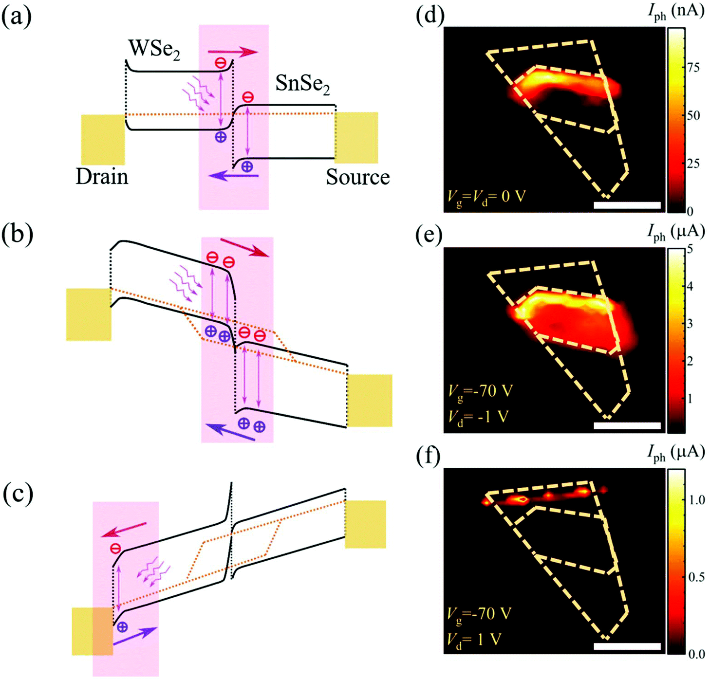 | ||
| Fig. 2 Operation principle of our heterojunction device. (a–c) Band diagram of heterojunction and Schottky junctions, where (a) Vg = Vd = 0 V, (b) Vg = −70 V, Vd = −1 V and (c) Vg = −70 V, Vd = 1 V. The red/purple arrows indicate the carrier movement direction. The magenta arrows indicate the separation process of electron–hole pairs. The pink rectangular regions indicate the position of the strongest built-in electric field. (d–f) Photocurrent mapping of the heterojunction under different bias conditions at 532 nm. Plaser = 50 μW (8.5 × 10³ W cm−2). The dashed lines outline the flakes and heterojunction. The scale bar is 10 μm. | ||
The detailed photoresponse behavior of our device under a λ = 532 nm laser is also studied (Fig. 3). Note that, all the measurements are carried out by locating the laser spot at the heterojunction where the largest photocurrent is generated (Fig. 2e). The time-dependent Iph under pulsed light illumination (λ = 532 nm, 10 μW) is firstly tested at Vg = 0 V and −70 V with different bias voltages, respectively, shown in Fig. 3a. The steep rise and fall edges indicate the fast response of the device. The device shows the photodiode-like behavior, where the Iph increases significantly when it is at reverse bias compared with that of forward bias both at Vg = 0 V and −70 V. This can be explained by the fact that the increased band bending under the reverse bias conditions results in the efficient separation of the photo-generated electron–hole pairs, which coincides with our photocurrent mapping results (Fig. 2e and f). Since the forward bias results in a much lower Iph compared with that from reverse bias, in the following discussion we will only focus on the Iph under the condition of the reverse bias voltage.
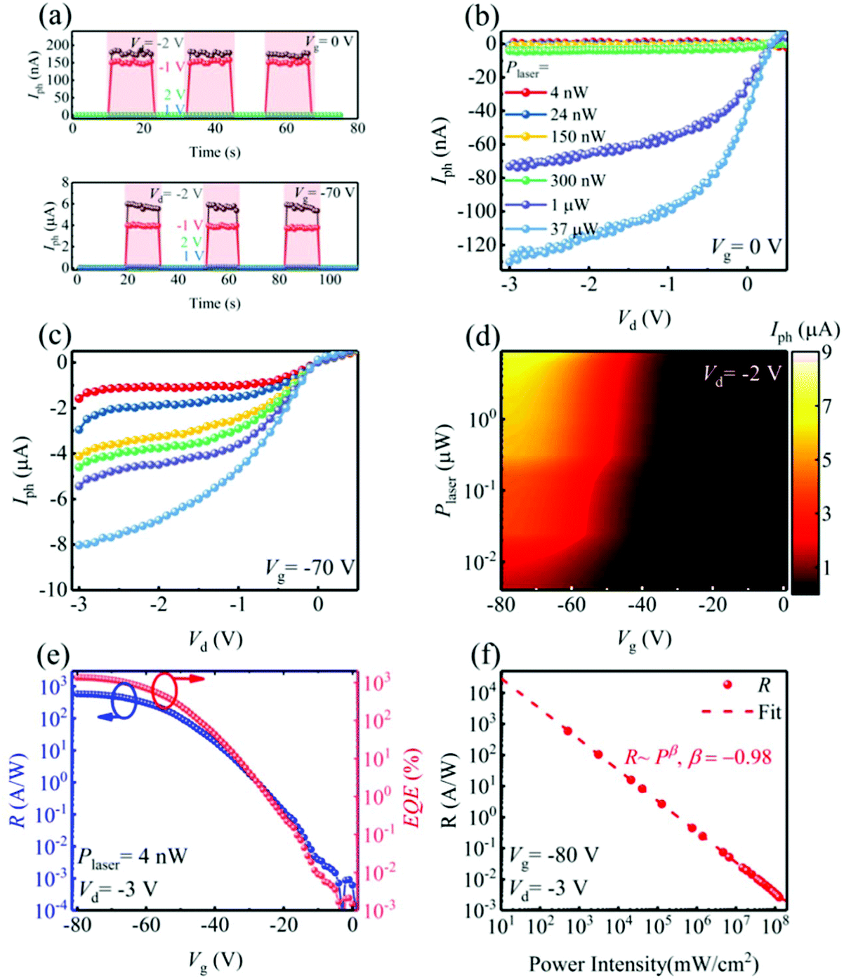 | ||
| Fig. 3 Photoresponse of the WSe2/SnSe2 heterojunction device at 532 nm. (a) Photo-switching characteristics at different Vd. Iph–Vd characterization of the WSe2/SnSe2 heterojunction at (b) Vg = 0 V and (c) Vg = −70 V. (d) Iph dependence of the Vg and Plaser. (e) R and EQE dependence of Vg. (f) R measured with different input power intensities. | ||
Fig. 3b and c illustrate the Iph–Vd curves of the heterostructure with fixed gate voltages (Vg = 0 V and Vg = −70 V, respectively) under the λ = 532 nm laser with the laser power varying from 4 nW to 37 μW. The magnitude of the Iph strongly depends on the Vd, due to the increased carrier drift velocity and the increased charge carrier separation efficiency, suggesting that a higher photocurrent can be readily achieved by applying a larger reversed Vd. With the increase in the Plaser, the Iph at reverse bias increases and approaches 8 μA at Vd = −3 V and Vg = −70 V (Fig. 3c). Moreover, since the larger reversed Vd and Vg will lead to the larger electric field at the heterojunction region, the efficiency of the photo-excited carrier separation increases, resulting in a ∼62-fold increase of Iph (Plaser = 37 μW, Vd = −3 V) at Vg = −70 V compared with that at Vg = 0 V. The Iph as a function of Vg and Plaser is plotted in Fig. 3d. Clearly, the Iph increases with the decreasing of the gate voltage and a higher incident laser power. For example, when Plaser = 1 μW, the photocurrent is remarkable (∼2 μA) under the condition of Vg < −40 V, confirming that a smaller Vg leads to a larger photocurrent.
To better understand the photoresponse properties of our device, several important figures of merit for photodetectors are studied, including the photoresponsivity (R = Iph/Plaser), detectivity (D = R × s1/2/(2 × q × Idark)1/2) and external quantum efficiency (EQE = (Iph/q)/(Plaser/hυ)), where q is the electron charge, s is the illumination area, Idark is the current when the laser is off and hυ is the photon energy.17 The gate-dependent R and EQE are shown in Fig. 3e. With a decrease in the Vg, the largest R and EQE could reach 588 A W−1 and 1367%, respectively, benefitting from the increased band bending which has been mentioned above. An EQE larger than 100% has been previously observed, which is might due to the photo-excited carriers being recirculated many times before reaching the electrodes resulting from the long carrier lifetime.50,58 The highest D is estimated to be 4.4 × 10¹⁰ Jones. The corresponding R as a function of the incident power intensity is summarized in Fig. 3f. It is clearly observed that the R linearly changes with the Plaser in the log scale. By fitting the experimental data with the equation of R ∼ Pβ, the term β is obtained at −0.98 for 532 nm, indicating the superior photocurrent capability and excellent separation efficiency of photo-induced charge carriers.
Telecommunication wavelength detection is an important issue for various applications. Here, we test our heterojunction device at telecommunication wavelengths. The spatially resolved photocurrent mapping with a λ = 1550 nm laser (Vd = −1 V, Vg = −70 V and Plaser = 10 μW) reveals pronounced photocurrent generation in the overlapped region (Fig. 4a). Fig. 4b and c depict the gate-dependent photoresponse of the device under 980 nm and 1550 nm lasers, where Iph shows the same tendency as that at 532 nm. However, a threshold for the near-infrared photon detection can be observed. For example, under the bias conditions, Vd = −2 V and Plaser = 10 μW, for λ = 980 nm, the photocurrent is not detectable when the Vg is larger than −60 V. As for the incident light at λ = 1550 nm, under the same bias conditions, this threshold voltage shifts to Vg = −70 V. This fascinating phenomenon can be attributed to the tunneling-assisted transition in the band-bending heterojunction: an extremely negative gate voltage and a high reverse bias voltage increase the built-in electric field at the heterojunction, and the edges of the conduction band and valence band are tilted along the direction of the electric field. The electron and hole wave functions have a tail which extends into the band gap, enhancing the e–h interactions with sub-bandgap photons.59 Thus, under such a high built-in electric field, our device has the potential to allow the photo-excited carrier generation with a photon energy smaller than the intrinsic band-gap of WSe2 and transfer to the conduction band of SnSe2.53,60 The magnitude of the photocurrent under the 980 nm laser is around 2.6 times larger than that generated under the 1550 nm laser because the photon energy of 980 nm is higher than that of 1550 nm. Note that there is no photoresponse of our device when it is forward biased even when the device is exposed to an intense light. Fig. 4d and e show the Iph–Vd curves of the heterostructure with a fixed gate voltage (Vg = −70 V) under the λ = 980 nm and 1550 nm lasers with the laser power varying from 6 nW to 400 μW and 17 nW to 400 μW, respectively. The magnitude of the Iph shows strong dependence on the reverse bias voltage. This results from the larger built-in electric field at the larger reverse bias voltage. Fig. 4f depicts the R of the device under λ = 980 and 1550 nm as a function of the laser intensity. The maximum R of our device (according to the fitting results) is 396 A W−1 at 980 nm (Plaser = 100 mW cm−2) and is 80 A W−1 at 1550 nm (Plaser = 100 mW cm−2). The R at the visible wavelength and telecommunication wavelength range is superior to those of the previously reported 2D materials and their heterostructure based photodetectors (see ESI Fig. S4†). The highest detectivity and EQE at these two wavelengths are 4.4 × 10¹⁰ Jones, 500% and 1.4 × 10¹⁰ Jones, 64%, respectively. The time-dependent Iph under pulsed light illumination (at 1550 nm) is determined (ESI Fig. S5†). The rise time and the decay time are 16 and 45 ms, respectively. We believe that the speed of the device can be further improved by improving the crystal quality.
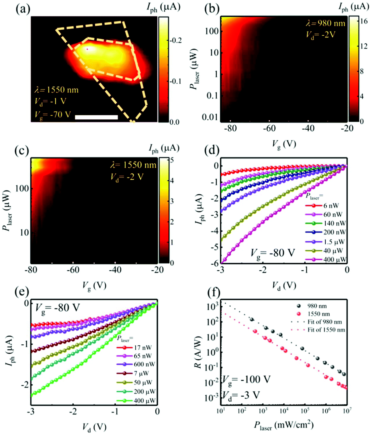 | ||
| Fig. 4 Photoresponse of the WSe2/SnSe2 heterojunction device at 980 nm and 1550 nm. (a) Photocurrent mapping of the heterojunction under different bias conditions at 1550 nm. Plaser = 10 μW (2 × 10⁵ mW cm−2). Iph dependence of the Vg and Plaser at (b) 980 nm and (c) 1550 nm. Iph–Vd characterization of the WSe2/SnSe2 heterojunction at (d) 980 nm and (e) 1550 nm. (f) R at different input power intensities. The scale bar is 10 μm. | ||
Conclusions
In summary, we report a high-sensitivity and broadband few-layer WSe2/SnSe2 heterostructure based photodetector. The band-to-band tunneling mechanism allows the proposed device to detect light from visible to telecommunication wavelengths. The highest responsivity and detectivity at 532 nm are 588 A W−1 and 4.4 × 10¹⁰ Jones and those at 1550 nm are 80 A W−1 and 1.4 × 10¹⁰ Jones, which outperform the state-of-art 2D materials based photodetectors. Our work shows an attractive platform for practical applications of utilizing few-layer TMD based heterojunctions for high-performance optoelectronic devices (such as modulators61,62 and lasers).63–68Conflicts of interest
There are no conflicts to declare.Acknowledgements
We acknowledge funding from the Academy of Finland (Grant No. 276376, 284548, 295777, 304666, 312551, 314810, and 320167), the Academy of Finland Centre of Excellence program (project 312297), the Academy of Finland Flagship program (project 320167), Business Finland (OPEC, A-photonics), the European Union's Seventh Framework Program (Grant No. 631610), the European Union's Horizon 2020 research and innovation programme (Grant No. 820423, S2QUIP), Aalto Centre of Quantum Engineering, China Scholarship Council, and the provision of technical facilities of the Micronova, Nanofabrication Centre of Aalto University.References
- J. Wang, H. Fang, X. Wang, X. Chen, W. Lu and W. Hu, Small, 2017, 13, 1700894 CrossRef PubMed.
- J. Liang, J. Zhang, Z. Li, H. Hong, J. Wang, Z. Zhang, X. Zhou, R. Qiao, J. Xu, P. Gao, Z. Liu, Z. Liu, Z. Sun, S. Meng, K. Liu and D. Yu, Nano Lett., 2017, 17, 7539–7543 CrossRef CAS PubMed.
- A. Saynatjoki, L. Karvonen, H. Rostami, A. Autere, S. Mehravar, A. Lombardo, R. A. Norwood, T. Hasan, N. Peyghambarian, H. Lipsanen, K. Kieu, A. C. Ferrari, M. Polini and Z. Sun, Nat. Commun., 2017, 8, 893 CrossRef PubMed.
- H. Yang, H. Jussila, A. Autere, H. P. Komsa, G. J. Ye, X. H. Chen, T. Hasan and Z. P. Sun, ACS Photonics, 2017, 4, 3023–3030 CrossRef CAS.
- H. Hu, X. Yang, F. Zhai, D. Hu, R. Liu, K. Liu, Z. Sun and Q. Dai, Nat. Commun., 2016, 7, 12334 CrossRef CAS PubMed.
- Z. Q. Luo, D. D. Wu, B. Xu, H. Y. Xu, Z. P. Cai, J. Peng, J. Weng, S. Xu, C. H. Zhu, F. Q. Wang, Z. P. Sun and H. Zhang, Nanoscale, 2016, 8, 1066–1072 RSC.
- A. Martinez and Z. P. Sun, Nat. Photonics, 2013, 7, 842–845 CrossRef CAS.
- A. Autere, C. R. Ryder, A. Saynatjoki, L. Karvonen, B. Amirsolaimani, R. A. Norwood, N. Peyghambarian, K. Kieu, H. Lipsanen, M. C. Hersam and Z. P. Sun, J. Phys. Chem. Lett., 2017, 8, 1343–1350 CrossRef CAS PubMed.
- P. Yan, H. Chen, J. Yin, Z. Xu, J. Li, Z. Jiang, W. Zhang, J. Wang, I. L. Li, Z. Sun and S. Ruan, Nanoscale, 2017, 9, 1871–1877 RSC.
- H. Jussila, H. Yang, N. Granqvist and Z. P. Sun, Optica, 2016, 3, 151–158 CrossRef CAS.
- S. Das, R. Gulotty, A. V. Sumant and A. Roelofs, Nano Lett., 2014, 14, 2861–2866 CrossRef CAS PubMed.
- F. Bonaccorso, Z. Sun, T. Hasan and A. C. Ferrari, Nat. Photonics, 2010, 4, 611–622 CrossRef CAS.
- A. C. Ferrari, F. Bonaccorso, V. Fal'ko, K. S. Novoselov, S. Roche, P. Boggild, S. Borini, F. H. Koppens, V. Palermo, N. Pugno, J. A. Garrido, R. Sordan, A. Bianco, L. Ballerini, M. Prato, E. Lidorikis, J. Kivioja, C. Marinelli, T. Ryhanen, A. Morpurgo, J. N. Coleman, V. Nicolosi, L. Colombo, A. Fert, M. Garcia-Hernandez, A. Bachtold, G. F. Schneider, F. Guinea, C. Dekker, M. Barbone, Z. Sun, C. Galiotis, A. N. Grigorenko, G. Konstantatos, A. Kis, M. Katsnelson, L. Vandersypen, A. Loiseau, V. Morandi, D. Neumaier, E. Treossi, V. Pellegrini, M. Polini, A. Tredicucci, G. M. Williams, B. H. Hong, J. H. Ahn, J. M. Kim, H. Zirath, B. J. van Wees, H. van der Zant, L. Occhipinti, A. Di Matteo, I. A. Kinloch, T. Seyller, E. Quesnel, X. Feng, K. Teo, N. Rupesinghe, P. Hakonen, S. R. Neil, Q. Tannock, T. Lofwander and J. Kinaret, Nanoscale, 2015, 7, 4598–4810 RSC.
- T. Juntunen, H. Jussila, M. Ruoho, S. H. Liu, G. H. Hu, T. Albrow-Owen, L. W. T. Ng, R. C. T. Howe, T. Hasan, Z. P. Sun and I. Tittonen, Adv. Funct. Mater., 2018, 28, 1800480 CrossRef.
- S. Li, Y. C. Lin, W. Zhao, J. Wu, Z. Wang, Z. Hu, Y. Shen, D. M. Tang, J. Wang, Q. Zhang, H. Zhu, L. Chu, W. Zhao, C. Liu, Z. Sun, T. Taniguchi, M. Osada, W. Chen, Q. H. Xu, A. T. S. Wee, K. Suenaga, F. Ding and G. Eda, Nat. Mater., 2018, 17, 535–542 CrossRef CAS PubMed.
- F. Bonaccorso, A. Lombardo, T. Hasan, Z. Sun, L. Colombo and A. C. Ferrari, Mater. Today, 2012, 15, 564–589 CrossRef CAS.
- Z. H. Sun and H. X. Chang, ACS Nano, 2014, 8, 4133–4156 CrossRef CAS PubMed.
- O. Lopez-Sanchez, D. Lembke, M. Kayci, A. Radenovic and A. Kis, Nat. Nanotechnol., 2013, 8, 497–501 CrossRef CAS PubMed.
- K. K. Kam and B. A. Parkinson, J. Phys. Chem. A, 1982, 86, 463–467 CrossRef CAS.
- K. F. Mak, C. Lee, J. Hone, J. Shan and T. F. Heinz, Phys. Rev. Lett., 2010, 105, 136805 CrossRef PubMed.
- A. K. Geim and I. V. Grigorieva, Nature, 2013, 499, 419–425 CrossRef CAS PubMed.
- W. Zhang, Q. Wang, Y. Chen, Z. Wang and A. T. S. Wee, 2D Mater., 2016, 3, 022001 CrossRef.
- H. Qiao, J. Yuan, Z. Q. Xu, C. Y. Chen, S. H. Lin, Y. S. Wang, J. C. Song, Y. Liu, Q. Khan, H. Y. Hoh, C. X. Pan, S. J. Li and Q. L. Bao, ACS Nano, 2015, 9, 1886–1894 CrossRef CAS PubMed.
- K. Zhang, T. Zhang, G. Cheng, T. Li, S. Wang, W. Wei, X. Zhou, W. Yu, Y. Sun, P. Wang, D. Zhang, C. Zeng, X. Wang, W. Hu, H. J. Fan, G. Shen, X. Chen, X. Duan, K. Chang and N. Dai, ACS Nano, 2016, 10, 3852–3858 CrossRef CAS PubMed.
- W. Kim, S. Arpiainen, H. Xue, M. Soikkeli, M. Qi, Z. Sun, H. Lipsanen, F. A. Chaves, D. Jimenez and M. Prunnila, ACS Appl. Nano Mater., 2018, 1, 3895–3902 CrossRef CAS PubMed.
- X. Yang, Z. Sun, T. Low, H. Hu, X. Guo, F. J. Garcia de Abajo, P. Avouris and Q. Dai, Adv. Mater., 2018, 30, e1704896 CrossRef PubMed.
- H. Hu, X. Guo, D. Hu, Z. Sun, X. Yang and Q. Dai, Adv. Sci., 2018, 5, 1800175 CrossRef PubMed.
- D. Hu, X. Yang, C. Li, R. Liu, Z. Yao, H. Hu, S. N. G. Corder, J. Chen, Z. Sun, M. Liu and Q. Dai, Nat. Commun., 2017, 8, 1471 CrossRef PubMed.
- X. Yang, F. Zhai, H. Hu, D. Hu, R. Liu, S. Zhang, M. Sun, Z. Sun, J. Chen and Q. Dai, Adv. Mater., 2016, 28, 2931–2938 CrossRef CAS PubMed.
- H. Chen, J. Yin, J. Yang, X. Zhang, M. Liu, Z. Jiang, J. Wang, Z. Sun, T. Guo, W. Liu and P. Yan, Opt. Lett., 2017, 42, 4279–4282 CrossRef PubMed.
- G. Hu, T. Albrow-Owen, X. Jin, A. Ali, Y. Hu, R. C. T. Howe, K. Shehzad, Z. Yang, X. Zhu, R. I. Woodward, T.-C. Wu, H. Jussila, J.-B. Wu, P. Peng, P.-H. Tan, Z. Sun, E. J. R. Kelleher, M. Zhang, Y. Xu and T. Hasan, Nat. Commun., 2017, 8, 278 CrossRef PubMed.
- V. O. Ozcelik, J. G. Azadani, C. Yang, S. J. Koester and T. Low, Phys. Rev. B, 2016, 94, 035125 CrossRef.
- J. W. Lee, Y. J. Choi, J. M. Yang, S. Ham, S. K. Jeon, J. Y. Lee, Y. H. Song, E. K. Ji, D. H. Yoon, S. Seo, H. Shin, G. S. Han, H. S. Jung, D. Kim and N. G. Park, ACS Nano, 2017, 11, 3311–3319 CrossRef CAS PubMed.
- D. Jariwala, S. L. Howell, K. S. Chen, J. Kang, V. K. Sangwan, S. A. Filippone, R. Turrisi, T. J. Marks, L. J. Lauhon and M. C. Hersam, Nano Lett., 2016, 16, 497–503 CrossRef CAS PubMed.
- X. Zhou, N. Zhou, C. Li, H. Song, Q. Zhang, X. Hu, L. Gan, H. Li, J. Lü, J. Luo, J. Xiong and T. Zhai, 2D Mater., 2017, 4, 025048 CrossRef.
- L. Ye, H. Li, Z. Chen and J. Xu, ACS Photonics, 2016, 3, 692–699 CrossRef CAS.
- M. Buscema, J. O. Island, D. J. Groenendijk, S. I. Blanter, G. A. Steele, H. S. van der Zant and A. Castellanos-Gomez, Chem. Soc. Rev., 2015, 44, 3691–3718 RSC.
- H. Xue, Y. Wang, Y. Dai, W. Kim, H. Jussila, M. Qi, J. Susoma, Z. Ren, Q. Dai, J. Zhao, K. Halonen, H. Lipsanen, X. Wang, X. Gan and Z. Sun, Adv. Funct. Mater., 2018, 1804388 CrossRef.
- K. E. Aretouli, D. Tsoutsou, P. Tsipas, J. Marquez-Velasco, S. A. Giamini, N. Kelaidis, V. Psycharis and A. Dimoulas, ACS Appl. Mater. Interfaces, 2016, 8, 23222–23229 CrossRef CAS PubMed.
- X. Liu, D. Qu, H. M. Li, I. Moon, F. Ahmed, C. Kim, M. Lee, Y. Choi, J. H. Cho, J. C. Hone and W. J. Yoo, ACS Nano, 2017, 11, 9143–9150 CrossRef CAS PubMed.
- T. Roy, M. Tosun, M. Hettick, G. H. Ahn, C. Hu and A. Javey, Appl. Phys. Lett., 2016, 108, 083111 CrossRef.
- C. Li, X. Yan, X. Song, W. Bao, S. Ding, D. W. Zhang and P. Zhou, Nanotechnology, 2017, 28, 415201 CrossRef PubMed.
- X. Yan, C. Liu, C. Li, W. Bao, S. Ding, D. W. Zhang and P. Zhou, Small, 2017, 13, 1701478 CrossRef PubMed.
- M. Li, D. Esseni, J. J. Nahas, D. Jena and H. G. Xing, IEEE J. Electron Devices Soc., 2015, 3, 206–213 Search PubMed.
- A. Nourbakhsh, A. Zubair, M. S. Dresselhaus and T. Palacios, Nano Lett., 2016, 16, 1359–1366 CrossRef CAS PubMed.
- D. Tan, X. Wang, W. Zhang, H. E. Lim, K. Shinokita, Y. Miyauchi, M. Maruyama, S. Okada and K. Matsuda, Small, 2018, 14, e1704559 CrossRef PubMed.
- Q. A. Vu, J. H. Lee, V. L. Nguyen, Y. S. Shin, S. C. Lim, K. Lee, J. Heo, S. Park, K. Kim, Y. H. Lee and W. J. Yu, Nano Lett., 2017, 17, 453–459 CrossRef CAS PubMed.
- R. Yan, S. Fathipour, Y. Han, B. Song, S. Xiao, M. Li, N. Ma, V. Protasenko, D. A. Muller, D. Jena and H. G. Xing, Nano Lett., 2015, 15, 5791–5798 CrossRef CAS PubMed.
- K. Murali and K. Majumdar, IEEE J. Electron Devices Soc., 2018, 65, 4141–4148 Search PubMed.
- C. Lan, C. Li, S. Wang, T. He, T. Jiao, D. Wei, W. Jing, L. Li and Y. Liu, ACS Appl. Mater. Interfaces, 2016, 8, 18375–18382 CrossRef CAS PubMed.
- X. Zhou, X. Hu, S. Zhou, H. Song, Q. Zhang, L. Pi, L. Li, H. Li, J. Lu and T. Zhai, Adv. Mater., 2018, 30, 1703286 CrossRef PubMed.
- W. Zhang, M.-H. Chiu, C.-H. Chen, W. Chen, L.-J. Li and A. T. S. Wee, ACS Nano, 2014, 8, 8653–8661 CrossRef CAS PubMed.
- J. I. Pankove, Optical processes in semiconductors, Prentice-Hall, Englewood Cliffs, N.J, 1971 Search PubMed.
- X. Duan, C. Wang, A. Pan, R. Yu and X. Duan, Chem. Soc. Rev., 2015, 44, 8859–8876 RSC.
- Y. Guo and J. Robertson, Appl. Phys. Lett., 2016, 108, 233104 CrossRef.
- M. Buscema, D. J. Groenendijk, G. A. Steele, H. S. van der Zant and A. Castellanos-Gomez, Nat. Nanotechnol., 2014, 5, 4651 CAS.
- Y. Deng, Z. Luo, N. J. Conrad, H. Liu, Y. Gong, S. Najmaei, P. M. Ajayan, J. Lou, X. Xu and P. D. Ye, ACS Nano, 2014, 8, 8292–8299 CrossRef CAS PubMed.
- G. Konstantatos, M. Badioli, L. Gaudreau, J. Osmond, M. Bernechea, F. P. Garcia de Arquer, F. Gatti and F. H. Koppens, Nat. Nanotechnol., 2012, 7, 363–368 CrossRef CAS PubMed.
- J. B. You, H. Kwon, J. Kim, H. H. Park and K. Yu, Opt. Express, 2017, 25, 4284–4297 CrossRef CAS PubMed.
- Y. Zhou, Y. H. Liu, J. Cheng and Y. H. Lo, Nano Lett., 2012, 12, 5929–5935 CrossRef CAS PubMed.
- Z. Sun, A. Martinez and F. Wang, Nat. Photonics, 2016, 10, 227–238 CrossRef CAS.
- A. Autere, H. Jussila, A. Marini, J. R. M. Saavedra, Y. Y. Dai, A. Saynatjoki, L. Karvonen, H. Yang, B. Amirsolaimani, R. A. Norwood, N. Peyghambarian, H. Lipsanen, K. Kieu, F. J. G. de Abajo and Z. P. Sun, Phys. Rev. B, 2018, 98, 115426 CrossRef.
- Z. Sun, T. Hasan and A. C. Ferrari, Phys. E, 2012, 44, 1082–1091 CrossRef CAS.
- Z. P. Sun, T. Hasan, F. Torrisi, D. Popa, G. Privitera, F. Q. Wang, F. Bonaccorso, D. M. Basko and A. C. Ferrari, ACS Nano, 2010, 4, 803–810 CrossRef CAS PubMed.
- F. Bonaccorso and Z. P. Sun, Opt. Mater. Express, 2014, 4, 63–78 CrossRef.
- J. Bogusławski, Y. Wang, H. Xue, X. Yang, D. Mao, X. Gan, Z. Ren, J. Zhao, Q. Dai, G. Soboń, J. Sotor and Z. Sun, Adv. Funct. Mater., 2018, 28, 1801539 CrossRef.
- A. Autere, H. Jussila, Y. Dai, Y. Wang, H. Lipsanen and Z. Sun, Adv. Mater., 2018, 30, 1705963 CrossRef PubMed.
- D. A. Li, H. Jussila, L. Karvonen, G. J. Ye, H. Lipsanen, X. H. Chen and Z. P. Sun, Sci. Rep., 2015, 5, 15899 CrossRef CAS PubMed.
Footnote |
| † Electronic supplementary information (ESI) available: (1) AFM image of a heterostructure, (2) Raman spectra of the heterostructure, (3) electrical characteristics of WSe2 and SnSe2 based FETs, (4) photoresponsivity comparison of this work and previous results, (5) photo-switching characteristics of the device. See DOI: 10.1039/c8nr09248f |
| This journal is © The Royal Society of Chemistry 2019 |