
 Open Access Article
 This Open Access Article is licensed under a Creative Commons Attribution-Non Commercial 3.0 Unported Licence
Fabrication of multi-material 3D structures by the integration of direct laser writing and MEMS stencil patterning†
Jeremy B.
Reeves
*a,
Rachael K.
Jayne
 *b,
Lawrence
Barrett
c,
Alice E.
White
bcde and
David J.
Bishop
*abcde
*b,
Lawrence
Barrett
c,
Alice E.
White
bcde and
David J.
Bishop
*abcde
aDepartment of Electrical and Computer Engineering, Boston University, Boston, Massachusetts 02215, USA. E-mail: djb1@bu.edu
bDepartment of Mechanical Engineering, Boston University, Boston, Massachusetts 02215, USA
cDivision of Materials Science and Engineering, Boston University, Boston, Massachusetts 02215, USA
dDepartment of Physics, Boston University, Boston, Massachusetts 02215, USA
eDepartment of Biomedical Engineering, Boston University, Boston, Massachusetts 02215, USA
First published on 4th February 2019
Abstract
The construction of a complex, 3D optical metamaterial challenges conventional nanofabrication techniques. These metamaterials require patterning of both a deformable mechanical substrate and an optically-active structure with ∼200 nm resolution and precision. The soft nature of the deformable mechanical materials often precludes the use of resist-based techniques for patterning. Furthermore, FIB deposition approaches produce metallic structures with considerable disorder and impurities, impairing their optical response. In this paper we discuss a novel solution to this nanofabrication challenge – the integration of direct laser writing and MEMS stencil patterning. We demonstrate a variety of methods that enable this integration and then show how one can produce optically-active, 3D metamaterials. We present optical characterization data on one of these metamaterials to demonstrate the viability of our nanofabrication approach.
1. Introduction
The construction of 3D optical metamaterials is a significant nanofabrication challenge. One typically needs to pattern both the mechanical substrate as well as the optically-active elements, each with deep sub-micron resolution, and then align them relative to each other, also with deep sub-micron precision. A powerful approach for fabricating the mechanical layer is direct laser writing (DLW) via two-photon polymerization (TPP). DLW provides a method for the fabrication of complex 3D shapes with arbitrary geometries and minimum feature sizes of ∼200 nm. This technique enables rapid prototyping of virtually any nanoscale structure, and has been used to produce nanolattices, sensors and actuators, photonic crystals, and metamaterials.1–5 Currently, the materials compatible with DLW are largely limited to dielectric polymers.In many cases, DLW-fabricated structures often serve as a starting point for multi-material integration. DLW works by focusing laser into a photosensitive material to induce a TPP reaction at the focal spot, which, in the case of a negative photoresist, results in an ovoid-shaped solid with submicron resolution. By moving the position of the laser focus, complex 3D structures can be realized. When integrating other materials, DLW structures typically behave as a scaffold for coating a desired final material including ceramics6 and metals,2,3,7,8 allowing for the creation of structures with geometries that are not practical using planar lithographic methods. Fabricating mechanical,9 magnetic,10 and optical metamaterials1,11 with properties derived from the microscale 3D geometries enabled by DLW remains a fruitful line of research. So far, much of this work has been limited to conformal coating of DLW structures. Methods for selective patterning of DLW structures or integration of non-polymer materials have remained somewhat limited. While procedures based on two-photon reduction and metal-ion doped polymers have produced useful devices and structures,12–14 combining DLW with established patterning and deposition techniques will allow for complex multi-material and material-agnostic fabrication processes. Applications will include 3D optical metamaterials as described below and the construction of 3D scaffolds with embedded biosensors for tissue engineering.
Previously, we reported the selective patterning of metallic split-ring resonators (SRRs) on a mechanically flexible 3D structure.15 Despite the resolution achieved and the underlying complex 3D structure of the device, the surface on which metallic patterning was performed was 2D. Here, we demonstrate that extending the stencil lithographic technique to 3D multilayer microstructures allows for the creation of optical metamaterials with a response enhanced by the custom-designed 3D architecture.
We present a method for selective patterning of metallic structures onto 3D polymer microstructures. Complex 3D structures are printed via DLW and then patterned with metallic features using microelectromechanical systems (MEMS) stencils and electron-beam evaporation. By implementing multiple stencil lithography steps, it is possible to build each layer out of independent patterns and materials. The procedure is schematically outlined in Fig. 1(a–f). The benefits of using this stencil technique over existing methods are that the stencil process frees the design of 3D-structures from constraints associated with geometries and chemistries of traditional planar lithography or two-photon reduction for the fabrication of metallic features. Other materials and physical vapor deposition (PVD) methods can also be used with the technique including processes for depositing organic molecules such as organic vapor jet printing.16
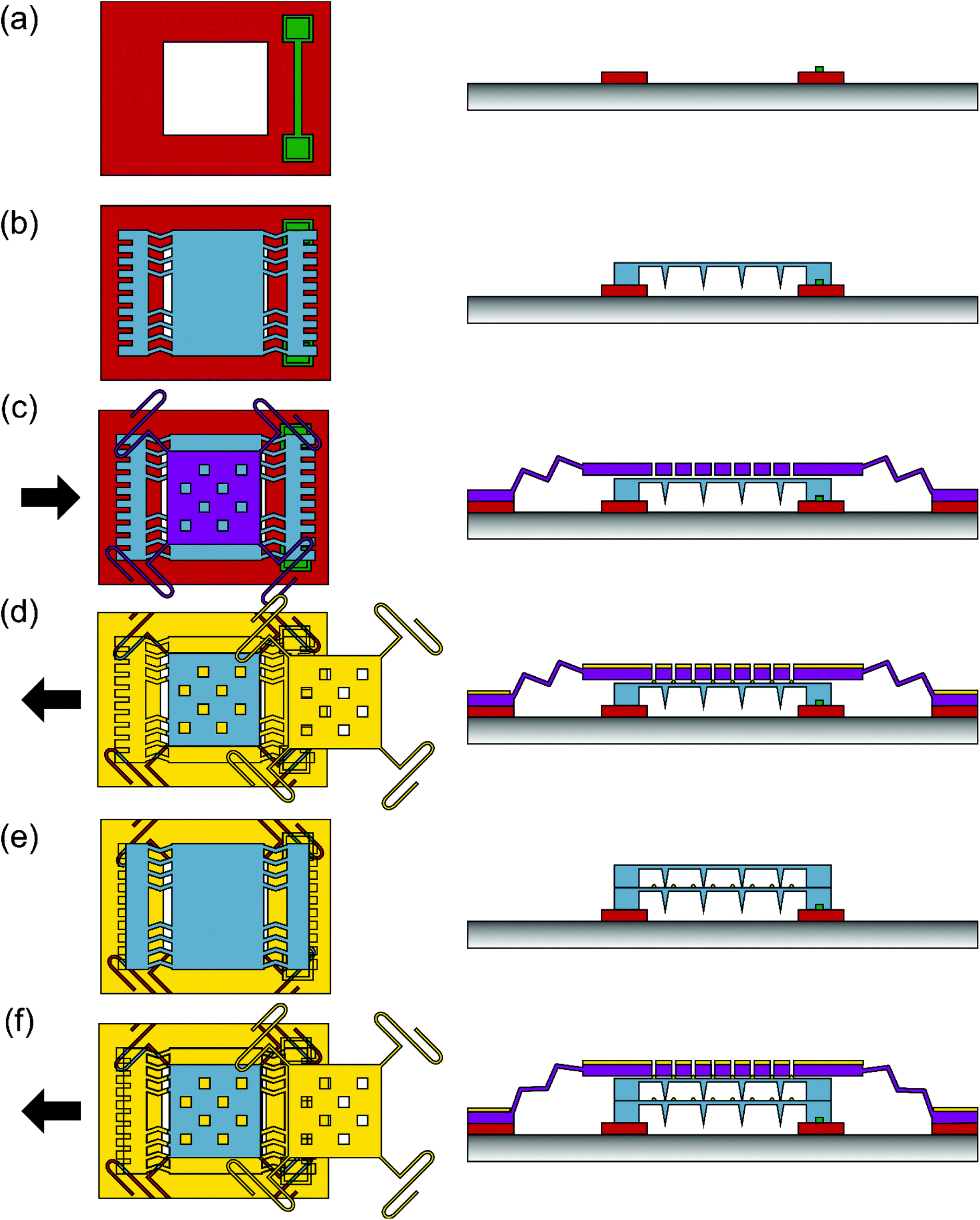 | ||
| Fig. 1 Schematic showing the top (left column) and side (right column) views of the multistep process for fabricating 3D metal–polymer structures. (a) The mobile substrate (red) with raised “dumbbell” structure (green) for polymer are shown. (b) The 3D DLW structure (blue) is printed onto the mobile substrate. (c) Next, the mobile substrate is repositioned so that the DLW structure is aligned underneath the stencil mask (purple). (d) Metal (yellow) is evaporated through the mask using electron beam, then the mobile substrate is removed from underneath the mask and placed in it's original position. (e) Another DLW structure is fabricated. (f) The positioning and deposition processes are repeated. | ||
2. Results and discussion
To test the feasibility of multi-layer selective patterning on 3D polymer microstructures, we chose the DLW structure designs shown in Fig. 1(b). The design of these structures have several key features. In order to minimize surface roughness, the flat central area of the structure intended for metallic deposition is printed with a small hatch value, which means that for each subsequent line, the laser focus overlaps significantly with the previous line. To prevent the printed layer from curling up and detaching from the surface due to minimal post-processing shrinkage, deformable polymer springs attach the flat central area to the anchors on either side. With the central flat area suspended, small posts on the underside of the flat sheet reduce stiction. Furthermore, the side anchors have “teeth” to maximize surface area, thereby enhancing contact/cross polymerization when the subsequent layer is printed. The spacing between the two layers is limited by resist bubbling caused by local heating that arises when patterned metallic elements are irradiated by the laser focus. Metallic elements can be completely encapsulated by the DLW polymer material, but there is a trade-off between the polymerization power that can be used before local bubbling near the surface of the metal, and structure shrinkage from underpolymerization. In this study, we found that a spacing of ∼2 μm is sufficient to prevent bubble formation.MEMS mechanical elements are used both to manipulate the 3D structure and to position the mask for electron-beam evaporation. The devices used in this study are shown in Fig. 2. All MEMS devices used here are fabricated using the PolyMUMPS process at the MEMSCAP foundry.17 PolyMUMPS allows for two mechanically movable layers, referred to as poly-1 (P1) and poly-2 (P2). Generally, these layers make up the mask (P2) and carrier (P1) layer for the fabrication of micro-patterned multi-layer DLW structures. The MEMS stencil mask layer is similar to that of Atomic Calligraphy,18 where masks are suspended by soft silicon springs to enable better alignment with 3D structures. The carrier layer is capable of acting as a mobile substrate for the 3D-structures, and can be moved independently of the mask layer. The inclusion of this mobile substrate is important for repositioning the 3D structures under various stencil masks.
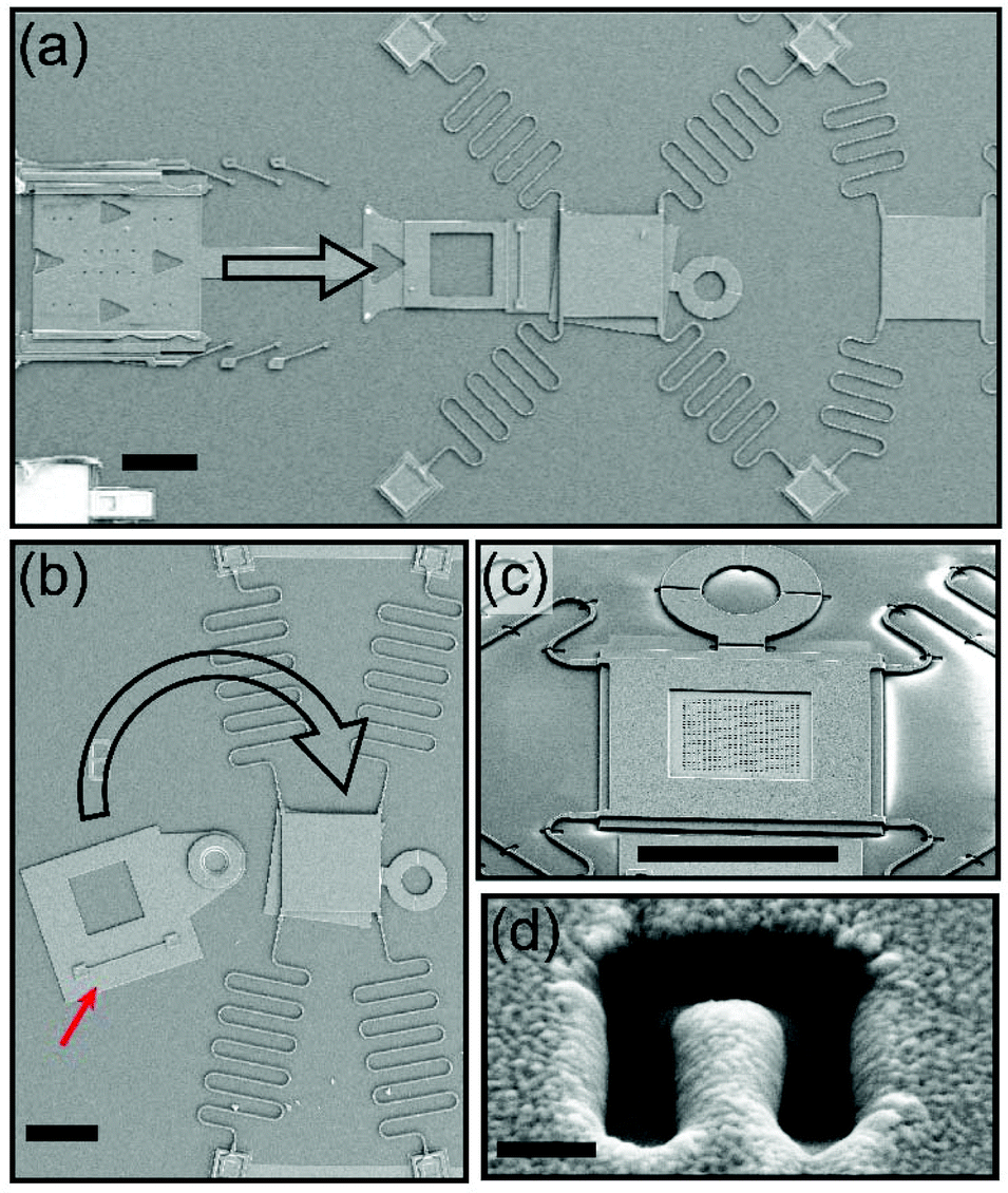 | ||
| Fig. 2 MEMS devices and FIB-processing of MEMS stencil masks. (a) A sliding shuttle design with two spring tethered masks for multiple mask patterns (b) rotating plate design with raised “dumbbell” structure (arrow). (c) FIB patterned stencil area on a mask plate. (d) Single repeated element of stencil mask pattern. To maximize pattern resolution, the polysilicon is thinned in the FIB to about 300 nm. (Scale bars represent 100, 100, 100, and 0.5 μm respectively.) | ||
We explore the utility of two possible mobile substrate designs in multilayer printing. The first, a sliding shuttle seen in Fig. 2(a), can be aligned with two separate mask plates to provide the movable substrate for the 3D structure. This allows positioning of the shuttle under the first mask to pattern the first layer of the DLW structure. After a metallic deposition step, the shuttle is returned to its initial position and a second DLW step prints another polymer layer on top of the first. The shuttle and mask device layers are manipulated using a probe station. It is important to note that in this demonstration, we have designed specifically to accommodate two unique masks so each layer can be patterned independently, but it is possible to include more masks in this series if needed. For example, one might imagine a very long mask plate with an array of stencil designs etched along the long axis, and a mobile shuttle designed to “snap in” at various positions along this elongated mask depending on the stencil needed.
A second mobile substrate design, shown in Fig. 2(b), relies on a rotating hinge to reposition a DLW-fabricated structure beneath a mask. By simply rotating the mobile substrate ∼180 degrees, the mobile substrate can be positioned beneath the mask. Manipulation of the mask-hinge system is easier compared to the sliding shuttle design because this mobile substrate is fixed to the MEMS substrate. The specific design addressed here is limited to a single mask pattern and could be used to create repeating stacks of independent layers. In principal, this design could accommodate a variety of masks if the MEMS tether and mask are designed appropriately.
In order to produce stencil masks with features smaller than the 2 μm critical dimension of the foundry process, patterns were milled into the foundry-fabricated mask plates using focused-ion beam (FIB). This allows for stencil patterns with feature sizes below 0.5 μm with resolution of ∼200 nm. The 1.25 μm-thick P2 plate is thinned to about 300 nm before a stencil pattern is milled through the plate. The resulting patterns have attained features well below 1 μm.
The MEMS devices arrive from the foundry encapsulated in a sacrificial oxide. FIB patterning and the first DLW printing is performed directly on the unreleased MEMS die. DLW printing is carried out using the Nanoscribe Photonics Professional GT with a 63×, NA = 1.4 immersion objective and IP-Dip photoresist. To remove unpolymerized photoresist, samples are submerged in propylene glycol monomethyl acetate (PGMEA, Sigma Aldrich) for at least 20 minutes, then dipped in NOVEC 2100 (3M) to remove residual PGMEA. After processing, the device is then released by submersion in hydrofluoric acid and undergoes critical point drying. The raised dumbbell-shaped structures on the mobile substrate (Fig. 2(b), red arrow) provide a strong attachment point for the 3D structures, improving device yield of the release step to nearly 100%.
To pattern the DLW structures printed on MEMS carriers, a probe station is used to position the DLW structures below the patterned stencil masks and PVD of the selected material is performed. After deposition, the mobile substrate is returned to its initial position. For subsequent layers, another DLW structure is printed directly onto the existing patterned structure and the patterning process repeats. To prevent structures from floating away during the DLW printing and processing steps, it is important that the mobile substrates maintain their contact with the base substrate. For example, the shuttle mobile substrates must be repositioned in the guiding rails seen in Fig. 2(a).
The results of all process steps are shown in Fig. 3, which shows a device with two layers of aluminum-patterned IP-Dip. The movable shuttle has been replaced to its initial position. As seen in Fig. 3(b–c), both layers have identical SRR patterns deposited on their surface and the separation between the layers is ∼2 μm. Because the surface of the 3D structure to be patterned is flat, the mask is in close contact with the surface, allowing for accurate reproduction of the stencil pattern in aluminum on the surface. The SRR in Fig. 3(d) shows straight sidewalls and negligible surface diffusion, which indicate that geometric spread and diffusion typically associated with stencil lithography can be controlled. Fig. 3(e) indicates good adhesion between the first and second DLW-printed layers.
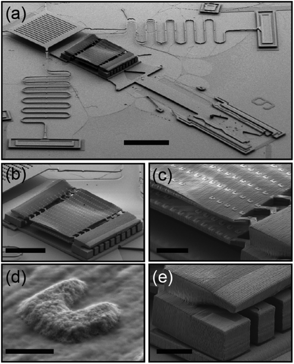 | ||
| Fig. 3 Fabricated multilayer structures. (a) The patterned, multilayer structure positioned back in the initial shuttle position after a second aluminum deposition step. (b) The double layer structure. (c) Close-up of the separated, patterned layers. (d) Close-up of an individual split-ring structure. (e) Close-up of the joint between the first and second DLL layers showing good polymer–polymer adhesion. (Scale bars represent 100, 50, 10, 1, and 10 μm respectively.) | ||
As shown in Fig. 4, full design flexibility in optical metamaterials requires the ability to orient the SRRs in any of three directions in space. In general, there are two main fundamental resonances, magnetic dipole with current circulating around the SRR and electric dipole with current running across the arms of the SRR. The magnetic dipole is excited when the electric field is directed across the gap (in the y-direction for SRR-x or in the x-direction for SRR-y in Fig. 4), or when the magnetic flux penetrates the ring, which occurs when the electric field and Poynting vector are in the plane of the SRR. The electric dipole will be excited anytime the electric field is parallel to the SRR arms (along x, y, or z for SRR-x, SRR-y, or SRR-z, respectively). Optical response from the SRR depends on the specific relative orientations between the incident optical field and the SRR. The table in Fig. 4 shows the 18 combinations of SRR, Poynting vector and polarization orientations and the coupling of light to the magnetic dipole resonance. A full discussion of the geometry of SRR orientations relative to the Poynting vector of incident light is not appropriate here, but overall, the ability to engineer a strong response to any specific configuration of incident light requires that one be able to rotate the SRRs around all three axes.
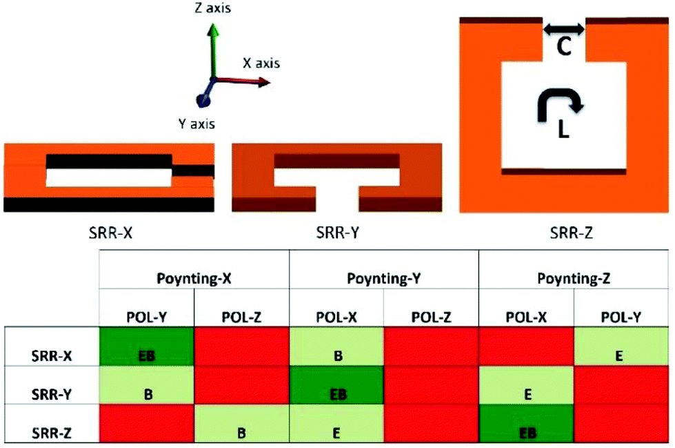 | ||
| Fig. 4 Shown are the 18 combinations of SRR, Poynting vector and polarization orientations and the coupling of light to the magnetic dipole resonance. In the nomenclature used here SRR-X,Y,Z refers to the orientation of the SRR as shown above, Poynting-X,Y,Z refers to the direction of the Poynting vector of the light incident on the SRR and POL-X,Y,Z refers to the linear polarization of that light. The table indicates the coupling between the incident light and the SRR. Green indicates strong coupling (to both E and B fields), light green indicates weak coupling (only E or B field alone), and red indicates no coupling. | ||
In order to characterize the quality of the metallic patterns fabricated on each layer in the multi-deposition experiments, we fabricate a two-layer structure with 23 × 23 arrays of gold 1.2 μm square split-ring resonators on each layer, as seen in Fig. 5(a). The SRR orientation is rotated by 90 degrees between the two layers in order to distinguish their optical responses. The split rings in Fig. 5(b) are fabricated using the shuttle mobile substrate in Fig. 2(a), with each mask plate having an array of differently oriented resonators. We note that the structure demonstrated in Fig. 5(a) has a slight curvature to the upper surface. This can be attributed to bubbles, which were generated in the resist during the second DLW step, moving the polymerized layers as the structure prints. These bubbles can be prevented by suspending the adjacent layer by at least 2 μm above any patterned regions. We further note that because both masks are exposed to the atomic flux during subsequent evaporations, the upper layer has slightly narrower features due to partial filling of the mask pattern by the deposited metal.
 | ||
Fig. 5 Fabricated multi-material structures with optical response in the mid-infrared. (a) The fabricated multilayer structure. (b) SEM image of a gold split ring resonator from the first layer (top image) and the second layer (bottom image) of the two-layer stack. A single layer device consists only of the split rings on the first layer. (c) Schematic of the multi-layer structure with relative split ring orientations. (d) Reflection spectrum of a single (left) and double (right) layer structures showing the fundamental magnetic and electric resonances of the split ring structures. Spectra for light polarized along ŷ (![[x with combining circumflex]](https://www.rsc.org/images/entities/i_char_0078_0302.gif) ) are plotted in solid red (dashed blue). The scale bars in (a) and (b) correspond to 100 and 0.5 μm respectively. ) are plotted in solid red (dashed blue). The scale bars in (a) and (b) correspond to 100 and 0.5 μm respectively. | ||
We measure the optical response of this structure using a Fourier-transform infrared spectrometer with attached microscope in reflection mode (Bruker Hyperion 1000). Each structure is illuminated by light polarized along the or ŷ axes. The single-layer device (represented by only the lower layer of the two-layer devices) exhibits two resonances, as seen in Fig. 5(d), corresponding to the fundamental electric and magnetic dipole resonances of the SRRs around 4 μm and 8 μm respectively.19 As the Poynting vector is perpendicular to the planes containing the SRRs, each resonance driven by the electric field is individually excited by orthogonal polarizations of the infrared radiation. The multilayer structure demonstrates similar resonances; however, the spectra do not display the same polarization sensitivity as is seen in the single layer device. Both layers of the 3D-structure contribute to the optical response. While IP-Dip is an excellent resist for high resolution DLW fabrication, its acrylate formulation contributes to strong absorption features around 5 μm and 8 μm.15 These features are particularly noticeable in the multilayer structure since the light must pass through the IP-Dip structure after being reflected.
The data in Fig. 5 clearly demonstrates that one can use this integrated approach to build 3D optical metamaterials. The use of an epoxy-based resist such as SU-8 may avoid some of these sharp infrared absorptions while still allowing high resolution DLW.20,21 Avoiding such lossy features or designing the metallic pattern for resonances in other spectral regions will lead to the fabrication of high performance metamaterials and surfaces.
Having freedom to fabricate the SRR in any of the configurations in Fig. 4 could lead to metamaterials with isotropic, polarization-insensitive responses. Using the methods described here, a DLW structure with a 5 × 5 array of 10 μm cubic cutouts was patterned with aluminum SRRs (Fig. 6(a) and (b)). The mask was aligned so that each SRR stencil pattern sat on top of a single cubic cutout. Proper registration between these two components is achieved through the inclusion of self-alignment posts on the DLW-fabricated 3D structures and corresponding alignment apertures on the MEMS stencil. Instead of stacking layers of selectively-patterned DLW structures, subsequent angled deposition steps through this MEMS stencil were used to deposit nanoscale patterns on all five of the internal side walls of the cubic cutouts using the approach shown in Fig. 6(c) and (d), demonstrating full flexibility in how the SRRs are oriented. Between deposition steps, no mask repositioning is necessary and just the device orientation relative to the PVD source is changed. The alignment posts on the mechanical layer determine the registry of the MEMS mask layer to a precision of a few hundred nanometers, thus eliminating the need for any kind of optical alignment step. The foreshortening effects on the vertical sidewalls are predictable and can be corrected for in the design of the apertures in the stencil.
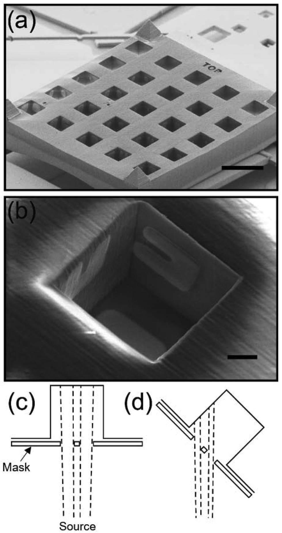 | ||
| Fig. 6 Shown in (a) and (b) are results using the approach described in Fig. 1, 2, 3 to produce a structure where the SRRs are oriented in all three directions, like the sketch in Fig. 4. The DLW structure was designed to have alignment posts (visible at the corners of the structure) which were used to align the MEMS mask. Scale bars are 20 μm and 2 μm respectively. Schematics are shown for (c) 0° deposition angle used to pattern the bottom face of the cubic cutout and (d) 45° deposition angles to pattern the side faces. | ||
3. Conclusions
We have demonstrated a method integrating DLW and MEMs stencil lithography to build multi-material 3D structures. DLW 3D structures can be patterned with metallic nanostructures to produce optical metamaterials with useful geometries that are nearly polarization insensitive. This technique offers more material flexibility than comparable techniques such as two-photon reduction, and enables high-resolution selective patterning of 3D DLW structures in a field that has largely relied on conformal coatings. Additional studies will investigate the possibility of using non-planar DLW substrates in tandem with techniques like angled deposition to enhance the complexity of structures that can be fabricated using this approach.Conflicts of interest
There are no conflicts to declare.Acknowledgements
This work was funded by Boston University Photonics Center, Boston University College of Engineering, the DARPA Atoms to Product (A2P) Program/Air Force Research Laboratory (AFRL) contract no. FA8650-15-C-7545, NSF-CMMI-1361948 and the NSF ERC Program under Cooperative Agreement No. EEC-1647837.Notes and references
- M. S. Rill, C. Plet, M. Thiel, I. Staude, G. Von Freymann, S. Linden and M. Wegener, Nat. Mater., 2008, 7, 543–546 CrossRef CAS PubMed.
- F. Formanek, N. Takeyasu, T. Tanaka, K. Chiyoda, A. Ishikawa and S. Kawata, Opt. Express, 2006, 14, 800 CrossRef CAS PubMed.
- V. Mizeikis, S. Juodkazis, R. Tarozaite, J. Juodkazyte, K. Juodkazis and H. Misawa, Opt. Express, 2007, 15, 8454–8464 CrossRef CAS PubMed.
- F. Klein, T. Striebel, J. Fischer, Z. Jiang, C. M. Franz, G. Von Freymann, M. Wegener and M. Bastmeyer, Adv. Mater., 2010, 22, 868–871 CrossRef CAS PubMed.
- M. Deubel, G. Von Freymann, M. Wegener, S. Pereira, K. Busch and C. M. Soukoulis, Nat. Mater., 2004, 3, 444–447 CrossRef CAS PubMed.
- D. Jang, L. R. Meza, F. Greer and J. R. Greer, Nat. Mater., 2013, 12, 893–898 CrossRef CAS PubMed.
- K. M. Huang, S. C. Tsai, Y. K. Lee, C. K. Yuan, Y. C. Chang, H. L. Chiu, T. T. Chung and Y. C. Liao, RSC Adv., 2017, 7, 51663–51669 RSC.
- N. Takeyasu, T. Tanaka and S. Kawata, Appl. Phys. A: Mater. Sci. Process., 2008, 90, 205–209 CrossRef CAS.
- L. R. Meza, A. J. Zelhofer, N. Clarke, A. J. Mateos, D. M. Kochmann and J. R. Greer, Proc. Natl. Acad. Sci. U. S. A., 2015, 112, 11502–11507 CrossRef CAS PubMed.
- G. Williams, M. Hunt, B. Boehm, A. May, M. Taverne, D. Ho, S. Giblin, D. Read, J. Rarity, R. Allenspach and S. Ladak, Nano Res., 2018, 11, 845–854 CrossRef.
- J. K. Gansel, M. Thiel, M. S. Rill, M. Decker, K. Bade, V. Saile, G. Von Freymann, S. Linden and M. Wegener, Science, 2009, 325, 1513–1515 CrossRef CAS PubMed.
- X. M. Duan, H. B. Sun, K. Kaneko and S. Kawata, Thin Solid Films, 2004, 453–454, 518–521 CrossRef CAS.
- S. Tabrizi, Y. Cao, B. P. Cumming, B. Jia and M. Gu, Adv. Opt. Mater., 2016, 4, 529–533 CrossRef CAS.
- S. Tabrizi, Y. Y. Cao, H. Lin and B. H. Jia, Sci. China: Phys., Mech. Astron., 2017, 60, 1–17 CAS.
- J. B. Reeves, R. K. Jayne, T. J. Stark, L. K. Barrett, A. E. White and D. J. Bishop, Nano Lett., 2018, 18, 2802–2806 CrossRef CAS PubMed.
- M. Shtein and S. R. Forrest, United States Patent and Trademark Office, US7431968B1, 2008, Oct, 26 Search PubMed.
- D. Koester, A. Cowen and R. Mahadevan, PolyMUMPs Design Handbook, MEMSCAP Inc, 2013 Search PubMed.
- M. Imboden, H. Han, J. Chang, F. Pardo, C. A. Bolle, E. Lowell and D. J. Bishop, Nano Lett., 2013, 13, 3379–3384 CrossRef CAS PubMed.
- C. Rockstuhl, F. Lederer, C. Etrich, T. Zentgraf, J. Kuhl and H. Giessen, Opt. Express, 2006, 14, 8827 CrossRef PubMed.
- D. B. Fullager, G. D. Boreman and T. Hofmann, Opt. Mater. Express, 2017, 7, 888 CrossRef CAS.
- S. Juodkazis, V. Mizeikis, K. K. Seet, M. Miwa and H. Misawa, Nanotechnology, 2005, 16, 846–849 CrossRef CAS.
Footnote |
| † Electronic supplementary information (ESI) available. See DOI: 10.1039/c8nr09174a |
| This journal is © The Royal Society of Chemistry 2019 |