
Tuning the deposition parameters for optimizing the faradaic and non-faradaic electrochemical performance of nanowire array-shaped ITO electrodes prepared by electron beam evaporation†
Raquel
Pruna
 a,
Manel
López
a and
Francesc
Teixidor
*b
a,
Manel
López
a and
Francesc
Teixidor
*b
aDepartament d'Enginyeria Electrònica i Biomèdica, Universitat de Barcelona, C/Martí i Franquès 1, E-08028 Barcelona, Spain
bInstitut de Ciència de Materials de Barcelona, ICMAB-CSIC, Campus UAB, E-08193 Bellaterra, Spain. E-mail: teixidor@icmab.es; Fax: +34 935 805 729; Tel: +34 935 801 853
First published on 10th December 2018
Abstract
Nanostructured indium tin oxide (ITO) surfaces present an interesting yet unusual combination of properties (high electrical conductivity and optical transparency) at a high surface-to-volume ratio. Thus, previous studies presented nanostructured ITO electrodes as potentially suitable platforms for electrochemical biosensors, but still there is a lack of research on the optimization of preparation methods for such electrodes. We present a systematic study on the properties of nanostructured ITO electrodes prepared by physical deposition, where the substrate temperature was tuned for achieving the best combination of structural properties (namely electrical conductivity and optical transparency) and electrochemical performance. Analysis of faradaic cyclic voltammetry (CV) was performed to determine the electroactive surface area of the samples, and these results were benchmarked against those obtained by non-faradaic CV and Mott–Schottky (MS) analysis. The latter was useful to determine the dependence of some intrinsic features of the semiconductor on the substrate temperature during deposition. The results show that, out of a wide temperature range covering from 200 °C to 500 °C, there is a two-phase temperature-dependent growth, explained by the Stranski–Krastanov and self-catalytic vapor–liquid–solid (VLS) methods, and, on the other hand, that there is an optimal growth temperature at 300 °C that maximizes the electroactive surface area and sensitivity. This means that cost-effective electrodes can be prepared at low temperatures outperforming in terms of electroactive surface area, surface capacitance and sensitivity. As a proof-of-concept, nanostructured ITO electrodes were electrochemically derivatized with aryl diazonium salts (as a first step towards biochemical functionalization), and the performance of the optimized electrodes was tested in a real scenario.
1 Introduction
Indium tin oxide (ITO) is a degenerate n-type semiconductor, traditionally classified as a transparent conductive oxide (TCO). Simultaneous good transparency and conducting properties result from a band gap energy of 3.2 eV (ref. 1) and have been exhaustively exploited for years in optoelectronics. However, this falls short of what is required in innovative and high-tech applications, and the assessment of quantum effects at the nanoscale becomes crucial at this point. Recently, a nanostructured variation of ITO electrodes has gathered attention due to the additional value of increased surface-to-volume ratio: they have been reported to show more than 40% increase in electrochemical surface area in small projected regions with respect to their thin film counterparts,2–4 showing noticeable advantages in terms of electrochemical detection.The use of nanostructured ITO films has already shown improvement with respect to thin layers in several applications. For instance, in chromophore-type electrochromic devices, the area available for electrochromophoric molecules to undergo redox reactions is directly related to the contrast ratio between on–off states.5 In the field of optoelectronics, an improved performance of organic light emitting devices (OLEDs) by increasing the surface area contact between the electrode and the organic film has been reported, and this was achieved by nanostructuration of the ITO deposit.6–8 In energy applications, such as organic photovoltaics, high surface area electrodes in dye-sensitized solar cells can overcome limited efficiency by increasing the sites for light absorption and charge extraction.9
On the whole, nanomaterials have gained much interest recently in biosensors, as they can provide increased sensitivities required in early-stage detection point of care systems. Carbon nanowires and nanotubes,10 porous silicon11 and silicon carbide nanostructures,12 amongst others, have been used as substrates for highly sensitive biosensing devices. To our knowledge, just one attempt to use nanostructured ITO electrodes in this field has been reported in the literature,13 where they are employed as electrochemical biosensors and detection of a heart failure biomarker is shown as a case study. Despite the promising results, fabrication processes still need to be tuned for optimal performance. However, among the aforementioned nanostructured materials, ITO shows powerful advantages, such as its compatibility with the standard complementary metal oxide semiconductor (CMOS) silicon technology, and the unique possibility to perform simultaneous electrochemical and optical measurements due to its high transparency and good conductivity.14,15
This work provides semi-quantitative and qualitative electrochemical and structural characterization of transparent nanostructured ITO electrodes prepared by electron beam evaporation at several substrate temperatures. The physical structure of the electrodes was controlled by tuning the deposition rate during evaporation and the substrate material, and the results of a pull-off test suggested the Stranski–Krastanov method as the epitaxial growth mechanism for the nanowires, complementary to the widely reported self-catalytic vapor–liquid solid method. A thorough analysis of the electrode behavior in faradaic and non-faradaic electrochemical regimes proves to be useful to determine the electrochemical surface area of the samples, as well as their surface capacitance, showing that low temperatures (around 300 °C) are enough to prepare high-performance electrodes. Moreover, since we are dealing with semiconductor electrodes, Mott–Schottky (MS) analysis leads to a complete theoretical description of the electrodes in terms of solid-state physics and electronics. With all, surface modification with aryl diazonium salts was quantified in the final experiment, and the obtained results light up high future prospects in the use of nanostructured ITO electrodes for electrochemical biosensing.
2 Materials and methods
2.1 Sample preparation
Several studies reported the fabrication of nanostructured ITO surfaces in the past, either by physical8,16–20 or chemical21–24 methods. Of them, electron beam evaporation is the most effective for allowing nanostructuration without the need for any metal catalyst or additional oxygen gas and control on the crystallographic growth direction.25,26 Kumar et al.27 investigated the dependence of the physical properties of nanostructured ITO films on deposition parameters by systematically varying one parameter (substrate temperature, deposition rate, growth time or partial oxygen pressure) at a time, from where it can be deduced that the substrate temperature during deposition has a major influence on the morphology of the nanowires and the porosity of the deposit. For this reason, we focused our study on the variation of this parameter, slightly widening the range previously studied by the cited authors (from 150 °C–400 °C to 100 °C–500 °C), and pinning the rest of the parameters at levels that allow for thermodynamic control of the growth process. Kumar and co-workers prepared their samples at evaporation rates ranging from 2.5 Å s−1 to 5 Å s−1 for 10–30 min, thus working in a kinetic regime. Moreover, they used silicon and glass as substrates, but none of them present a crystalline atomic distribution similar to Sn-doped In2O3. In this work, ITO nanowires were grown on fused silica at a rate of 1.0 ± 0.5 Å s−1 (an accelerating voltage of 6 kV was used for the electron beam) in 33 min (for an equivalent thickness of 200 nm) in a basal vacuum of 10−6 mbar in order to study the influence of the substrate and the kinetics on the epitaxial growth. Commercial ITO pellets with a composition of In2O3/SnO2 90/10 wt% were used as the raw target material.2.2 Structural characterization
3 Results and discussion
3.1 Morphology analysis
The resulting nanostructured ITO electrodes were observed by scanning electron microscopy. An 80![[thin space (1/6-em)]](https://www.rsc.org/images/entities/char_2009.gif) 000 × amplified image of the nanostructures for each substrate temperature is shown in Fig. S1 in the ESI.† Nanowires can be observed from 200 °C to 500 °C. However, at 100 °C, the deposit is a true thin film (Fig. S2 in the ESI†), which implies that nanostructuration starts at an intermediate temperature, presumably closer to 200 °C, as suggested by the phase diagram of the In–Sn system.28,29 In fact, the electrodes prepared at 200 °C consist of a thin layer of material with emerging nanowires sparsely distributed. The results presented by Kumar and co-workers27 show electrodes densely populated with nanowires grown at 150 °C. They prepared the deposits at 2.5 Å s−1 on a crystalline silicon substrate, whereas those presented here were prepared in twice the time at 1 Å s−1 on crystalline SiO2. Comparing the results, the importance of the substrate and the kinetics of the deposition process must be highlighted. Indeed, the similarity in crystalline atomic structures between SiO2 and Sn-doped In2O3 together with a slow deposition rate facilitates that the first atomic layers of the deposited material follow those of the substrate. This explains why at 200 °C we can observe how nanowires begin to grow from a thin epitaxial layer. This can be interpreted as the Stranski–Krastanov method of epitaxial growth,30 which postulates that the deposition follows a two-step process as shown in Fig. 1. First, a few layers of adsorbates grow up to several monolayers thick until a physicochemical feature triggers a change in the growth fashion, which is maintained through nucleation and coalescence of adsorbates. The latter has been stated to be the fusion of SnO2 and In2O3 molecules into ‘seeds’ due to the elevated temperatures, which thermodynamically favor the system to achieve its eutectic point.19,27,31,32 Some authors proposed the self-catalytic vapor–liquid–solid (VLS) method as the growth mechanism for ITO nanowires prepared by electron beam evaporation.16,19 This is briefly discussed in section 1 of the ESI.†
000 × amplified image of the nanostructures for each substrate temperature is shown in Fig. S1 in the ESI.† Nanowires can be observed from 200 °C to 500 °C. However, at 100 °C, the deposit is a true thin film (Fig. S2 in the ESI†), which implies that nanostructuration starts at an intermediate temperature, presumably closer to 200 °C, as suggested by the phase diagram of the In–Sn system.28,29 In fact, the electrodes prepared at 200 °C consist of a thin layer of material with emerging nanowires sparsely distributed. The results presented by Kumar and co-workers27 show electrodes densely populated with nanowires grown at 150 °C. They prepared the deposits at 2.5 Å s−1 on a crystalline silicon substrate, whereas those presented here were prepared in twice the time at 1 Å s−1 on crystalline SiO2. Comparing the results, the importance of the substrate and the kinetics of the deposition process must be highlighted. Indeed, the similarity in crystalline atomic structures between SiO2 and Sn-doped In2O3 together with a slow deposition rate facilitates that the first atomic layers of the deposited material follow those of the substrate. This explains why at 200 °C we can observe how nanowires begin to grow from a thin epitaxial layer. This can be interpreted as the Stranski–Krastanov method of epitaxial growth,30 which postulates that the deposition follows a two-step process as shown in Fig. 1. First, a few layers of adsorbates grow up to several monolayers thick until a physicochemical feature triggers a change in the growth fashion, which is maintained through nucleation and coalescence of adsorbates. The latter has been stated to be the fusion of SnO2 and In2O3 molecules into ‘seeds’ due to the elevated temperatures, which thermodynamically favor the system to achieve its eutectic point.19,27,31,32 Some authors proposed the self-catalytic vapor–liquid–solid (VLS) method as the growth mechanism for ITO nanowires prepared by electron beam evaporation.16,19 This is briefly discussed in section 1 of the ESI.†
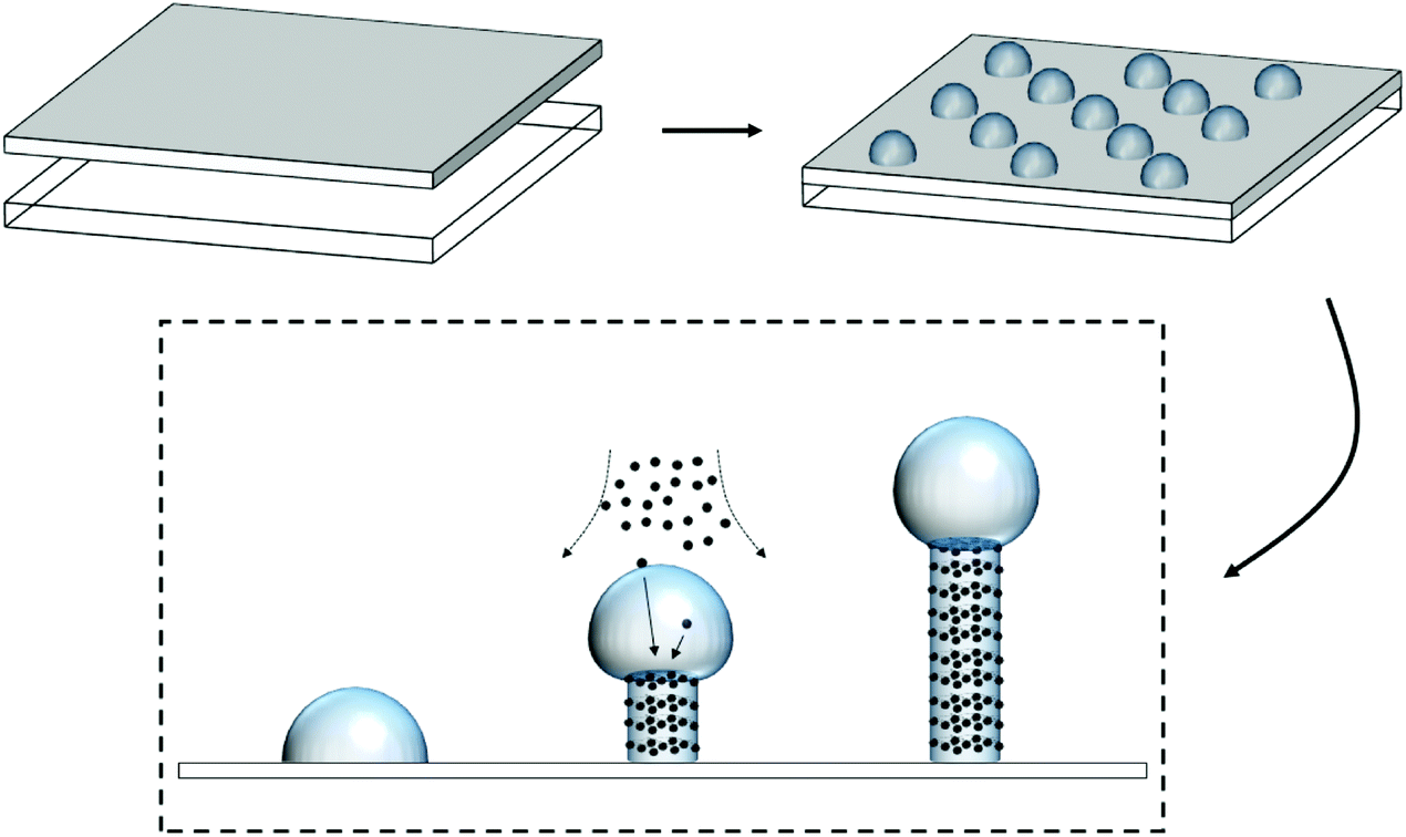 | ||
| Fig. 1 Schematic model of the growth of ITO nanowires by self-catalytic VLS. Several steps are shown: deposition of a uniform thin ITO film of several atomic layers, temperature-driven formation of seeds on the surface as a result of the melting of In–Sn atoms/molecules and growth of nanowires by crystallization of atoms/molecules at the seed–semiconductor interface. | ||
A rather rudimentary yet efficient adherence test was conducted to support the proposed epitaxial growth mechanism. This was initially envisaged as a competing procedure to learn if the nanostructured pristine ITO was able to be drawn from a coating material initially deposited on a separate backing material. The coating material must be strongly adhered to the backing material. As we shall see, the nanostructured ITO draws all the adhesive material, which indicates its high surface area and compatibility with the adhesive. The experiment also provided information on the way the nanowires are adhered to the ITO surface. When a piece of adhesive tape was pressured for 10 s on the nanostructured ITO surface and further released, two possibilities existed: that the nanowires remained on the ITO or that they were transferred to the adhesive backed material. To discern it, both the ITO surface and the detached adhesive tape were observed by SEM to learn the fate of the nanowires. They remained on the ITO surface, which indicates that the nanowires are rooted on the ITO surface and grow from the raw material rather than being deposited already in that shape on the ITO film, confirming the self-catalytic VLS hypothesis by which initial ‘seeds’ lead to fully grown wires (please see Fig. 1). Here, two pressure-sensitive adhesives (PSAs) were used: conventional transparent office sellotape (3M Scotch, US) and black electrical tape (Thorlabs, US). The SEM images in Fig. 2 show how in both cases (Fig. 2a and b for Scotch tape and Fig. 2c and d for electrical tape) not only the nanowires were prevented from being detached from the electrode surface, but the adhesive glues were also transferred to the nanowires. These conclusions are confirmed from the EDX spectra shown as the insets in Fig. 2b and d: the red spectra correspond to the bare ITO nanowires, and the peaks of indium, tin and oxygen can be appreciated, together with the intense peak of the substrate silicon; the green spectra correspond to the glue-covered nanowires, and new intense carbon peaks can be observed. On the other hand, no ITO traces were found on the remaining glue in the PSAs (images not shown). The transfer of the adhesive material from the tape to the nanostructured ITO surface can only be interpreted by either a higher affinity of the adhesive material for the nanostructured ITO due to their hydrophilicity or by a high surface area of the nanowires, or by a combination of both.
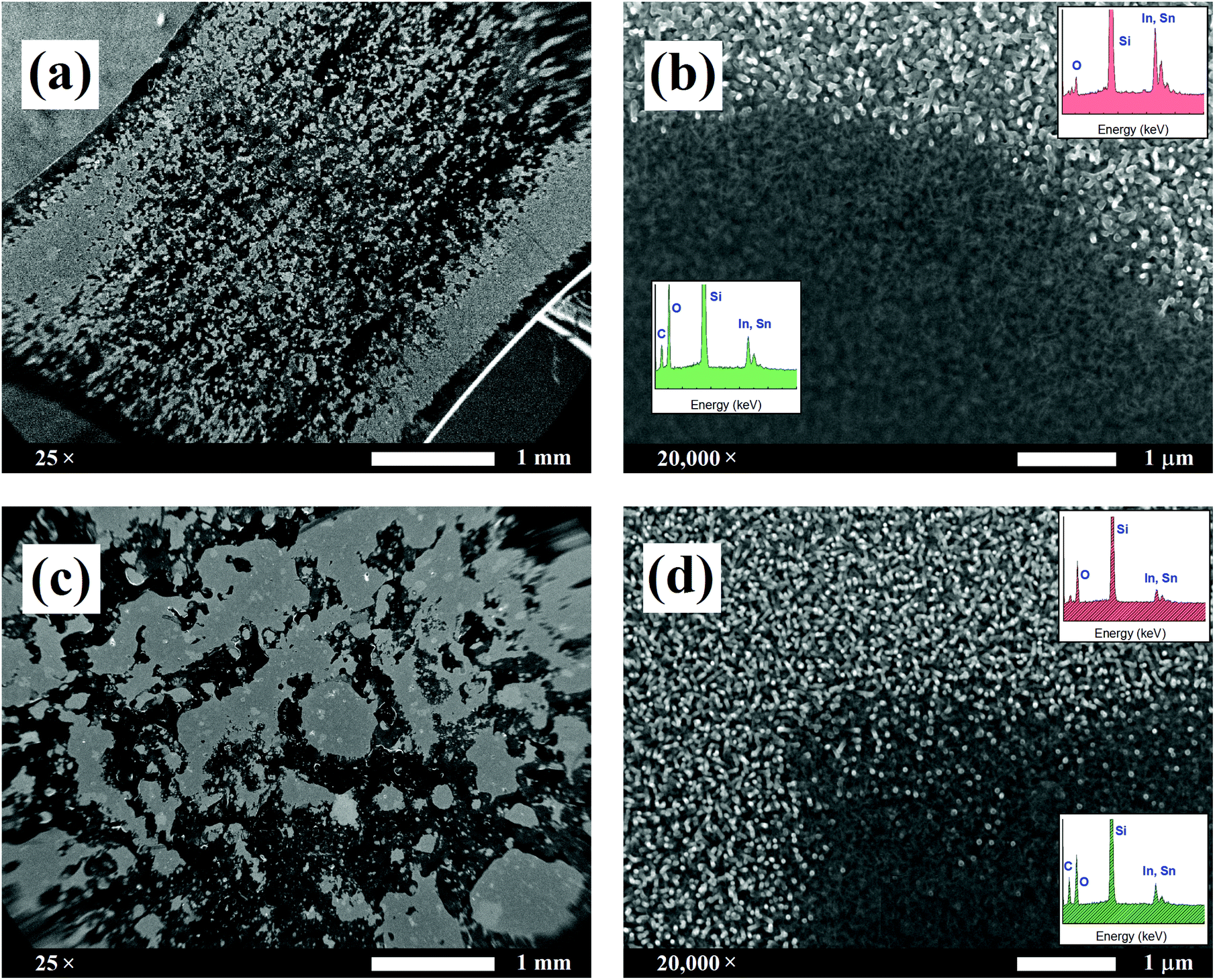 | ||
| Fig. 2 SEM images of nanostructured ITO electrodes pressed for 10 s with (a) and (b) transparent Scotch sellotape, and (c) and (d) black electrical tape. The insets in (b) and (d) contain the EDX spectra of the two distinguishable regions in the SEM images. The red spectra point to the bare ITO nanowires, whereas the green spectra show the carbon peak corresponding to the organic tapes. | ||
3.2 Electro-optical properties
The optical and infrared transmittance spectra for all samples are shown in Fig. 3a. The low optical transparency of the 200 °C sample compared to the rest of the samples can be observed with the naked eye (please see Fig. S3 in the ESI†). Some authors17 ascribe this to an eventual oxygen deficiency in the deposit, suggesting that oxidation of the material is promoted at higher substrate temperatures. The rest of the samples present similar optical transmittance spectra (higher than 80% as deposited). After rapid thermal annealing, the transmittance spectra of all samples converge and skim values around 100% in visible wavelengths. Some studies also report an improvement of transmission properties after plasma treatment of the samples.17,33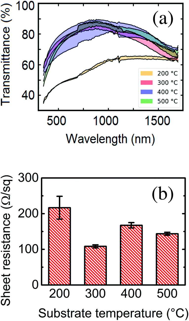 | ||
| Fig. 3 (a) Transmittance spectra (in %) for the as-deposited samples prepared at 200 °C, 300 °C, 400 °C and 500 °C. (b) Sheet resistance (in Ω sq−1) for the samples prepared under the aforementioned conditions. | ||
The reliance of sheet resistance on substrate temperature during deposition is shown in Fig. 3b. A progressive decrease in sheet resistance with increasing growth temperatures can be observed, with a minimum at 300 °C, which could be explained by a change in the final solid phase of the system. Kumar et al.27 presented a slightly shifted yet very similar pattern, which correlated with the atomic percentage of tin in the samples. The sheet resistance values reported in this work stay an order of magnitude below those presented in the cited article (which move around 1 kΩ sq−1). This could be explained by the local differences in the geometry of the nanowires and the thickness of the deposit.
3.3 Faradaic analysis of voltammograms
Cyclic voltammetry in a liquid medium containing a redox probe (Fe(CN)6−3/−4) was used to conduct faradaic electrochemical analysis. The as-recorded cyclic voltammograms of all samples are collected in Fig. S4 in the ESI.† The two-peak motif, typical of single redox-pair systems, can be observed as expected.2,34 The behavior of the faradaic current peaks is described by the Randles–Sevcik equation:35–37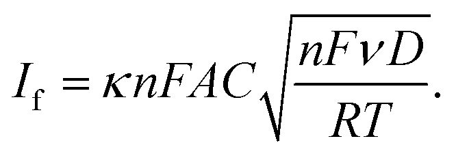 | (1) |
485 C mol−1) and universal gas (8.314 J mol−1 K−1) constants, respectively, A is the electrode area in cm2, ν is the rate at which the potential is swept, in V s−1, D is the analyte's diffusion coefficient in cm2 s−1, C is the analyte's concentration in mol cm−3 and T is the solution temperature in K. This process was thoroughly described elsewhere,2 but briefly, all parameters were known except for the area of the nanostructured electrode. In order to retrieve this area, successive CVs at different scan rates must be performed and the oxidation current against the square rooted scan rate should be plotted. The slope of this plot is directly proportional to the electroactive surface area of the electrode. This, as can be deduced from eqn (1), is only dependent on the electrolyte solution and redox probe composition, providing the electrode is conductive enough. The electrode features are not affecting the intensity of the peak but its position. Indeed, the more resistive the electrode, the wider the separation between reduction and oxidation peaks. This is because redox reactions occur reversibly at the ideal electrode surface, but this reversibility is hindered by the non-ideal conducting properties of the electrode.
The linear dependence of both anodic and cathodic current peak heights (after capacitive current subtraction by EC-Lab software) on the square root of the voltage scan rate (as described in eqn (1)) is shown in Fig. 4a. The highest linearity can be appreciated at low scan rate values, where processes occurring at the electrode–solution interface are quasi-static and quasi-reversible. The results of all linear regressions are summarized in Table 1. As previously stated, the geometrical projected area of the WE in the electrochemical cell is ∼0.3 cm2. Consequently, all samples present evident surface nanostructuration, as observed by SEM, except for the electrode prepared at 200 °C, where nanostructuration is not statistically evident from the numerical data. The sample prepared at 300 °C presents the highest available electroactive surface area. Since the computed surface area seems to correlate with the inverse sheet resistance measured before, the logical question to be asked would be if the effect of surface nanostructuration is being masked by the conductivity of the electrode. Despite that, the theory leading to eqn (1) is built upon the assumption of conductive (metal) electrodes; it is not less true that ITO is considered a transparent conductive electrode yet its applicability in electrochemistry is extensively supported in the literature.38–40 However, let us assume that, given the semi-conductive nature of ITO, the dependence of the measured electrochemically active area on the sheet resistance and eventually on the atomic percentage of tin in the sample is a second order effect. But, from Fig. 3b, the differences in the sheet resistance are within the range of a few ohms, which are hardly observable as a second order effect. On the other hand, the differences in conductivity between samples indeed influence the dependence of the anodic–cathodic peak separation on the preparation substrate temperature of the electrodes, as shown in Fig. 4b. Here, the electrode conductivity indeed plays the role of the first order effect through the entire voltage scan rate range.
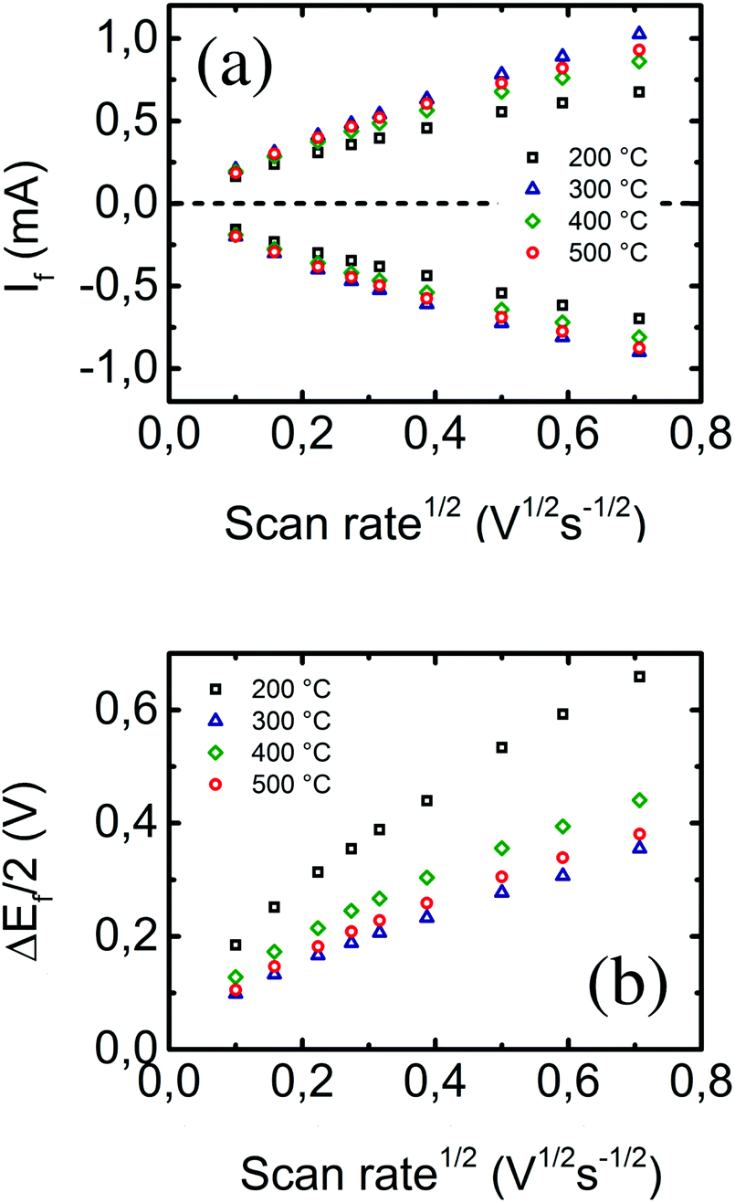 | ||
| Fig. 4 (a) Representation of anodic (upper datasets) and cathodic (lower datasets) faradaic current peaks as a function of the square root of voltage scan rate and (b) dependence of anodic–cathodic voltage peak separation on the square root of voltage scan rate for the as-deposited electrodes prepared at several substrate temperatures. | ||
| Sample | R 2 | a | S.D. | Area |
|---|---|---|---|---|
| 200 °C | 0.993 | 1.38 | 0.06 | 0.31 |
| 300 °C | 0.997 | 1.84 | 0.05 | 0.42 |
| 400 °C | 0.995 | 1.68 | 0.06 | 0.38 |
| 500 °C | 0.998 | 1.77 | 0.04 | 0.40 |
3.4 Non-faradaic analysis of voltammograms
When no redox probe is present in the aqueous medium, interactions at the electrode–solution interface are assumed to be non-faradaic. As there is no redox species, no charge transfer occurs at the electrode surface. Moreover, during cyclic voltammetry, all the current becomes capacitive; no faradaic peaks appear (please see Fig. S5 in the ESI†). In this case, the current height (ideally constant) is proportional to the scan rate, and the differential capacitance becomes the proportionality constant, as shown in the following expression:| Inf = Cd × ν. | (2) |
The differential capacitance is directly proportional to the area of the electrode. This is a faster and more precise method than the classical one for retrieving the electrode's capacitance, which consists of integrating the voltammogram curve and dividing this by the potential scan rate to find the capacitance.41
The cyclic voltammograms of nanostructured ITO films in PBS solution (shown as the dotted line in Fig. 5a), performed at 50 mV s−1, show no remarkable features. The cathodic peak occurs below −0.3 V due to irreversible reduction of the tin oxide,42 eventually causing electrode damage. On the other hand, a current rise would appear around 1 V due to oxygen-related phenomena.43 To avoid these undesirable effects, differential voltammograms (DVs) at the same scan rates were recorded in three narrower potential ranges of width 0.2 V (see solid lines in Fig. 5a). According to some authors,44,45 differences between DV and complete voltammograms occur because of hysteretic phenomena, e.g. slow capacitive processes and charge accumulation. The capacitance for all samples was measured as previously described from the cathodic and anodic current measurements in the three potential ranges. There is now a linear dependence between the anodic and cathodic non-faradaic currents and the voltage scan rate, and the proportionality constant is directly related to the double layer capacitance (see eqn (2)). This is shown in Fig. 5b, from which a clearly differentiated capacitance value can be observed for samples prepared at 300 °C. This is consistent with the fact that this is the sample presenting the highest surface area (retrieved by the faradaic method); assuming that the expression of the parallel-plate capacitor46 can be applied locally in this case, an increase in capacitance is directly explained by an increase in surface area. Specific (per unit area) and mass capacitances for all samples in the three voltage regions (in the region around 0.2 V in the case of mass capacitance) are summarized in Table 2. As predicted by the Mott–Schottky equation47–49 (eqn (3)) for n-type semiconductors, the capacitance decreases with increasing potentials. Further details on this will be analyzed in the following section.
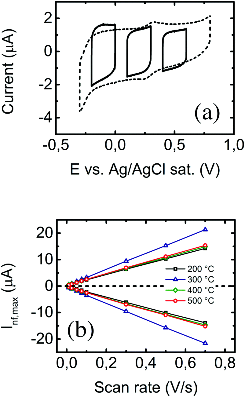 | ||
| Fig. 5 (a) The dashed line corresponds to the non-faradaic CV at 50 mV s−1 of an ITO electrode prepared at 500 °C. The solid lines correspond to the differential voltammograms used to retrieve the double layer capacitance of the samples. (b) Representation of anodic (upper datasets) and cathodic (lower datasets) non-faradaic current values as a function of the potential scan rate for the as-deposited electrodes prepared at several substrate temperatures. | ||
| Sample | Specific capacitance | Mass capacitance | ||
|---|---|---|---|---|
| −100 mV | 200 mV | 500 mV | ||
| 200 °C | 0.993 | 1.38 | 0.06 | 0.31 |
| 300 °C | 0.997 | 1.84 | 0.05 | 0.42 |
| 400 °C | 0.995 | 1.68 | 0.06 | 0.38 |
| 500 °C | 0.998 | 1.77 | 0.04 | 0.40 |
3.5 Proof-of-concept: surface derivatization for biosensing applications
Careful analysis of the results presented in sections 3.3 and 3.4 reveals that the figures of merit obtained from non-faradaic studies are more sensitive to changes in the electrode–solution interface. This may be due to the fact that faradaic processes in semiconductor electrodes become masked by simultaneous non-faradaic ones when capacitive effects are strong. Thereupon, the power of non-faradaic analysis will be used to illustrate the potential use of nanostructured ITO electrodes in biosensing applications, where the quantification of the change in a physicochemical magnitude due to a binding/recognition event at the electrode surface becomes essential. In this section, we will only present the first step of the whole process, which consists of the derivatization of the electrode surface with a layer of molecules (crosslinkers) capable of attaching organic biomolecules (eventually an antibody) to an inorganic substrate (ITO electrode). This insulating crosslinker layer acts as part of the semiconductor electrode in the whole electrochemical system, and thus the physical properties of the electrode become modified. The same would apply to further modification of layers, such as capture antibodies and subsequent antigen detection.In the present work, Mott–Schottky analysis was conducted by recording subsequent electrochemical impedance spectra (EIS) in a limited frequency range and at varying DC voltage polarization values. The AC frequency in the present study ranged from 100 Hz to 10 kHz. This range was chosen after some tests and based on other studies previously reported in the literature.49,50
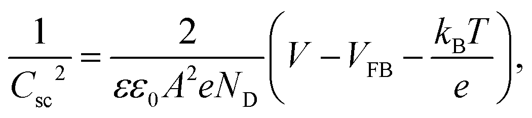
At a determined polarization voltage, the evolution of the charge transfer resistance with subsequent functionalization steps provides qualitative and pseudo-quantitative information on the nature of the insulating layer between the electrode and the solution. On the other hand, the evolution of the electrode capacitance with the polarization voltage accounts for the physical properties of the semiconductor electrode (e.g. the flat band potential of the semiconductor and the density of charge dopants). The latter is gathered in the Mott–Schottky equation, which in turn is derived from Poisson's equation, i.e. the assumption of charge neutrality inside the semiconductor, and Boltzmann's statistics. The Mott–Schottky equation for n-type semiconductor electrodes can be written as47
 | (3) |
Capacitance values can be retrieved by data adjustment of subsequent EIS measurements at several DC polarization voltages in the frequency range of interest. Representation of the measured 1/C2 against DC polarization voltage at a determined frequency value may present several regions with different behaviors.49 Linear fitting of the data points in the region attributable to Csc in eqn (3) eventually leads to the determination of the flat band voltage and carrier density. In this case, the resulting data were fitted to an equivalent circuit consisting of the series association of a resistor (corresponding to the electrolyte solution) and the constant phase element (accounting for the total electrode capacitance), since we are dealing with a non-faradaic system. The total electrode capacitance (Ctot), in turn, consists of the series addition of the double layer capacitance (Cdl, electrode–electrolyte interface) and the semiconductor electrode's internal capacitance (Csc). The latter occurs because of an internal charge distribution due to the external polarization. Since these two capacitances are added serially, Ctot is computed as the inverse of the sum of their reciprocals. Thus, if Csc < Cdl, then Ctot ≈ Csc, and reversely if Cdl < Csc, Ctot ≈ Cdl. These two regimes can be clearly identified in Fig. 6a, where the dependence of the square inverse of the total electrode capacitance against the DC polarization at 100 Hz is plotted for the unmodified ITO electrodes, prepared at the usual substrate temperatures. The lowest region (inside the dotted square) was taken for linear fitting. Fig. 6b shows the evolution of the flat band potentials at 1 kHz for the different electrodes before and after 4-carboxymethyl aryl diazonium (CMA, Sigma Aldrich, Spain) derivatization. Details of the derivatization process are thoroughly described elsewhere.13 In all cases, there is an evolution towards more negative voltage values, which occurs due to a decrease in capacitance: the additional insulating layer (CMA) widens the spatial charge region in the semiconductor electrode (again the parallel-plate capacitor), which means that a larger potential is needed to flatten the electronic bands in the semiconductor. Again, the change in the flat band potential becomes larger in the case of electrodes prepared at a substrate temperature of 300 °C, confirming them as the most sensitive for electrochemical sensing applications.
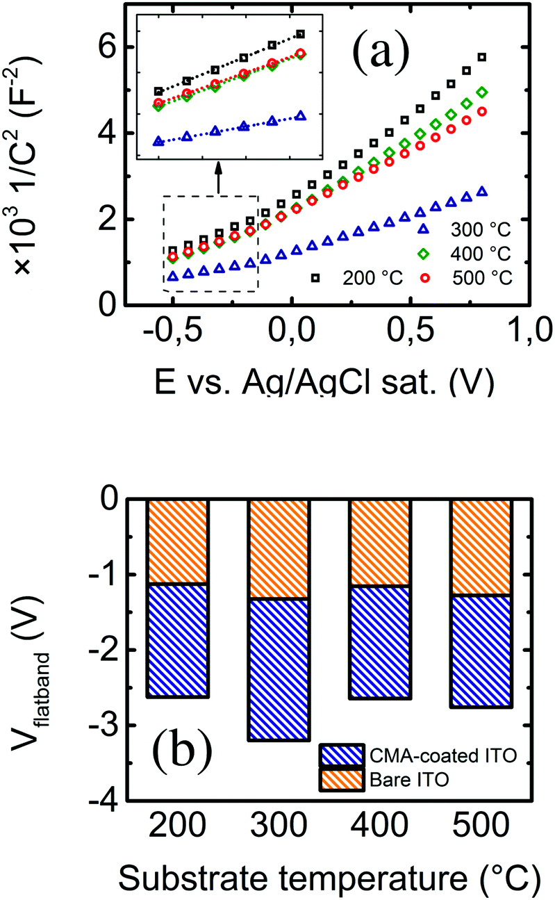 | ||
| Fig. 6 (a) Representation of measured 1/C2vs. DC polarization at 100 Hz, known as Mott–Schottky analysis. Magnification of the linear region at the most negative potentials is shown as the inset, and the subsequent linear regressions correspond to these data points. (b) Bar diagram showing the change in the flat band potential measured by Mott–Schottky analysis at 1 kHz for all samples before (orange) and after (blue) CMA-derivatization of the surfaces. | ||
4 Conclusions
An exhaustive structural and electrochemical analysis of nanostructured ITO electrodes prepared by electron beam evaporation at several substrate temperatures is presented in this work. Some specific conclusions can be drawn:• Self-catalytic VLS growth of ITO nanostructures is promoted by the raise of substrate temperature during deposition, achieving the eutectic point of the SnO2–In2O3 system. Small nanowires are present at a substrate temperature of 200 °C, and the surface area is increased at high temperatures. A controlled Stranski–Krastanov epitaxial growth was achieved by working in a thermodynamic regime and on a crystalline SiO2 substrate. This was proved with a pull-off test, resulting in the adhesive material being transferred to the nanostructured surface, which may be due to the combination of similar hydrophilicity for both materials, a large surface area and the physical attachment of the nanowires to the substrate.
• Faradaic current analysis revealed the highest electrochemical surface area for electrodes prepared at 300 °C. This may be because at 300 °C the separation between nanowires is optimal for redox reactions to reach the electrode surface, whereas (1) at lower temperatures, nanostructuration is not important enough to provide an increased surface area and (2) at higher temperatures, the increased density of whiskers hinders an eventual electron exchange between the solution and the electrode. This implied an increased double layer capacitance for these electrodes, which was confirmed by non-faradaic CV analysis.
• The use of nanostructured ITO electrodes in electrochemical sensing applications was shown by Mott–Schottky analysis of bare and CMA-derivatized electrodes, and those prepared at 300 °C proved to be the most sensitive, as expected. This was useful to characterize the solid-state electronic behavior of n-type semiconductor electrodes, showing that subsequent addition of isolating layers on top of the electrode shifts the flat band potential towards more negative values. The whole analysis is sound with the description of the electronic band diagram of the semiconductor electrode–electrolyte system.
Conflicts of interest
There are no conflicts to declare.Acknowledgements
This work has been funded by the Spanish Ministerio de Economía y Competitividad (CTQ2016-75150-R) and the Generalitat de Catalunya (2014/SGR/149). Centro Nacional de Microelectrónica CNM-CSIC is acknowledged for the technical support. R. P. acknowledges an FPU grant (FPU15/00771) from the Spanish Ministerio de Educación, Cultura y Deporte.References
- A. E. Dixon and J. D. Leslie, Solar Energy Conversion: An Introductory Course, Elsevier, 2013 Search PubMed.
- R. Pruna, F. Palacio, M. López, J. Pérez, M. Mir, O. Blázquez, S. Hernández and B. Garrido, Appl. Phys. Lett., 2016, 109, 063109 CrossRef.
- R. Pruna, F. Palacio, M. Martínez, O. Blázquez, S. Hernández, B. Garrido and M. López, Interface Focus, 2016, 6, 20160056 CrossRef CAS PubMed.
- R. Pruna, F. Palacio and M. López, Multidisciplinary Digital Publishing Institute Proceedings, 2017, p. 288 Search PubMed.
- J. H. Huang, M. H. Hsu, Y. S. Hsiao, P. Chen, P. Yu and C. W. Chu, Sol. Energy Mater. Sol. Cells, 2012, 98, 191–197 CrossRef CAS.
- Y. Y. Kee, S. S. Tan, T. K. Yong, C. H. Nee, S. S. Yap, T. Y. Tou, G. Sfrn, Z. E. Horvth, J. P. Moscatello and Y. K. Yap, Nanotechnology, 2012, 23, 025706 CrossRef PubMed.
- A. Kumar, R. Srivastava, M. N. Kamalasanan and D. S. Mehta, Opt. Lett., 2012, 37, 575–577 CrossRef CAS PubMed.
- C. H. Chiu, P. Yu, C. H. Chang, C. S. Yang, M. H. Hsu, H. C. Kuo and M. A. Tsai, Opt. Express, 2009, 17, 21250–21256 CrossRef CAS PubMed.
- H.-W. Wang, C.-F. Ting, M.-K. Hung, C.-H. Chiou, Y.-L. Liu, Z. Liu, K. R. Ratinac and S. P. Ringer, Nanotechnology, 2009, 20, 055601 CrossRef PubMed.
- G. A. Rivas, M. D. Rubianes, M. C. Rodriguez, N. F. Ferreyra, G. L. Luque, M. L. Pedano, S. A. Miscoria and C. Parrado, Talanta, 2007, 74, 291–307 CrossRef CAS PubMed.
- K. P. S. Dancil, D. P. Greiner and M. J. Sailor, J. Am. Chem. Soc., 1999, 121, 7925–7930 CrossRef CAS.
- N. Yang, H. Zhuang, R. Hoffmann, W. Smirnov, J. Hees, X. Jiang and C. E. Nebel, Anal. Chem., 2011, 83, 5827–5830 CrossRef CAS PubMed.
- R. Pruna, A. Baraket, A. Bonhommé, N. Zine, A. Errachid and M. López, Electrochim. Acta, 2018, 283, 1632–1639 CrossRef CAS.
- C. K. Choi, K. D. Kihm and A. E. English, Opt. Lett., 2007, 32, 1405–1407 CrossRef CAS PubMed.
- C. K. Choi, C. H. Margraves, S. I. Jun, A. E. English, P. D. Rack and K. D. Kihm, Sensors, 2008, 8, 3257–3270 CrossRef CAS PubMed.
- M. Fung, Y. Sun, A. Ng, A. Djurišić and W. Chan, Curr. Appl. Phys., 2011, 11, 594–597 CrossRef.
- J. H. Park, H. K. Park, J. Jeong, W. Kim, B. K. Min and Y. R. Do, J. Electrochem. Soc., 2011, 158, K131 CrossRef CAS.
- N. Wan, J. Xu, G. Chen, X. Gan, S. Guo, L. Xu and K. Chen, Acta Mater., 2010, 58, 3068–3072 CrossRef CAS.
- A. L. Beaudry, R. T. Tucker, J. M. Laforge, M. T. Taschuk and M. J. Brett, Nanotechnology, 2012, 23, 105608 CrossRef CAS PubMed.
- T.-K. Yong, S.-S. Tan, C.-H. Nee, S.-S. Yap, Y.-Y. Kee, G. Sáfrán, Z. Horváth, J. Moscatello, Y.-K. Yap and T.-Y. Tou, Mater. Lett., 2012, 66, 280–281 CrossRef CAS.
- J. G. Van Dijken and M. J. Brett, J. Vac. Sci. Technol., A, 2012, 30, 040606 CrossRef.
- C. O'Dwyer, M. Szachowicz, G. Visimberga, V. Lavayen, S. B. Newcomb and C. M. Torres, Nat. Nanotechnol., 2009, 4, 239–244 CrossRef PubMed.
- H.-S. Jang, D.-H. Kim, H. R. Lee and S.-Y. Lee, Mater. Lett., 2005, 59, 1526–1529 CrossRef CAS.
- K. Kalyanikutty, G. Gundiah, C. Edem, A. Govindaraj and C. Rao, Chem. Phys. Lett., 2005, 408, 389–394 CrossRef CAS.
- A. Irrera, E. F. Pecora and F. Priolo, Nanotechnology, 2009, 20, 135601 CrossRef CAS PubMed.
- P. Artoni, E. F. Pecora, A. Irrera and F. Priolo, Nanoscale Res. Lett., 2011, 6, 162 CrossRef PubMed.
- R. R. Kumar, K. N. Rao, K. Rajanna and A. Phani, Mater. Res. Bull., 2014, 52, 167–176 CrossRef CAS.
- C. E. White, Phase diagrams of indium alloys and their engineering applications, Asm Intl, 1992, vol. 8 Search PubMed.
- N. David, K. El Aissaoui, J. Fiorani, J. Hertz and M. Vilasi, Thermochim. Acta, 2004, 413, 127–137 CrossRef CAS.
- A. Baskaran and P. Smereka, J. Appl. Phys., 2012, 111, 044321 CrossRef.
- Q. Li, F. Yun, Y. Li, W. Ding and Y. Zhang, Sci. Rep., 2017, 7, 1600 CrossRef.
- N. Yamamoto, K. Morisawa, J. Murakami and Y. Nakatani, ECS Solid State Lett., 2014, 3, 84–86 CrossRef.
- C. Lee, Effects of plasma treatment on the electrical and optical properties of indium tin oxide films fabricated by r.f. reactive sputtering, 2001, http://linkinghub.elsevier.com/retrieve/pii/S0040609001007775.
- A. A. Ansari, A. Kaushik, P. R. Solanki and B. D. Malhotra, Electrochem. Commun., 2008, 10, 1246–1249 CrossRef CAS.
- A. J. Bard and L. R. Faulkner, Electrochemical methods: fundamentals and applications, Wiley, New York, 1980, vol. 2 Search PubMed.
- V. Gau, S.-C. Ma, H. Wang, J. Tsukuda, J. Kibler and D. A. Haake, Methods, 2005, 37, 73–83 CrossRef CAS PubMed.
- J. C. Myland and K. B. Oldham, J. Electroanal. Chem., 1983, 153, 43–54 CrossRef CAS.
- M. Mierzwa, E. Lamouroux, I. Vakulko, P. Durand and M. Etienne, Electrochim. Acta, 2016, 202, 55–65 CrossRef CAS.
- A. Deep, S. K. Bhardwaj, A. K. Paul, K. H. Kim and P. Kumar, Biosens. Bioelectron., 2015, 65, 226–231 CrossRef CAS PubMed.
- Y. Lin, Y. Peng and J. Di, Sens. Actuators, B, 2015, 220, 1086–1090 CrossRef CAS.
- A. Allagui, T. J. Freeborn, A. S. Elwakil and B. J. Maundy, Sci. Rep., 2016, 6, 38568 CrossRef CAS PubMed.
- S. Bouden, A. Dahi, F. Hauquier, H. Randriamahazaka and J. Ghilane, Sci. Rep., 2016, 6, 36708 CrossRef CAS PubMed.
- Y. Liu and W. E. Mustain, J. Am. Chem. Soc., 2013, 135, 530–533 CrossRef CAS PubMed.
- Y. Oren and A. Soffer, J. Electroanal. Chem., 1985, 186, 63–77 CrossRef CAS.
- F. Montilla, E. Morallón, A. De Battisti and J. L. Vázquez, J. Phys. Chem. B, 2004, 108, 5036–5043 CrossRef CAS.
- C. Largeot, C. Portet, J. Chmiola, P. L. Taberna, Y. Gogotsi and P. Simon, J. Am. Chem. Soc., 2008, 130, 2730–2731 CrossRef CAS.
- K. Gelderman, L. Lee and S. W. Donne, J. Chem. Educ., 2007, 84, 685 CrossRef CAS.
- K. Rajeshwar, Encyclopedia of Electrochemistry, Wiley-VCH Weinheim, Germany, 2007, pp. 1–53 Search PubMed.
- N. R. Shanmugam, S. Muthukumar, A. P. Selvam and S. Prasad, Nanomedicine, 2016, 11, 1345–1358 CrossRef CAS PubMed.
- O. Almora, C. Aranda, E. Mas-Marzá and G. Garcia-Belmonte, Appl. Phys. Lett., 2016, 109, 173903 CrossRef.
Footnote |
| † Electronic supplementary information (ESI) available: SEM micrographs of the as-deposited ITO films at several temperatures; transparency of the as-deposited ITO electrodes prepared at several temperatures; the as-recorded faradaic and non-faradaic cyclic voltammograms. See DOI: 10.1039/C8NR07908K |
| This journal is © The Royal Society of Chemistry 2019 |