
Neuronal dynamics in HfOx/AlOy-based homeothermic synaptic memristors with low-power and homogeneous resistive switching†
Sungjun
Kim
 a,
Jia
Chen
b,
Ying-Chen
Chen
c,
Min-Hwi
Kim
d,
Hyungjin
Kim
d,
Min-Woo
Kwon
d,
Sungmin
Hwang
d,
Muhammad
Ismail
a,
Yi
Li
b,
Xiang-Shui
Miao
b,
Yao-Feng
Chang
*e and
Byung-Gook
Park
*d
a,
Jia
Chen
b,
Ying-Chen
Chen
c,
Min-Hwi
Kim
d,
Hyungjin
Kim
d,
Min-Woo
Kwon
d,
Sungmin
Hwang
d,
Muhammad
Ismail
a,
Yi
Li
b,
Xiang-Shui
Miao
b,
Yao-Feng
Chang
*e and
Byung-Gook
Park
*d
aSchool of Electronics Engineering, Chungbuk National University, Cheongju 28644, South Korea
bSchool of Optical and Electronic Information & Wuhan National Laboratory for Optoelectronics, Huazhong University of Science and Technology, Wuhan 430074, China
cMicroelectronics Research Center, University of Texas at Austin, Austin, Texas 78758, USA
dInter-university Semiconductor Research Center (ISRC) and the Department of Electrical and Computer Engineering, Seoul National University, Seoul 08826, South Korea. E-mail: bgpark@snu.ac.kr
eIntel Corporation, Hillsboro, USA. E-mail: yfchang@utexas.edu
First published on 27th November 2018
Abstract
We studied the pseudo-homeothermic synaptic behaviors by integrating complimentary metal–oxide–semiconductor-compatible materials (hafnium oxide, aluminum oxide, and silicon substrate). A wide range of temperatures, from 25 °C up to 145 °C, in neuronal dynamics was achieved owing to the homeothermic properties and the possibility of spike-induced synaptic behaviors was demonstrated, both presenting critical milestones for the use of emerging memristor-type neuromorphic computing systems in the near future. Biological synaptic behaviors, such as long-term potentiation, long-term depression, and spike-timing-dependent plasticity, are developed systematically, and comprehensive neural network analysis is used for temperature changes and to conform spike-induced neuronal dynamics, providing a new research regime of neurocomputing for potentially harsh environments to overcome the self-heating issue in neuromorphic chips.
Introduction
A memristor is a nonlinear, passive two-terminal resistance component associated with the combination of charge and magnetic flux, proposed by Leon Chua in 1971,1 the concept of which has been extended into practical applications by HP Labs.2,3 Of the various types of memristor, including phase-change memory (PCRAM),4–6 magnetic memory (MRAM),7 and resistive memory (RRAM),8 RRAM has certain advantages, such as fast switching (∼10 ns),9 low-power operation (∼1 μA),10 and high-density with three-dimensional (3D) vertical structures11–13 from the use of several materials, including metal oxides and nitrides. Although RRAM is reported to have evolved through more than a decade of research,8–32 it is currently insufficient to be used as a stand-alone memory or NAND replacement. Rather, RRAM may be more appropriate for application to storage-class memory (SCM), because of its low read latency and fast writing speed. SCM can shorten the performance gap between NAND and DRAM, and ultimately can be used to form a new memory hierarchy.33 Another important application using RRAM devices is neuromorphic computing, which employs brain-inspired information processing principles to enable artificial intelligence and machine learning.34–46 With the advent of the big data era, it is inefficient to handle large and complex real-time data, such as speech and image recognition, with the existing von Neumann architecture. The brain is made up of 100 billion neurons, each connected to thousands of synapses. The synapses send and receive chemical signals to two adjacent neurons, and the enhancement of synaptic signaling is accepted as a mechanism of learning and memory. The memristor is a two-terminal device that can act like a synapse in the nervous system. That is, the conductance of the device can be gradually changed and maintained in accordance with an externally applied pulse signal.To mimic neuronal activities in a human brain following a homeothermic organism, or even over-performance within various temperature environments similar to poikilotherms, the temperature change in neuronal dynamics needs to be investigated at the memristor synapse, which would help researchers to understand the use of emerging memristor-type neuromorphic computing systems, and to improve their performance through material- and device-level engineering. Although evidence suggests that changes in the brain temperature could have profound effects on neural activity and functions, our knowledge of brain temperature, its normal and pathological fluctuations, and the mechanisms underlying brain thermal homeostasis is very limited. Here, complementary metal–oxide–semiconductor (CMOS) friendly synapse memristors (Ni/HfOx/n++Si) have been explored to imitate the temperature variation in neuronal dynamics. Although the use of silicon bottom electrode tends to increase the operating voltage, the operating current tends to decrease.22 Moreover, a memristor using a silicon substrate as the bottom electrode has the advantage of self-rectifying without an additional selector.46 This characteristic can be applied to the memristor even when operating a synapse array. In this work, potential pseudo-homeothermic synapse activity and neural network functionality was evaluated by recognition accuracy with a wide range of temperature changes in neuronal dynamics and functionality due to the fact that homoeothermic material properties are achieved compared to typical synapse memristors (Ni/HfOx/p++Si). The synaptic behaviors, including long-term potentiation (LTP), long-term depression (LTD), and spike-timing-dependent plasticity (STDP) of HfOx-based RRAM devices, were demonstrated considering various temperature ranges, including the human body temperature. Finally, the influences of temperature and AlOy layer insertion were confirmed through pattern recognition in a neural network simulation.
Experimental
Here, Ni/HfOx/p++Si, Ni/HfOx/n++Si, and Ni/HfOx/AlOy/n++Si memristor devices were fabricated as follows: ion implantation was used to form a high concentration of impurities in Si. For the p++Si and n++Si BEs, BF2+ and P ions, respectively, with a dose of 5 × 1015 cm−2 and at an acceleration energy of 40 keV, were implanted into Si lattices. The annealing process then proceeded at 1050 °C for 10 min to activate the impurities and restore the broken lattices. The sheet resistances were 30.21 Ω sq−1 and 15.55 Ω sq−1 for the p++ and n++ Si Bes, respectively. Then, a HfOx layer with a thickness of 3.5 nm was deposited on the Si BEs using an ALD with tetrakis (ethylmethylamino) hafnium (TEMAH) and ozone (O3) as the precursor. To gain additional information about the low-power memristor characteristics, a 1.5 nm thick AlOy film was deposited on the n++Si BE using ALD by trimethylaluminum (TMA) and O3 for the Ni/HfOx/AlOy/n++Si device. Finally, a 100 nm thick Ni top electrode (TE) with a diameter of 100 μm was deposited on the HfOx layer by thermal evaporation for the three devices. All the electrical properties were characterized by DC voltage sweep and pulse modes, using a Keithley 4200-SCS semiconductor parameter analyzer and 4225-PMU ultrafast I–V module at different temperatures, respectively. For device operation, the Si BEs were grounded and the Ni TE bias were controlled.Results and discussion
Fig. 1a and b show the concept of pseudo-homeothermic-like and -ectothermic-like memristor synapses, respectively. Homeothermic organisms, such as birds and mammals, have evolved autonomic and behavioral thermoeffectors to maintain a relatively constant core temperature over a wide range of environmental temperatures. On the contrary, poikilotherms, such as reptiles, amphibians, fish, and insects, have internal temperatures that vary with the environmental temperature. In general, homeotherms have much higher output performance in terms of behaviors and learning; however, they can only function over a very narrow range of body temperatures as compared to poikilotherms (Fig. 1a). The change in body temperature can be forced or regulated in homeotherms (Fig. 1b). Forced changes in temperature come from the damage of thermoeffector functions for heat gain or loss. However, best performance is observed with a normal set-point (TSET). Forced hyperthermia (Tmax) and hypothermia (Tmin) also occur when the thermoregulatory system is affected by the exposure to the outside environment. However, a regulated change in temperature is controlled when a change in TSET activates thermoeffector responses to the body temperature. The fundamental temperature control in homeothermic organisms by thermoregulation should be considered with respect to neuronal activities and neuronal dynamics, given that small changes of as little as 2–3 °C in brain temperature can affect neuronal behaviors.47 Moreover, it can be shown that in a number of systems, such as in the activation and inactivation of ion channels in neuronal membranes (Fig. 1c), the conduction velocity of action potentials, presynaptic transmitter release, and postsynaptic reception change considerably as the temperature of the nervous system changes. The effects on the neural activity and neural functions of temperature suggest that the pathological fluctuations and mechanisms underlying brain thermal homeostasis are highly related to neuromorphic computing system efficiency.48 Herein, Ni/HfOx/n++Si and Ni/HfOx/AlOy/n++Si memristor devices were used to mimic the temperature change in neuronal dynamics. A transmission electron microscopy (TEM) image of a Ni/HfOx/AlOy/n++Si device, which could imitate biological synaptic functions including a potential pseudo-homeothermic synapse activity, is shown in Fig. 1d. In addition, X-ray photoelectron spectroscopy (XPS) analysis was performed to confirm the composition ratio of the device (ESI, Fig. S1†) to obtain exact composition values. Both layers of HfOx and AlOy showed a non-stoichiometric characteristic of oxygen deficiency. | ||
| Fig. 1 (a) Body temperature as a function of external temperature for a homeotherm and poikilotherm. (b) Energy performance for a homeotherm and poikilotherm. (c) Schematic of biological synapse. (d) TEM image of Ni/HfOx/AlOy/n++Si synaptic device. | ||
Fig. 2a–c show the resistive switching properties of three HfOx-based memristor devices. Two different resistive switching characteristics could be observed from the I–V curves. A Ni/HfOx/p++Si device that exhibits abrupt set and reset switching follows a typical filamentary model, as shown in Fig. 2a. A forming and set process to produce a conducting filament occurs near approximately 3.5 V, and a reset is initiated to rupture the conducting filament around −1 V. On the contrary, the Ni/HfOx/n++Si device exhibits typical interface-type switching, as shown in Fig. 2b. This device has the advantage that there is no need to apply an external current limit. In the literature, filamentary-type and interface-type switching are reported simultaneously in HfOx-based RRAM.49–55Table 1 compares previously reported resistive switching parameters in HfOx-based memristor devices, including filamentary and interface types. HfOx-based RRAM exhibits resistance switching characteristics in various stacks. The switching thickness is 3 nm to 20 nm and the HfOx film deposition method varies, including chemical vapor deposition (CVD), atomic layer deposition (ALD), and sputtering methods. In terms of mass production, electrodes, such as Si and TiN, are preferred over noble metals, such as Pt and Au. CVD- or ALD-based HfOx films are more suitable for high-density 3D stacking.
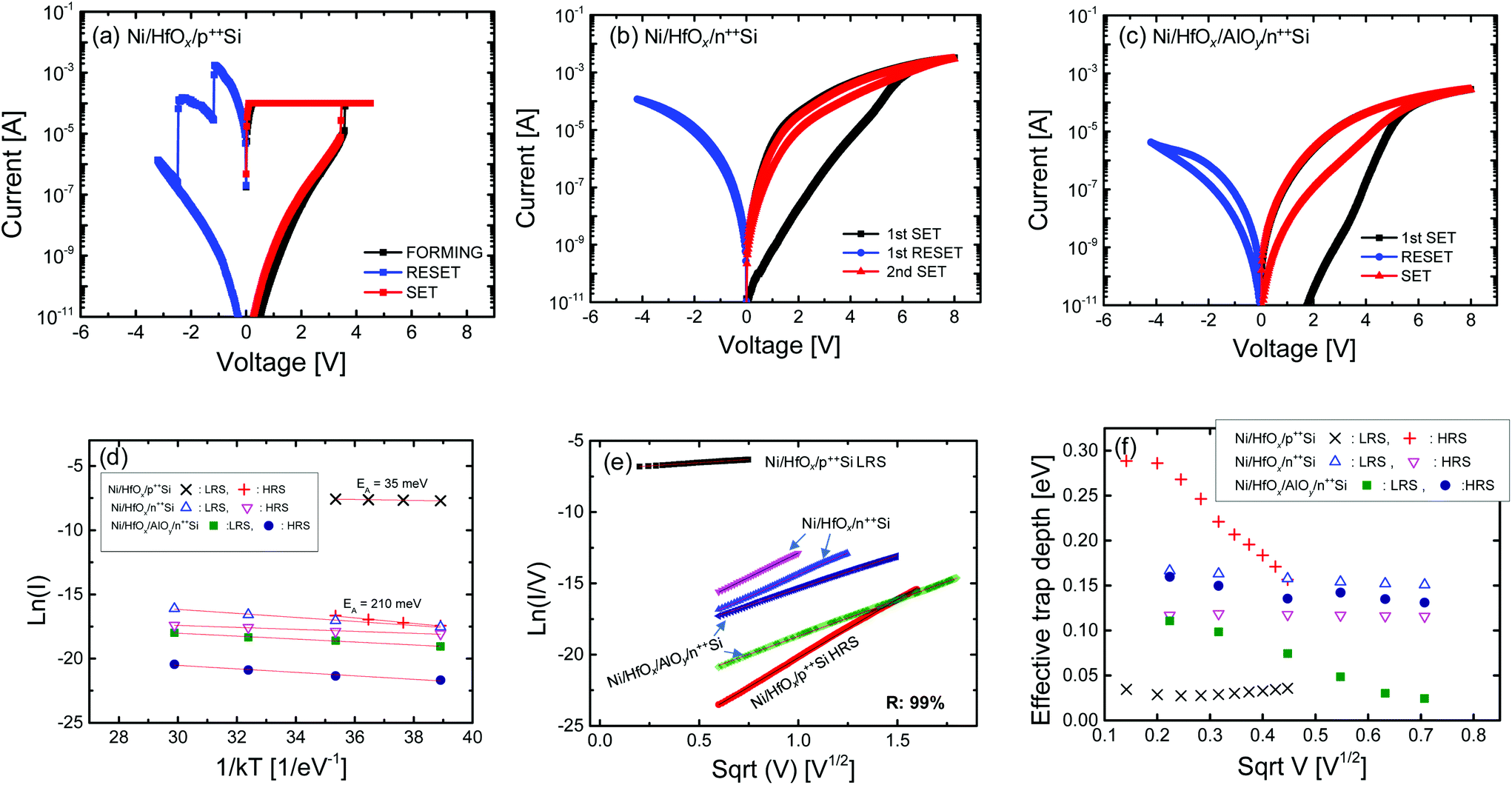 | ||
| Fig. 2 I–V curves at room temperature: (a) Ni/HfOx/p++Si, (b) Ni/HfOx/n++Si, (c) Ni/HfOx/AlOy/n++Si devices. Ln(I) vs. 1/kT for three devices in the LRS and HRS. (d) Ln(I/V) vs. V1/2 for Poole–Frenkel emission. (e) Effective trap depth for three devices in the LRS and HRS. | ||
| Device stack | Deposition method | Switching polarity | Switching type | SET | RESET | RESET current | On/off ratio |
|---|---|---|---|---|---|---|---|
| Ti/HfO2:Al/Pt49 | PVD | Bipolar | Filamentary | Abrupt | Gradual | <3 mA | >20 |
| Ti/HfO2/Al2O3/TiN50 | ALD | Bipolar | Filamentary | Abrupt | Gradual | <200 μA | <100 |
| TiN/HfO2/TiN51 | ALD | Unipolar | Filamentary | Abrupt | Abrupt | <200 μA | <20 |
| Au/HfO2/Pt52 | MOCVD | Unipolar | Filamentary | Abrupt | Abrupt | <50 mA | >104 |
| Al/AlOx/HfOx/Pt53 | ALD | Bipolar | Filamentary | Abrupt | Gradual | <2 mA | <103 |
| Pt/HfOx/TiN54 | RMBE | Bipolar | Interface | Gradual | Gradual | <1 mA | <5 |
| TE/HfOx/SiOy/Si55 | N/A | Bipolar | Interface | Gradual | Gradual | <1 μA | <50 |
| Ni/HfOx/AlOy/n++-Si [This work] | ALD | Bipolar | Interface | Gradual | Gradual | <5 μA | <20 |
HfOx-based RRAM shows both unipolar and bipolar switching. For unipolar switching, the conducting filaments are ruptured by Joule heating with high current at reset switching. However, in bipolar operation, it is possible to rupture the conducting filaments at a lower current, which is induced by the drift of the oxygen vacancies under a low electric field. The filamentary-type switching has a higher low-resistance state (LRS) current and larger on/off ratios than the interface type. Similar to HfOx RRAM, other material systems, such as Ti/TiO2/SiOx/n++Si and Pt/ZnO/Pt devices, have been found to exhibit both filamentary- and interface-type switching.56,57 For synapse applications, a gradual resistance change is essential during set and reset operations. In a set operation, abrupt switching is commonly observed in filamentary types. In this case, it is difficult to implement multiple levels owing to a large change in conductance with the applied voltage. Self-compliance by series resistance can cause multiple conductance jumps to occur. However, in this case, it is also difficult to achieve cycle-to-cycle reproducibility for multi-levels. A progressive set, which is observed in the interface type, is optimized for synaptic devices because it ensures fine-tuning for resistance or conductance states. Reset switching can be also generated in various ways. For the filament type, the conductance essentially changes abruptly or by several step-by-step changes. However, the interface type shows a progressive decrease in the conductance.
Fig. 2c shows the I–V characteristics of a Ni/HfOx/AlOy/n++Si device. The insertion of an Al2O3 layer with a large bandgap (∼9 eV) with insulating properties can lower the LRS and HRS currents.29 In addition, Al2O3, which has a higher dielectric constant (∼9) than SiO2 (3.9), can more effectively eliminate the remaining oxygen vacancies, owing to its higher thermal conductivity, especially for lower HRS current by using a deep reset. It should be noted that this is one of the practical ways to increase the low on/off ratio of interface-type memristors. Fig. 2d shows the current change as a function of temperature in the LRS and HRS for the three devices. The extraction activation energy (EA) of the Ni/HfOx/p++Si device showing the filament type is very different between the LRS (35 meV) and HRS (210 meV). This is associated with the formation of conducting filaments in the LRS, which dominates the main conductance. The increasing current with increasing temperature indicates that the filament has a semiconducting property. We can exclude the intense penetration of strong Ni through HfOx or strong oxygen deficiency inside the HfOx film. Both metallic and semiconducting filaments are reported in the literature for the temperature dependence of LRS. This can be influenced by the current level by compliance or overshoot and the stack combination. However, for Ni/HfOx/n++Si and Ni/HfOx/AlOy/n++Si devices showing interface-type switching, the current change with temperature has a more consistent range (EA: 77–156 meV) regardless of whether the device is in the LRS or HRS. Fig. 3e shows ln(I/V) vs. V1/2 for the three devices in the HRS and LRS to confirm the Poole–Frenkel emission model,58 and to obtain the effective trap depth below the conduction band (CB) through that relationship. The low-voltage region follows the Poole–Frenkel model well, but the tunneling dominates in the high-voltage region. For the interface type, the lower the current is, the longer regime the Poole–Frenkel model is maintained. The fitting results are good in all regimes before the reset occurs, because the LRS current of the Ni/HfOx/p++Si device is high. Fig. 2f shows the effective trap depth depending on the square root of the voltage in the HRS and LRS of the three devices. Here, the value at which the trend line and the y-axis meet is the height of the barrier. It is noted that the LRS and HRS in the interface type show little difference in trap barrier. Unlike the filamentary model, for the interface type, the oxygen vacancies are densely packed on the surface, and only part of the high concentration on the surface is changed by the applied bias.
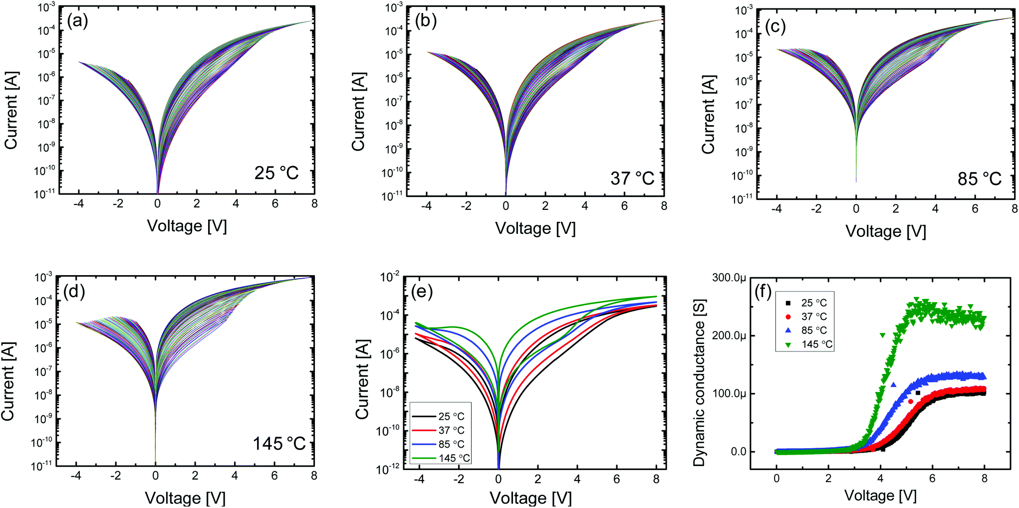 | ||
| Fig. 3 Temperature effects of Ni/HfOx/AlOy/n++Si device: MLC characteristics at different temperatures at (a) 25 °C. (b) 37 °C, (c) 85 °C, (d) 145 °C. (e) I–V characteristics by varying temperature. (f) Dynamic conductance. | ||
To investigate the pseudo-homeothermic biological model applicable to the memristors according to the two different switching types shown above, the temperature dependence in the devices was closely examined. As Ni/HfOx/p++Si exhibits filamentary switching, the reset switching does not occur at high temperature (85 °C). This results in excessive overshoot during the forming process, which makes it difficult to rupture the large conductive filaments upon reset switching (ESI, Fig. S2†). This characteristic is similar to that of a poikilotherm, such as reptiles, that changes its internal temperature characteristics according to the external environment. That is, according to the external voltage, the memristor shows different characteristics. Essentially, the filamentary type exhibits a random distribution with respect to the previous switching history, making it difficult to obtain a specific I–V characteristic depending on the temperature.
Fig. 3a–d show DC I–V characteristics by controlling the set and reset stop voltages at various temperatures (25 °C, 37 °C, 85 °C, and 145 °C) for the Ni/HfOx/AlOy/n++Si devices. The current at the positive voltage shows a larger change than that at the negative voltage. Therefore, when current sensing is performed at a positive voltage, a large amount of conductance can be obtained in a wider range. Also, as the temperature rises, the characteristic showing a gradual current change is maintained, but a larger range of conductance change is induced. Fig. 3e shows the switching operation including set and reset switching at different temperatures (25 °C, 37 °C, 85 °C, and 145 °C) for Ni/HfOx/AlOy/n++Si devices. The LRS current tends to increase with increasing temperature. However, the HRS current does not show a constant tendency depending on the temperature, because a strong reset occurs at high temperature. In addition, the devices can have multiple conductance states because they show a greater resistance change when the set process occurs at higher temperature. This can be confirmed by observing the dynamic conductance, which is the derivative of the DC I–V curve (dI/dV) in Fig. 3f. It is difficult to obtain the I–V characteristic with respect to a consistent temperature for the Ni/HfOx/p++Si device exhibiting the filamentary property, because the scattering is severe during the switching operation. On the other hand, pseudo-homeothermic memristors (Ni/HfOx/n++Si and Ni/HfOx/AlOy/n++Si devices) have the advantage of achieving similar characteristics, irrespective of the external environmental temperature, especially for achieving high synaptic behavior even in harsh environments with high temperatures. The above results show that Ni/HfOx/n++Si (homeothermic memristors) with the interface type tends to conduct using deeper traps than Ni/HfOx/p++Si in the LRS. More changes in the absolute amount of the current in the LRS are not important in homeothermic memristors compared to for the poikilotherm memristors. In the case of poikilotherm-type memristors, nonuniform characteristics with temperature changes are not suitable for application to synaptic devices.
To analyze the synaptic properties of the fabricated HfOx-based memristor devices, consecutive pulses were applied to the three devices. When a pulse of magnitude 4.5 V was applied to the Ni/HfOx/p++Si device showing the filamentary property for 100 μs, the conductance increased sharply and there was no additional increment (ESI, Fig. S3a†). Then, when a −2.5 V/100 μs pulse was applied, the conductance abruptly decreased again and the current decreased gradually when the same additional pulses were applied. This behavior is well matched with the results obtained for the I–V characteristic with a DC sweep. On the contrary, the Ni/HfOx/n++Si device showed a gradual conductance change for a higher pulse amplitude. The conductance increased for 50 identical pulses of 8 V/100 μs and then decreased for a pulse of −5 V/100 μs (ESI, Fig. S3b†). The conductance change was approximately 25% of the initial conductance. For the Ni/HfOx/AlOy/n++Si device, the conductance level was reduced by a factor of 100 or more, suggesting that the operating power can be significantly reduced (Fig. 4a). The change in conductance was larger, but the conductance noise became worse, which was due to a reduction in the conducting defects. It is noted that the linearity of LTP was improved in the AlOy-inserted device. The AlOy with a higher dynamic dielectric constant (∼10) affects the distribution of the voltage across the HfOx layer. This may prevent sudden changes in conductance at the beginning by blocking the concentration of the electric field in the HfOx layer. Next, we investigated the LTP and LTD behaviors with respect to temperature for the Ni/HfOx/n++Si and Ni/HfOx/AlOy/n++Si devices. LTP and LTD were observed for the Ni/HfOx/n++Si device with the higher temperatures of 37 °C, 85 °C, and 145 °C (ESI, Fig. S4a–S4c†). A pulse of the same condition (LTP: 8 V/100 μs, LTD: −5 V/100 μs) was applied at different temperatures. As the temperature increased, the value of the conductance at the starting point increased, as did the degree of change in conductance. Fig. 4b–d show LTP and LTD of the Ni/HfOx/AlOy/n++Si device following the homeothermic model with temperatures of 37 °C, 85 °C, and 145 °C. Even at high temperatures, the synaptic properties at room temperature were maintained.
 | ||
| Fig. 4 LTP and LTD at different temperatures (a) 25 °C, (b) 37 °C, (c) 85 °C, (d) 145 °C for Ni/HfOx/AlOy/n++Si. | ||
Furthermore, to estimate the characteristics of different LTP and LTD with temperature effects working as a pattern recognition network, a three-layer neuron network simulation based on a back-propagation (BP) algorithm with the benchmark of the handwriting (MNIST) dataset was performed. The input layer consisted of 784 neurons, which represented 28 × 28 pixels of each character image from MNIST. The neuron number of the hidden layer was 64, and that of the output layer was 10, which represented the numbers 0–9 (Inset of Fig. 5a). Then, each neuron was connected to every neuron in the next layer through synapses. The experimental LTP and LTD properties of the synaptic devices were used to fit as a function of synaptic weight (W) with respect to the input pulse numbers. During the training process, the feedback error of synaptic weight obtained from the BP algorithm was modulated with the function. Then, the deviation between the output and the ideal signal was minimized, which relied on the linearity and accuracy of the experimental resistance tuning. Fig. 5a shows the recognition rate of the Ni/HfOx/AlOy/n++Si devices for different temperatures. The accuracy of the Ni/HfOx/AlOy/n++Si device was generally substantially higher than that of the Ni/HfOx/n++Si device. Especially, the maximum recognition rate of 90.55% was achieved at 37 °C for the Ni/HfOx/AlOy/n++Si device, and the recognition rate did not decrease significantly even when the temperature increased. It is noted that the effect of AlOy layer insertion was to ensure improved accuracy as well as low-power operation (Fig. 5b). The variation was somewhat related to the current level. We improved the recognition rate by changing the pulse condition for each temperature although the recognition accuracy was not perfect due to the nonlinear nature of the memristor (ESI, Fig. S5†).59 In the Ni/HfOx/AlOy/n++Si device, the current increased as the temperature increased, and the variation decreased, as shown in the inset.
 | ||
| Fig. 5 Neural network simulation: (a) accuracy as a function of epoch for Ni/HfOx/AlOy/n++Si device. (b) Accuracy with different temperatures for Ni/HfOx/AlOy/n++Si devices. | ||
Finally, we demonstrated STDP as the Hebbian learning rule for the Ni/HfOx/AlOy/n++Si device with different temperatures. To implement STDP, it was necessary to fine-tune the time interval of the pre-spike and post-spike, and to adjust the pulse amplitude. The amplitude of the pulse was carefully designed to emulate the pre-spike and post-spike in Fig. 6a. The pulses with smaller amplitude were applied at high temperatures, because it is possible to change the synaptic strength to be larger even if the magnitude of the overlapped pulse is small, as in Fig. 6b. The smaller the difference between the two spike timings, the greater the magnitude of the superimposed pulses applied across the device, leading to a larger conductance change.
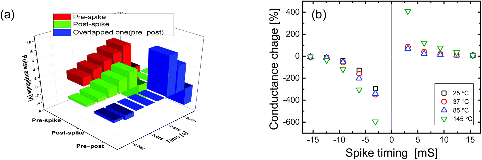 | ||
| Fig. 6 STDP characteristics: (a) pulse scheme for STDP (b) STDP-like curves: conductance change as a function of spike timing. | ||
Conclusions
We fabricated HfOx-based memristor devices using a Si substrate as the lower electrode to analyze pseudo-homeothermic behaviors considering temperature changes, including that of the human body and high temperatures. Ni/HfOx/n++Si devices exhibiting interface switching type are highly suitable for synapse operation by gradually modulating the conductance. We could lower the level of the operating current and obtained more dynamic states by inserting an insulating AlOy layer between the HfOx and n++Si bottom electrode (BE). The neural network simulation showed a more accurate recognition rate in the Ni/HfOx/AlOy/n++Si device, and the recognition rate did not deteriorate significantly even at high temperature operation (∼145 °C). Finally, one of the important biological learning rules, STDP, was demonstrated at various temperatures in the optimized Ni/HfOx/AlOy/n++Si device.Authors contribution
S. Kim prepared the samples and electrical measurements and wrote the manuscript. B.-G. Park and Y.-F. Chang designed the experiments concept. J. Chen did simulation works. J. Chen and Y.-F. Chang wrote manuscript. Y.-C. Chen, M.-H. Kim. H. Kim, M.-W. Kwon, S. Hwang, M. Ismail, Y. Li, X. Miao helped to analysis the experimental results. All authors read and approved the final manuscript.Conflicts of interest
There are no conflicts to declare.Acknowledgements
This work was supported by the National Research Foundation of Korea (NRF) funded by the Korean Ministry of Science, ICT & Future Planning (MSIP) with Grant No. 2018R1A2A1A05023517.Notes and references
- L. O. Chua, IEEE Trans. Circuit Theory, 1971, 18, 507–519, DOI:10.1109/TCT.1971.1083337.
- D. B. Strukov, G. S. Snider, D. R. Stewart and R. S. Williams, Nature, 2008, 453, 80–83, DOI:10.1038/nature06932.
- J. J. Yang, M. D. Pickett, X. Li, D. A. A. Ohlberg, D. R. Stewart and R. S. Williams, Nat. Nanotechnol., 2008, 3, 429–433, DOI:10.1038/nnano.2008.160.
- D.-H. Kang, D.-H. Ahn, K.-B. Kim, J. F. Webb and K.-W. Yi, J. Appl. Phys., 2003, 23, 3536, DOI:10.1063/1.1598272.
- D. Ielmini, A. L. Lacaita and D. Mantegazza, IEEE Trans. Electron Devices, 2007, 54, 308–315, DOI:10.1109/TED.2006.888752.
- Y. Li, Y. Zhong, L. Xu, J. Zhang, X. Xu, H. Sun and X. Miao, Sci. Rep., 2013, 3, 1619, DOI:10.1038/srep01619.
- K. Lee and S. H. Kang, IEEE Trans. Magn., 2011, 47, 131–136, DOI:10.1109/TMAG.2010.2075920.
- R. Waser and M. Aono, Nat. Mater., 2007, 6, 833–840, DOI:10.1038/nmat2023.
- B. Govoreanu, G. S. Kar, Y. Y. Chen, V. Paraschiv, S. Kubicek, A. Fantini, I. P. Radu, L. Goux, S. Clima, R. Degraeve, N. Jossart, O. Richard, T. Vandeweyer, K. Seo, P. Hendrickx, G. Pourtois, H. Bender, L. Altimime, D. J. Wouters, J. A. Kittl and M. Jurczak, Technical Digest - International Electron Devices Meeting, IEDM, 2011. DOI:10.1109/IEDM.2011.6131652.
- H. Y. Lee, Y. S. Chen, P. S. Chen, T. Y. Wu, F. Chen, C. C. Wang, P. J. Tzeng, M. J. Tsai and C. Lien, IEEE Electron Device Lett., 2010, 31, 44–46, DOI:10.1109/LED.2009.2034670.
- B. Gao, Y. Bi, H. Y. Chen, R. Liu, P. Huang, B. Chen, L. Liu, X. Liu, S. Yu, H. S. P. Wong and J. Kang, ACS Nano, 2014, 8, 6998–7004, DOI:10.1021/nn501824r.
- S. Chakrabarti, S. Maikap, S. Samanta, S. Jana, A. Roy and J.-T. Qiu, Phys. Chem. Chem. Phys., 2017, 19, 25938–25948 RSC.
- I. T. Wang, C. C. Chang, L. W. Chiu, T. Chou and T. H. Hou, Nanotechnology, 2016, 27, 365204, DOI:10.1088/0957–4484/27/36/365204.
- M. R. Park, Y. Abbas, H. Abbas, Q. Hu, T. S. Lee, Y. J. Choi, T. S. Yoon, H. H. Lee and C. J. Kang, Microelectron. Eng., 2016, 159, 190–197, DOI:10.1016/j.mee.2016.03.043.
- B. Ku, Y. Abbas, A. S. Sokolov and C. Choi, J. Alloys Compd., 2017, 735, 1181–1188, DOI:10.1016/j.jallcom.2017.11.267.
- H.-D. Kim, M. Yun and S. Kim, J. Alloys Compd., 2015, 651, 340–343, DOI:10.1016/j.jallcom.2015.08.082.
- Y. Yang and W. Lu, Nanoscale, 2013, 5, 10076–10092 RSC.
- S. Gao, F. Zeng, F. Li, M. Wang, H. Mao, G. Wang, C. Song and F. Pan, Nanoscale, 2015, 7, 6031–6038, 10.1039/c4nr06406b.
- Z. Wang, J. Kang, Z. Yu, Y. Fang, Y. Ling, Y. Cai, R. Huang and Y. Wang, Nanotechnology, 2017, 28, 055204 CrossRef PubMed.
- Y. F. Chang, B. Fowler, Y. C. Chen, Y. T. Chen, Y. Wang, F. Xue, F. Zhou and J. C. Lee, J. Appl. Phys., 2014, 116, 043708, DOI:10.1063/1.4891242.
- Y. F. Chang, P. Y. Chen, Y. T. Chen, F. Xue, Y. Wang, F. Zhou, B. Fowler and J. C. Lee, Appl. Phys. Lett., 2012, 101, 05211, DOI:10.1063/1.4742894.
- H. D. Kim, M. J. Yun and S. Kim, J. Alloys Compd., 2015, 653, 534–538, DOI:10.1016/j.jallcom.2015.09.076.
- A. Sawa, Mater. Today, 2008, 11, 28–36 CrossRef CAS.
- S. Long, C. Cagli, D. Ielmini, M. Liu and J. Suñé, IEEE Electron Device Lett., 2011, 32, 1570–1572, DOI:10.1109/LED.2011.2163613.
- K.-C. Chang, T.-C. Chang, T.-M. Tsai, R. Zhang, Y.-C. Hung, Y.-E. Syu, Y.-F. Chang, M.-C. Chen, T.-J. Chu, H.-L. Chen, C.-H. Pan, C.-C. Shih, J.-C. Zheng and S. M. Sze, Nanoscale Res. Lett., 2015, 10, 120 CrossRef PubMed.
- C. C. Hsieh, A. Roy, Y. F. Chang, D. Shahrjerdi and S. K. Banerjee, Appl. Phys. Lett., 2015, 109, 223501, DOI:10.1063/1.4971188.
- A. Mehonic, S. Cueff, M. I. Wojdak, S. Hudziak, O. Jambois, C. Labbé, B. Garrido, R. Rizk and A. J. Kenyon, J. Appl. Phys., 2012, 111, 074507 CrossRef.
- Y. Bai, H. Wu, Y. Zhang, M. Wu, J. Zhang, N. Deng, H. Qian and Z. Yu, Appl. Phys. Lett., 2013, 102, 173503, DOI:10.1063/1.4803462.
- Y.-C. Chen, Y.-F. Chang, X. Wu, F. Zhou, M. Guo, C.-Y. Lin, C.-C. Hsieh, B. Fowler, T.-C. Chang and J. C. Lee, RSC Adv., 2017, 7, 12984–12989 RSC.
- S. Kim, S. Jung, M.-H. Kim, Y.-C. Chen, Y.-F. Chang, K.-C. Ryoo, S. Cho, J.-H. Lee and B.-G. Park, Small, 2018, 14, 1704062, DOI:10.1002/smll.201704062.
- S. Kim and B. G. Park, Appl. Phys. Lett., 2016, 108, 212103, DOI:10.1063/1.4952719.
- S. H. Jo, T. Chang, I. Ebong, B. B. Bhadviya, P. Mazumder and W. Lu, Nano Lett., 2010, 10, 1297–1301, DOI:10.1021/nl904092h.
- S. W. Fong, C. M. Neumann and H.-S. P. Wong, IEEE Trans. Electron Devices, 2017, 64, 4374–4385, DOI:10.1109/TED.2017.2746342.
- Z. Wang, M. Yin, T. Zhang, Y. Cai, Y. Wang, Y. Yang and R. Huang, Nanoscale, 2016, 8, 14015–14022, 10.1039/c6nr00476h.
- S. Li, F. Zeng, C. Chen, H. Liu, G. Tang, S. Gao, C. Song, Y. Lin, F. Pan and D. Guo, J. Mater. Chem. C, 2013, 1, 5292–5298, 10.1039/c3tc30575a.
- Y. Matveyev, K. Egorov, A. Markeev and A. Zenkevich, J. Appl. Phys., 2015, 117, 044901, DOI:10.1063/1.4905792.
- K. Seo, I. Kim, S. Jung, M. Jo, S. Park, J. Park, J. Shin, K. P. Biju, J. Kong, K. Lee, B. Lee and H. Hwang, Nanotechnology, 2011, 22, 254023, DOI:10.1088/0957-4484/22/25/254023.
- Y. F. Chang, B. Fowler, Y. C. Chen, F. Zhou, C. H. Pan, T. C. Chang and J. C. Lee, Sci. Rep., 2016, 6, 21268, DOI:10.1038/srep21268.
- S. Kim, H. Kim, S. Hwang, M. H. Kim, Y. F. Chang and B. G. Park, ACS Appl. Mater. Interfaces, 2017, 9, 40420–40427, DOI:10.1021/acsami.7b11191.
- T. Ohno, T. Hasegawa, T. Tsuruoka, K. Terabe, J. K. Gimzewski and M. Aono, Nat. Mater., 2011, 10, 591–595, DOI:10.1038/nmat3054.
- T. Chang, S. H. Jo and W. Lu, ACS Nano, 2011, 5, 7669–7676, DOI:10.1021/nn202983n.
- S. Yu, Y. Wu, R. Jeyasingh, D. Kuzum and H. S. P. Wong, IEEE Trans. Electron Devices, 2011, 58, 2729–2737, DOI:10.1109/TED.2011.2147791.
- D. S. Jeong, R. Thomas, R. S. Katiyar, J. F. Scott, H. Kohlstedt, A. Petraru and C. S. Hwang, Rep. Prog. Phys., 2012, 75, 076502 CrossRef PubMed.
- D. S. Jeong, K. M. Kim, S. Kim, B. J. Choi and C. S. Hwang, Adv. Electron. Mater., 2016, 2, 1600090 CrossRef.
- Y. V. Pershin and M. Di Ventra, Neural Networks, 2010, 23, 881–886, DOI:10.1016/j.neunet.2010.05.001.
- P. Huang, S. Chen, Y. Zhao, B. chen, B. Gao, L. Liu, Y. Chen, Z. Zhang, W. Bu, X. Liu and J. Kang, IEEE Trans. Electron Devices, 2016, 63, 4295–4310 CAS.
- A. L. Hodgkin and B. Katz, J. Physiol., 1949, 109, 240–249, DOI:10.1113/jphysiol.1949.sp004388.
- J. C. Montgomery and J. A. Macdonald, Am. J. Physiol., 1990, 259, R191–R196, DOI:10.1152/ajpregu.1990.259.2.R191.
- Y. S. Chen, B. Chen, B. Gao, L. F. Liu, X. Y. Liu and J. F. Kang, J. Appl. Phys., 2013, 113, 164507, DOI:10.1063/1.4803076.
- F. De Stefano, M. Houssa, J. A. Kittl, M. Jurczak, V. V. Afanas and A. Stesmans, Appl. Phys. Lett., 2012, 100, 142102, DOI:10.1063/1.3696672.
- U. Chand, K. C. Huang, C. Y. Huang and T. Y. Tseng, IEEE Trans. Electron Devices, 2015, 62, 3665–3670, DOI:10.1109/TED.2015.2471835.
- S. Lee, W.-G. Kim, S.-W. Rhee and K. Yong, J. Electrochem. Soc., 2008, 155, H92–H96, DOI:10.1149/1.2814153.
- M. Akbari, M. K. Kim, D. Kim and J. S. Lee, RSC Adv., 2017, 7, 16704–11678, 10.1039/c6ra26872b.
- S. U. Sharath, J. Kurian, P. Komissinskiy, E. Hildebrandt, T. Bertaud, C. Walczyk, P. Calka, T. Schroeder and L. Alff, Appl. Phys. Lett., 2014, 105, 073505, DOI:10.1063/1.4893605.
- W. Wu, H. Wu, B. Gao, N. Deng, S. Yu and H. Qian, IEEE Electron Device Lett., 2017, 38, 1019–1022, DOI:10.1109/LED.2017.2719161.
- N. Xiao, M. A. Villena, B. Yuan, S. Chen, B. Wang, M. Eliáš, Y. Shi, F. Hui, X. Jing, A. Scheuermann, K. Tang, P. C. McIntyre and M. Lanza, Adv. Funct. Mater., 2017, 27, 1700384, DOI:10.1002/adfm.201700384.
- C. H. Huang, J. S. Huang, C. C. Lai, H. W. Huang, S. J. Lin and Y. L. Chueh, ACS Appl. Mater. Interfaces, 2013, 5, 6017, DOI:10.1021/am4007287.
- Y. F. Chang, B. Fowler, Y. C. Chen, Y. T. Chen, Y. Wang, F. Xue, F. Zhou and J. C. Lee, J. Appl. Phys., 2014, 116, 043709, DOI:10.1063/1.4891244.
- J. H. Bae, S. Lim, B. G. Park and J. H. Lee, IEEE Electron Device Lett., 2017, 38, 1153–1156, DOI:10.1109/LED.2017.2713460.
Footnote |
| † Electronic supplementary information (ESI) available. See DOI: 10.1039/c8nr06694a |
| This journal is © The Royal Society of Chemistry 2019 |