
Anisotropic nonvolatile magnetization controlled by electric field in amorphous SmCo thin films grown on (011)-cut PMN-PT substrates†
Wenhui
Liang
ab,
Fengxia
Hu
 *abc,
Jian
Zhang
*d,
Hao
Kuang
ab,
Jia
Li
ab,
Jiefu
Xiong
ab,
Kaiming
Qiao
ab,
Jing
Wang
*abe,
Jirong
Sun
abc and
Baogen
Shen
abc
*abc,
Jian
Zhang
*d,
Hao
Kuang
ab,
Jia
Li
ab,
Jiefu
Xiong
ab,
Kaiming
Qiao
ab,
Jing
Wang
*abe,
Jirong
Sun
abc and
Baogen
Shen
abc
aBeijing National Laboratory for Condensed Matter Physics and State Key Laboratory of Magnetism, Institute of Physics, Chinese Academy of Sciences, Beijing 100190, China. E-mail: fxhu@iphy.ac.cn; wangjing@iphy.ac.cn
bSchool of Physical Sciences, University of Chinese Academy of Sciences, Beijing 100190, China
cSongshan Lake Materials Laboratory, Dongguan, Guangdong 523808, P. R. China
dKey Laboratory of Magnetic Materials and Devices, Ningbo Institute of Materials Technology and Engineering, Chinese Academy of Sciences, Ningbo 315201, China. E-mail: zhangj@nimte.ac.cn
eFujian Institute of Innovation, Chinese Academy of Sciences, Fuzhou, Fujian 350108, P. R. China
First published on 23rd November 2018
Abstract
The tunable, nonvolatile electrical modulation of magnetization at room temperature is firstly demonstrated in a magnetically hard amorphous SmCo film grown on a (011)-cut 0.7Pb(Mg1/3Nb2/3)O3-0.3PbTiO3 (PMN-PT) substrate. Uniaxial in-plane anisotropy with hard and easy axes lying in the [100] and [01−1] directions, respectively, occurs. Bipolar electric field, E, across the thickness direction enhances the remnant magnetization, Mr, along the hard axis, while suppresses the Mr along the easy axis, and the maximal regulation is about −5.8% and +2.2%, respectively. Detailed analysis indicates that the induced effective uniaxial magnetic anisotropy field, which arises from the magnetostrictive properties of the amorphous SmCo thin film and the anisotropic strain from the PMN-PT substrate, is mainly responsible for the anisotropic tunability. The variation of the directional pair ordering of the SmCo film, which is caused by the anisotropic strain due to the electric field, also contributes to the tunability. More importantly, nonvolatile modulation and a stable two-state memory effect are demonstrated for the bipolar case, and in situ X-ray diffraction and X-ray diffraction reciprocal space mapping reveal that these phenomena originate from the electric-field-induced rhombohedral-orthorhombic phase transformation in the PMN-PT substrate. Moreover, by unipolarizing the ferroelectric substrate, a nonvolatile modulation is also observed. The anisotropic nonvolatile control of magnetization in SmCo amorphous films opens a new avenue for developing multifunctional information storage and novel spintronics devices based on hard magnetic materials.
1. Introduction
Electric field control of magnetism is promising for developing dense, fast, nonvolatile magnetic random access memory (MRAM) with very low energy consumption.1,2 Multiferroic materials with two or more ferroic properties, such as ferroelectricity, ferroelasticity and ferromagnetism/ferrimagnetism,3–9 are strong candidates for achieving the electrical modulation of magnetization, which is induced by the magnetoelectric (ME) effect. The ME effect has attracted such intense interest because of its high speed, low power consumption and high efficiency,10,11 which makes it suitable for potential applications in sensors, multistate memory and other new multifunctional devices.5,12–14 In general, multiferroic materials can be categorised as single-phase multiferroics or multiferroic heterostructures, depending on their composition. Although single-phase multiferroics possess both magnetism and ferroelectricity, their practical applications are limited due to the small ME effect and low working temperature.15 Conversely, multiferroic heterostructures, consisting of ferromagnetic (FM) and ferroelectric (FE) materials, provide a better choice. Based on the origin, the ME effect in the multiferroic heterostructures can be separated into three approaches: strain-mediated coupling,16–21 exchange-bias mediated coupling22,23 and manipulation of charge carrier density.24–26 The most widely studied approach is strain-mediated coupling in FM/FE heterostructures due to the variety of FE and FM materials at room temperature and the remarkable converse ME effects.1,18,27–31 In strain-mediated FM/FE heterostructures, large electric field control of magnetization has been achieved in Fe3O4/PZN-PT(011),18 Ni/BaTiO3![[thin space (1/6-em)]](https://www.rsc.org/images/entities/char_2009.gif) 32 and other systems.29,30,33 However, for most systems, removing the electric field would lead to the piezostrain disappearing, and this volatility in the change of magnetization is problematic for practical applications. Later on, a nonvolatile electric field control of magnetization at room temperature was observed in a number of systems, such as Co40Fe40B20/PMN-PT(001) heterostructures.2 However, the small coverage (26%) of the 109° ferroelastic switching in the entire poled area,34 which plays a major role in the nonvolatile modulation due to its main contribution to the in-plane lattice strain, may lead to inhomogeneity in the regulation.35
32 and other systems.29,30,33 However, for most systems, removing the electric field would lead to the piezostrain disappearing, and this volatility in the change of magnetization is problematic for practical applications. Later on, a nonvolatile electric field control of magnetization at room temperature was observed in a number of systems, such as Co40Fe40B20/PMN-PT(001) heterostructures.2 However, the small coverage (26%) of the 109° ferroelastic switching in the entire poled area,34 which plays a major role in the nonvolatile modulation due to its main contribution to the in-plane lattice strain, may lead to inhomogeneity in the regulation.35
Moreover, in most previous studies, soft FM or ferrimagnetic materials were usually chosen as the FM layer in the FM/FE heterostructures.2,28,30,36–38 To meet the rapidly growing need for developing multifunctional devices, particularly multifunctional information storage devices, the combination of the ME effect and hard magnetic properties is highly desirable. Our recent research indicated that permanent magnetic materials acting as the FM layer, namely Nd2Fe14B thin films,39 can also exhibit the ME effect, demonstrating the possibility of exploring multifunctional devices combining permanent magnetic properties and the ME effect. Nevertheless, it is the spin reorientation in the Nd2Fe14B thin films that can be rotated by an electric field across piezoelectric substrates, and the phenomenon of spin reorientation is not a universal property in permanent magnetic materials. Therefore, nonvolatile electric-field-controlled magnetization in other hard magnetic materials is desirable.
SmCo alloy, a kind of mature and time-honored hard magnetic material, is widely used in daily production and life. Although amorphous SmCo is less popular than crystalline alloys, it is a valuable material that is still studied. Specifically, amorphous SmCo5 films with uniaxial in-plane anisotropy have great potential for applications in information storage and spintronics.40–42 The high recording density and signal-to-noise ratio,40 caused by the high coercivity, the lack of grain boundaries and the smoothness of the film surface, make magnetically hard amorphous SmCo films promising for information storage media.43 The tunable giant magnetic anisotropy,44 magnetic domains,45 the magnetostrictive properties,46 the proximity effects47 and other properties48,49 of amorphous SmCo have been investigated extensively. These studies focus on the suitability of amorphous SmCo thin films for magnetic heterostructures, such as magnetic tunnel junctions,44 the potential application in magnetic memory and magnetic logic circuits,45 the exploration of magnetic anisotropy in amorphous films46 and further clarification of the magnetic proximity effects.47 As known, the mechanism that produces a reversible and permanent magnetic anisotropy change is necessary for electrically writing nonvolatile bit information for MRAM applications.28 Hence, the anisotropy change in amorphous SmCo under electric fields is important for MRAM applications. The strain effect provided by the FE PMN-PT can change the anisotropy, which allows higher storage capacity and lower consumption than voltage-controlled memory devices.50 The combination of the two properties would pave the way for new applications of amorphous SmCo. However, the converse ME effect of thin films grown on piezoelectric substrates has not yet been examined.
In this paper, we report the electrical modulation of magnetization in an amorphous SmCo film grown on a (011)-cut PMN-PT substrate. Uniaxial in-plane anisotropy was established by the in-plane anisotropic strain caused by the substrate. The coercivity (Hc ∼650 Oe) is among the highest reported for magnetically hard amorphous SmCo films.43,44,51–53 Anisotropic nonvolatile electrical modulation of magnetization was demonstrated at room temperature. The results indicate that the poled electric field across the thickness direction increases the remnant magnetization, Mr, in the [100] direction (hard axis) and decreases Mr in the [01−1] direction (easy axis). Detailed analysis indicates that the induced effective uniaxial magnetic anisotropy fields exert the main effect, which blocks the magnetization process along the easy axis and facilitates the magnetization process along the hard axis. The variation of directional pair ordering of the SmCo film caused by the anisotropic strain also contributes to the tunability. The composition of the substrate we chose is around the morphotropic phase boundary (MPB). An irreversible rhombohedral-orthorhombic (R–O) phase transformation was observed by in situ X-ray diffraction and X-ray diffraction reciprocal space mapping (XRD-RSM) of the bipolar state of the substrate, which is responsible for the nonvolatile modulation of magnetic properties for both the hard and easy axis directions. The present work contributes to the area of electric field control of magnetization in FM/FE multiferroic heterostructures, which, in particular, is a substantial step toward realizing electric-field-controlled magnetization in hard magnetic materials, and broadens the potential applications of amorphous SmCo films, such as in electrically writing nonvolatile high-density magnetic memory and in novel multifunctional sensors.
2. Experimental
An amorphous SmCo thin film with a thickness of 50 nm was grown on a (011)-cut PMN-PT substrate by magnetron sputtering in an ultra-high vacuum chamber with a base pressure below 10−6 Pa. A Cr (50 nm) cover layer was deposited at room temperature to prevent oxidation. An Au layer was deposited on the bottom side of the FM/FE structure as electrode. The magnetic properties and their modulation by the electric field were measured by using a Quantum Design superconducting quantum interference device (SQUID VSM) with in situ electric fields provided by an electrometer (6517B, Keithly). X-ray diffraction and XRD-RSM with in situ application of an electric field was performed with a four-circle diffractometer (AXS D8-Discover, Bruker) to identify the structural evolution of the PMN-PT substrate. The polarization-electric field (P-E) curve of PMN-PT was measured in the capacitance configuration using a Radiant FE tester (Premier II). The in-plane strains of PMN-PT induced by the electric bias were measured using a high-resolution strain gauge bonded to the substrate. The width of the pulsed electric field was about 165 s during the repeated Mr pulse measurements.3. Results and discussion
The configuration of the SmCo/(011)PMN-PT heterostructure is shown in Fig. 1(a). To apply an electric field across the PMN-PT substrate, an Au layer was deposited by sputtering as the bottom electrode and the Cr cover layer acted as the top electrode. The commercial (011)-oriented slab of PMN-PT single crystal was chosen as the substrate because it has an excellent anisotropic converse piezoelectric effect. An electric field along the out-of-plane [011] crystalline direction can produce a strong in-plane anisotropic piezostrain in the PMN-PT substrate.54 The left figure in Fig. 1(b) shows the unpoled rhombohedral PMN-PT(011) substrate with eight possible 〈111〉 polarization directions. When a negative electric field is applied along the [0−1−1] direction of the PMN-PT(011) substrate, all of the eight possible polarization directions are switched into two crystal variants, namely the [−1−1−1] and [1−1−1] variants, as shown in the middle figure of Fig. 1(b). On the contrary, when the PMN-PT(011) substrate is poled by a positive electric field, the preferential polarization directions are [111] and [−111] variants. In addition, when the electric field is reversed from one polar to the other, and the electric field is just at the coercive field, the preferential polarization directions are the four possible in-plane 〈111〉 directions, which means that the polarizations undergo a reorientation by non-180° (71° or 109°) polarization switching.28 A schematic of non-180°/180° polarization switching is given in Fig. S1 (ESI†). In this type of polarization, when the substrate is poled along the [011] or [0−1−1] direction, the preferential polarization directions will be above or under the (011) plane. In these cases, the length along the in-plane [100] direction will shrink, and the length along the [01−1] direction will elongate because of the constant volume, and all the [−111] and [111] or [1−1−1] and [−1−1−1] variants tend to be closer to the poled direction.10,55 Moreover, for PMN-PT with composition near the MPB, a structural transformation from the rhombohedral (R) to orthorhombic (O) phase is favored when the poled electric field along [0−1−1] is big enough, and the variants along [1−1−1] and [−1−1−1] are rotated along the [0−1−1] direction,10,55 as shown on the right of Fig. 1(b). As a result, the constriction along the in-plane [100] direction and the extension along the [01−1] direction both increase.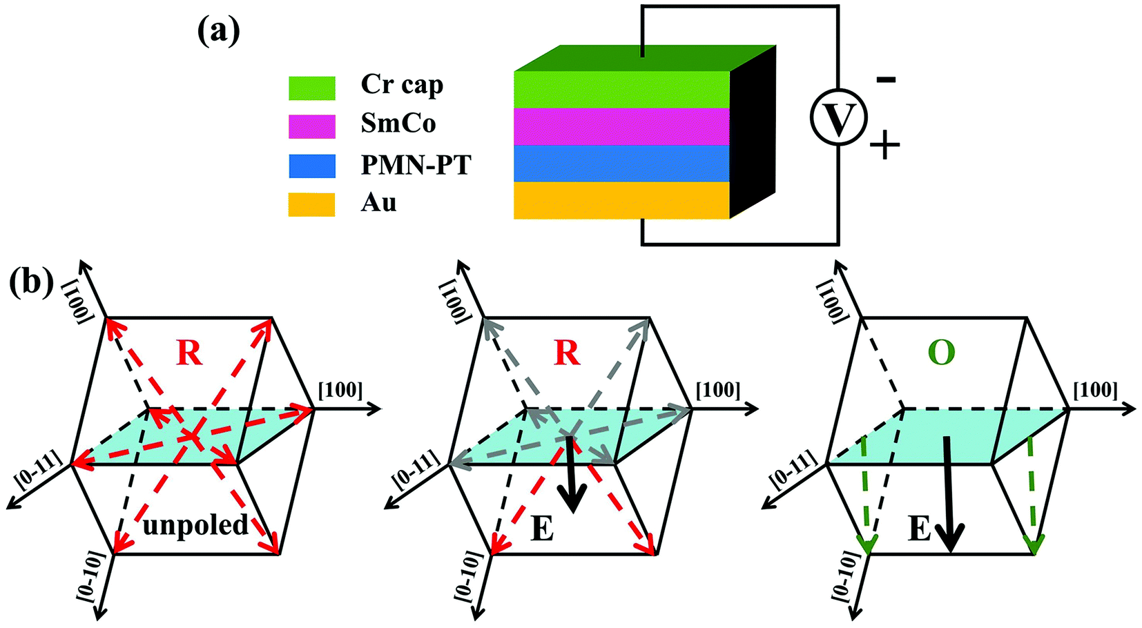 | ||
| Fig. 1 (a) Configuration of the SmCo/(011)PMN-PT heterostructure. (b) Polarizations of the PMN-PT(011) substrate upon applying an electric field along the [0−1−1] direction, increasing in electric field from left to right. The length of the black arrows represents the magnitude of the electric field. The red and green arrows represent the polarization directions for the rhombohedral (R) and orthorhombic (O) phases, respectively. The gray arrows represent the polarization directions for R phase that have vanished under the electric field. | ||
Fig. 2 shows the hysteresis loops of the Cr (50 nm)/a-SmCo (50 nm) film grown on PMN-PT(011) measured with magnetic field along the in-plane [100] and [01−1] directions (“a” indicates amorphous). The squareness ratio of the hysteresis loop along the [01−1] direction is much better and the corresponding coercive field is relatively lower than that along the [100] direction. This uniaxial in-plane anisotropy provides the possibility for applications in information storage and spintronics.40–44 The anisotropy constant, kA, calculated by 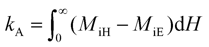 ,56 is about 2.1 × 10⁴ J m−3. The origin of the constant is closely related to the anisotropic strain caused by the difference in lattice constants along the two in-plane directions,34
 . It has been demonstrated that the preferential seeding of FM domains along the elongated direction36,57 and the directional pair ordering53,58 introduced by the anisotropic strain can both lead to uniaxial in-plane magnetic anisotropy in amorphous SmCo films. The coercivities, Hc, along [100] and [01−1] are ∼650 and 500 Oe, respectively, and are among the large ones compared with previously reported magnetically hard amorphous SmCo films.43,44,51–53 The transition parameter between different magnetization directions is expressed as
 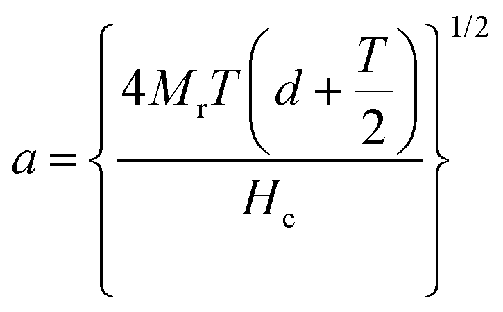 , where Mr is the magnetic remanence, T is the medium thickness, and d is the head-disk spacing.59 Increasing the coercive force decreases the transition parameter, a, which guarantees a high recording density.40
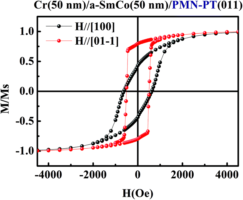 | ||
| Fig. 2 Hysteresis loops of Cr (50 nm)/a-SmCo (50 nm) films grown on PMN-PT(011) substrates, where “a” indicates amorphous. | ||
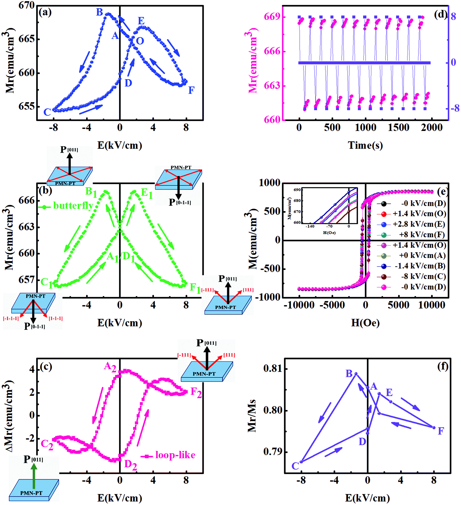
Fig. 3(a) shows the dependence of the remnant magnetization, Mr, on electric field (Mr–E curves) for the in-plane [100] direction. Before applying the electric field, the film was first magnetized by applying a magnetic field of up to 1 T along the in-plane [100] direction, and then reducing the field to zero. The Mr–E curve turn out to be a loop-like behavior, or rather, a mixture composed of the loop-like behavior and butterfly behavior. For the (1 − x)PMN-xPT single crystals near the MPB (x = 0.28–0.32), R–O phase transition can be induced by an electric field, E.55,60,61 The numerical value of critical E decreases monotonically from ∼10 to ∼2 kV cm−1 as the PT concentration increases from x = 0.28 to 0.32, and an irreversible R–O phase transition and strain memory effect occurs at x = 0.32.62 Although the commercial (1 − x)PMN-xPT substrate used in the present work has a nominal composition of x ∼0.30, the possibility of component inhomogeneity may lead to different critical E. In other words, within ±8 kV cm−1, part of R phase may remain stable and non-180° (71° and 109°) polarization switching contributes to the butterfly-like behavior, whereas the other part contributes to the loop-like behavior arising from the irreversible R–O phase transition induced by E.55,62 Separating the Mr–E curves into symmetric butterfly-like and antisymmetric loop-like parts provides a clearer picture (Fig. 3(b) and (c)). Details and sketches indicating electric field-induced polarization switching and the R–O phase transition are provided in ESI S1.† We also measured the strain–electric field curves (Fig. S5a†) and polarization–electric field curve (Fig. S5b†), which are consistent with the asymmetric Mr–E curves (ESI S3†). Moreover, we performed X-ray diffraction (Fig. S3†) and XRD-RSMs (Fig. S4†) under in situ electric fields, and the results confirmed our hypothesis and strongly supported the irreversible R–O transition (ESI S2†).
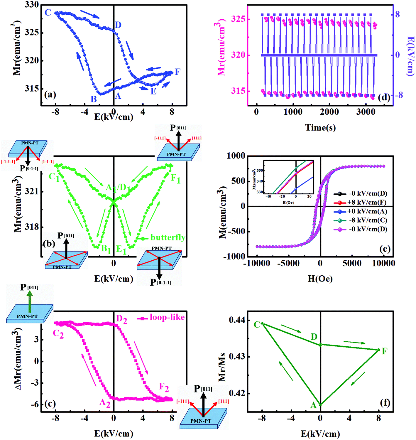 | ||
| Fig. 3 (a) Dependence of the remnant magnetization on the electric field (Mr–E curves) for the in-plane [100] direction, from which the decomposed (b) butterfly-like and (c) loop-like parts are obtained. (d) Repeated Mr pulse measurements. (e) Magnetic hysteresis loops with the magnetic field along the in-plane [100] direction, where the electric field was applied in the sequence of −0(D), +8(F), +0(A), −8(C), −0(D) kV cm−1. For consistency, the capital letters in parentheses correspond to those shown in (a) and the first M–H curve here was measured when PMN-PT was in O phase. Inset: magnification of the M–H curves. (f) Dependence of Mr/Ms on the electric field corresponding to (e). The arrows represent the electric field application sequence. | ||
During the variation of the electric field, the non-180° polarization switching in R phase causes the volatile butterfly-like Mr–E curve (Fig. 3(b)). The application of a −8 kV cm−1 electric field (A1–B1–C1) decreases, and then increases Mr, and the turning point lies in the coercive field, Ecr (point B1). In this process, the preferential polarization directions of the substrate change from [−111] and [111] (point A1) to the four possible in-plane 〈111〉 directions (point B1), and then rotate to [1−1−1] and [−1−1−1] (point C1). The compressive strain along the [100] direction, induced by the polarization reorientation of the substrate, decreases, and then increases, correspondingly. The zero electric field here (point A1) comes from the positive electric field, so there are two preferential polarization directions ([−111], [111]) rather than eight possible 〈111〉 polarization directions. When the electric field is removed from point C1 to D1, Mr decreases linearly. The domain structure of the substrate at point D1 remains basically the same as that at point C1 ([1−1−1], [−1−1−1]). However, the emergence of a small proportion of the non-180° (71° and 109°) polarization switching cannot be excluded during the decreasing procession of the electric field (C1–D1),63 so that the compressive strain at point D1 is not as large as that at point C1. Next, we address the fact that the two points A1 and D1 represent different domain structures (Fig. S2a and S2d†) though their positions in Fig. 3(b) are the same. The preferential polarization directions are [−111] and [111] at point A1, whereas they are [1−1−1] and [−1−1−1] at point D1. When the electric field is applied in reverse (D1–E1–F1–A1), the variation of the compressive strain and the corresponding remnant magnetization remains similar and the polarization direction is the opposite. Then, the butterfly-like behavior comes into being. The compressive strain along the in-plane [100] direction reaches its maximum when the electric field reaches its maximum (points C1 and F1), and the minimum compressive strain occurs at the coercive field, Ecr (points B1 and E1). The contribution of the butterfly-like behavior causes the coercive field in Fig. 3(a). The variation of the remnant magnetization and the compressive strain along the [100] direction are similar. The larger compressive strain results in the higher remnant magnetization.
During changing the electric field, the irreversible R–O phase transition (Fig. 3(c)) coincides with the polarization reorientation in R phase. That is, when the electric field increases to −8 kV cm−1 (point C2), the irreversible R–O phase transition occurs and some parts of the polarizations rotate to the [011] direction (Fig. 3(c)). The strain induced by the R–O phase transformation along the in-plane [100] direction is also compressive and the amplitude is even larger than the strain induced by the polarization switching in the R phase (Fig. 1(b)). When the electric field decreases to −0 kV cm−1 from point C2 to D2, the structure of O phase and the polarization direction remain due to the irreversibility of the R–O phase transition, as does the compressive strain. When the electric field increases to +8 kV cm−1, from point D2 to F2, the substrate returns to R phase and remains unchanged, even when the electric field decreases to +0 kV cm−1, from point F2 to A2. Although the strain in this procession (O–R phase transformation) is still compressive, it is a strain release procession, rather than a strain accumulation procession. The loop-like part of the Mr–E behavior, or the irreversibility of the R–O phase transformation, leads to the non-volatility of the modulation. What needs to be explained is that the irreversibility means that the R–O phase transformation is not reversible in the only-positive/only-negative electric field. As shown in Fig. 3(c), the relative remnant magnetization in O phase is higher than that in R phase because the compressive strain in O phase is larger than that in R phase along the [100] direction. This phenomenon reflects the same rule—the bigger the compressive strain, the higher the Mr—compared with the butterfly-like part shown in Fig. 3(b). Owing to the loop-like behavior in the Mr–E curves contributed to by the R–O phase transformation, there are two Mr states with different magnetization values at E = ±0 kV cm−1. In this case, the magnetization does not return to the initial state as soon as the driving electric field is removed, but goes to another Mr state. That is, a nonvolatile electric-field-controlled magnetization at room temperature has been achieved in an amorphous SmCo/PMN-PT(011) heterostructure, and it is the first time to catch sight of the marvellous spectacle in amorphous SmCo alloys.
The remnant magnetization (Mr) of the amorphous SmCo film can be regulated by bipolar electric fields and it is nonvolatile (Fig. 3(a)); therefore, stable and remarkable high and low Mr states can be obtained by switching the polarity of the electric field (Fig. 3(d)). The switching of the two Mr states was measured with intermittent positive and negative pulsed electric fields of ±8 kV cm−1. The reversible Mr induced by the pulsed electric fields is promising for applications in two-state memory devices.64Fig. 3(e) shows the magnetic hysteresis loops (M–H curves) of the amorphous SmCo thin film on PMN-PT(011) measured under a magnetic field along the in-plane [100] direction, where the electric field was applied in the sequence −0 (D), +8 (F), +0 (A), −8 (C), −0 (D) kV cm−1. ±0 kV cm−1 indicates zero positive or negative electric field. For consistency, the capital letters in parentheses in Fig. 3(e) correspond to those in Fig. 3(a), and the first M–H curve was measured when PMN-PT was in O phase. Due to the repeatability of the cycles, we choose the M–H curve under an electric field of −0 kV cm−1 (D), rather than +0 kV cm−1 (A), to start the M–H measurements. Overall, there are no major differences among the curves. Nevertheless, Mr clearly changes with the applied electric field if the intersection of the curves and the vertical axis are magnified (inset of Fig. 3(e)). Furthermore, the dependence of Mr/Ms, where Ms is the saturated magnetization, on the electric field (Mr/Ms–E curve) for the in-plane [100] direction is shown in Fig. 3(f). The maximum change of Mr/Ms from 0.416 to 0.439 occurs when the electric field is changed from +0 (point A) to −8 kV cm−1 (point C), and the relative Mr change [Δ(Mr/Ms)/((Mr/Ms)(0))] is about −5.8%, which is consistent with the data shown in Fig. 3(a) and is comparable to a previous result reported for CoFe2O4/PMN-PT.30 The same behavior can be observed in Fig. 3(d)–(f). The maximum remnant magnetization occurs at −8 kV cm−1, namely, the electric field at which the maximum compressive strain along the [100] direction is reached.
These results show that a large compressive strain is produced along the in-plane [100] direction when the electric field is applied along the out-of-plane [011] direction and the remnant magnetization increases with the compressive strain. In other words, the magnetization process along the initially hard direction of the amorphous SmCo film becomes easier when the electric field is applied across the thickness direction of the substrates, which is the opposite of that described in (011)-Pr0.7Sr0.3MnO3/PMN-PT.36 Our previous results36 revealed that the magnetization process became easier along the easy axis and harder along the hard axis under applied electric fields in (011)-Pr0.7Sr0.3MnO3/PMN-PT. The difference in behavior in this work, namely, the increase of Mr along the hard axis, arises from the electric-field-induced effective uniaxial magnetic anisotropy field, Heff,〈100〉, in amorphous SmCo films. In a multiferroic heterostructure, an applied electric field induces a strain on the piezoelectric layer, and this strain is transferred to the magnetic layer. Hence, the magnetoelastic energy (FME) emerges as required and Heff, defined as  , comes into being immediately.65 After a series of derivations, Heff,〈100〉 can be expressed as
  ,65,66 where σ[100]
 and σ[01−1]
 are compressive stress along the [100] direction and tensile stress along the [01−1] direction, respectively. Finally, Heff,〈100〉 is expressed as
  ,65,66 where λ is the magnetostriction coefficient of amorphous SmCo films (Sm4Co96, λ = −16 × 10−6; Sm10Co90, λ = −37 × 10−6; Sm27Co73, λ = −51 × 10−6).46 The nominal composition of our film is SmCo5, between Sm10Co90 and Sm27Co73, so −40 × 10−6 was chosen as the value of λ. Y is the Young's modulus of amorphous SmCo film (120 GPa),46ν is the Poisson's ratio (0.27),46Ms is the saturation magnetization of amorphous SmCo film (850 emu cm−3), and d31 and d32 are the in-plane piezoelectric coefficients along the [100] and [01−1] directions (−3100 and 1400 pC N−1), respectively, for the (011)-cut PMN-PT substrate.10,67,68 Thus, a rough value of Heff,〈100〉, as large as 500 Oe, was obtained with an electric field of ±8 kV cm−1, which is comparable to the coercive field of 600 Oe along the hard axis. The electric-field-induced effective uniaxial magnetic anisotropy in the amorphous SmCo film along the [100] hard axis could promote the magnetization process, resulting in an increase of Mr. A brief ideal sketch is shown in Fig. 4 to illustrate this procession. When the substrate is unpoled, the easy axis lies in the [01−1] direction (Fig. 4(a)). When the substrate is poled, the magnetization process along the [100] direction is promoted under the effect of Heff,〈100〉 (Fig. 4(b)). This theoretical conclusion is broadly in line with the experimental results. Similarly, a reduction of Mr along the [01−1] easy axis was observed due to the −500 Oe of Heff,〈01−1〉
 .62 Here, the in-plane stress provided by the substrate was assumed to be transmitted completely to the film grown on it, ignoring factors that may reduce the stress. The relevant parameters, Y, λ, and ν, were taken from the data provided for commercial SmCo magnets.46
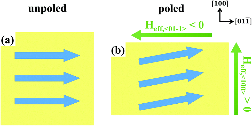 | ||
| Fig. 4 Schematics of the magnetization states in the film in the (a) unpoled and (b) poled states of the substrate. The films experience compression along the [100] direction and extension along the [01−1] direction during polarization. The blue arrows denote the spin directions and their rotation in the poled state, where Heff, produced by the specific magnetostrictive properties of the amorphous SmCo thin film and the anisotropic strain from the PMN-PT substrate, rotates the easy axis. | ||
The trends for |Heff,〈100〉| (or |Heff,〈01−1〉|) and the strain with the variation of the electric field remain the same,69 and are responsible for the modulation of Mr (Fig. 3(f)). When the negative electric field is applied (points A–B–C, Fig. 3(a)), the compressive strain along [100] direction decreases, increases, and then reaches the maximum at point C, as does the effect of Heff,〈100〉, and Mr reaches its maximum at point C. After that, with decreasing electric field along path C–D, the compressive strain and Heff,〈100〉 decrease, and Mr also decreases. When the negative electric fields are applied, especially from −Ecr to −8 kV cm−1, the non-180° (71° and 109°) polarization switching in R phase leads to the accumulation of the compressive strain during the whole butterfly-like procession. In addition, the irreversible R–O phase transformation allows the compressive strain to reach a new maximum. The combination of these two factors is responsible for the maximum of Heff and the remnant magnetization. When the positive electric fields are applied (D–E–F–A, Fig. 3(a)), the trends for Mr and |Heff,〈100〉| (or |Heff,〈01−1〉|) with the variation of electric field are also similar. However, the changes in Mr under the positive electric fields are much smaller than those under the negative fields for the following reason. When a positive electric field is applied (D–E–F, Fig. 3(a)), the butterfly-like part accumulates the compressive strain (D1–E1–F1, Fig. 3(b)) on the whole, whereas the loop-like part releases the compression (D2–F2, Fig. 3(c)). This means that the loop-like part is a drag on the comprehensive compressive strain, which results in the smaller |Heff,〈100〉|, as well as the smaller compressive strain compared with the negative electric fields. In conclusion, the effective uniaxial magnetic anisotropy field, Heff,〈100〉, induced by the applied electric fields is mainly responsible for the easier magnetization along the hard axis ([100] direction). Heff,〈100〉 arises from both the magnetostrictive properties of the amorphous SmCo films and the anisotropic strain from the substrate induced by the applied electric field.
The variation of the directional pair ordering in amorphous SmCo film caused by the anisotropic strain may also explain the anisotropy modulation of the magnetization. According to previous studies,53,58,70,71 directional pair ordering can cause in-plane anisotropy in amorphous films. The Co–Co and Sm–Co pairs in amorphous SmCo films are recommended to be the mechanism of the induced anisotropy,70 and the directional pair ordering can be rearranged by the applied stress.72 In crystalline alloys, the rearrangement takes place through atoms jumping from regular lattice sites to neighbouring vacant sites. In amorphous alloys, the so-called free volumes behave similarly to the vacancies in crystalline materials, which correspond to the free spaces between atoms.73 The mobility of the atoms increases around a free volume, and thus increases the rearrangements of the atoms.73 In our samples, the electric-field induced anisotropic strain drives the rearrangement of the directional pairs. An ideal simple schematic of atom pairs’ arrangement is shown in Fig. 5. When the substrate is unpoled, the easy axis lies in the [01−1] direction and the pair arrangement is shown in Fig. 5(a). When the substrate is poled, the films are compressed along the [100] direction and extended along the [01−1] direction during the polarization. More free volumes along the [01−1] direction may emerge. The mobile Sm atoms move to the new free volumes and the number of Sm–Co pairs increases along the [01−1] direction. The direction of the Sm–Co pair's magnetic moment lies in the connection direction of the Sm and Co atoms, which was assumed to be pointing toward the Co atom. Hence, the remnant magnetization along the [100] direction increases and that along the [01−1] direction decreases under the effect of the anisotropic strain induced by the electric field. The behavior of the Co–Co pairs tends to be similar, which is not shown here. It can be concluded that the anisotropic strain provided by the substrate under the electric fields can also affect the rearrangement of the directional pairs in amorphous SmCo films, and then affect the in-plane anisotropy further.
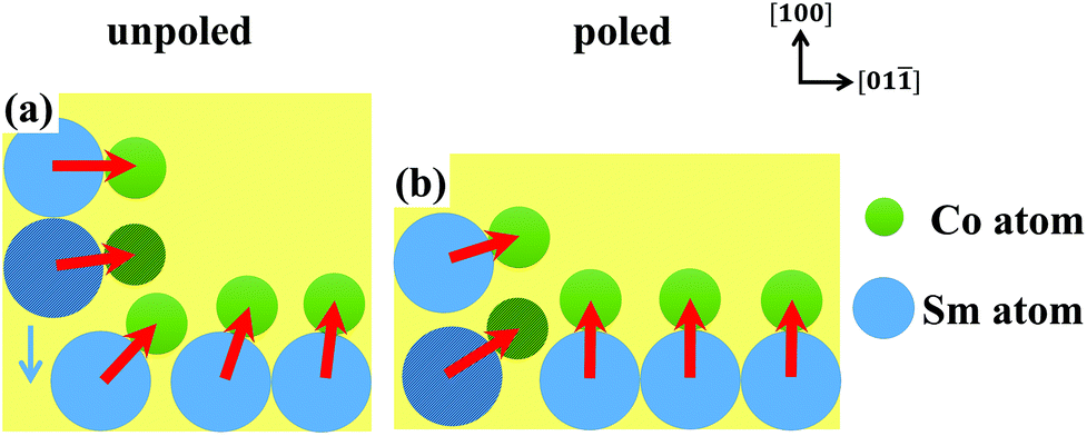 | ||
| Fig. 5 Schematics of pair arrangements in the film in the (a) unpoled and (b) poled states of the substrate. The films experience compression along the [100] direction and extension along the [01−1] direction during polarization. The big blue circles represent Sm atoms, and the small green circles represent Co atoms. The red arrows represent the direction of the Sm–Co pairs’ magnetic moments. | ||
Fig. 6(a) shows the dependence of the remnant magnetization on the electric field (Mr–E curves) for another in-plane [01−1] direction. Before applying the electric field, the film was similarly magnetized by applying a magnetic field of up to 1 T along the in-plane [01−1] direction, and then reducing the magnetic field to zero. There are similarities and differences between the regulation of the magnetic properties by the electric field along the [100] and [01−1] directions. On the one hand, similar to Fig. 3(a), the Mr–E curve along the [01−1] direction is still a mixture of the loop-like and butterfly-like behavior and the two parts are shown separately in Fig. 6(b) and (c), respectively. Two circles appear on the both sides of the loop-like curve, but the reason for this is unclear at the moment. In addition, the remnant magnetization at −8 kV cm−1 arrives at the extremums in both situations (maximum in the [100] direction and minimum in the [01−1] direction) due to the coexistence of R and O phases. On the other hand, for the in-plane [01−1] direction, although the Mr switching by the bipolar electric fields remains, the variation of Mr is the opposite of that along the [100] direction. In particular, the electric-field-induced effective uniaxial magnetic anisotropy in amorphous SmCo film blocks the magnetization process along the [01−1] easy axis, resulting in a decrease in Mr. For example, the remnant magnetization at +8 (point F) and −8 kV cm−1 (point C) reaches minimum values during the variation of the electric field. In addition, the changes in the remnant magnetization, −5.8% and +2.2% (see following paragraph), along the two in-plane directions ([100], [01−1]) are different in both numerical value and sign under the same electric field conditions. This result is explained by the differences in the type and magnitude of strain along the two in-plane directions under the same electric field. The room-temperature strain at 8 kV cm−1 was examined along both the in-plane directions for the (011)-PMN-PT substrate with similar compositions (Fig. S5a†). A large compressive strain (ca. −0.27%) along the [100] direction and a small tensile strain (ca. 0.12%) along the [01−1] direction are observed. We have already explained the appearance of Heff, the relationship between Heff and strain, and the variation of the directional pair ordering, which is responsible for the harder magnetization along the easy axis of the [01−1] direction under applied electric fields.
 | ||
| Fig. 6 (a) Dependence of the remnant magnetization on the electric field (Mr–E curves) for the [01−1] direction, from which the decomposed (b) butterfly-like part and (c) loop-like part were obtained. (d) Repeated Mr pulse measurements. (e) Magnetic hysteresis loops with the magnetic field along the in-plane [100] direction, where the electric field was applied in the sequence of −0(D), +1.4(O), +2.8(E), +8(F), +1.4(O), +0(A), −1.4(B), −8(C), −0(D) kV cm−1. For consistency, the capital letters in parentheses correspond to the ones shown in (a) and the first M–H curve was measured when PMN-PT was in O phase. Inset: Magnification of the M–H curves. (f) Dependence of Mr/Ms on the electric field corresponding to (e). The arrows represent the electric field application sequence. | ||
The high/low remnant magnetization states (Fig. 6d) caused by the pulsed electric field are still stable and remarkable, although the difference between the two Mr states is slightly smaller than that in Fig. 3(d). The magnetic fields and electric fields are the same as those in Fig. 3(d). The magnetic hysteresis loops (M–H curves) with magnetic fields along the in-plane [01−1] direction were measured under different but typical electric fields (Fig. 6(e)). The coercive field, maximum field, and minimum field were chosen as the representative electric fields, and were applied in the sequence of −0(D), +1.4(O), +2.8(E), +8(F), +1.4(O), +0(A), −1.4(B), −8(C), −0(D) kV cm−1 (Fig. 6a). We chose the M–H curve under −0 kV cm−1 (D), rather than +0 kV cm−1 (A), to start the M–H measurements due to the repeatability of the cycles, and the capital letters in parentheses in Fig. 6(e) correspond to the ones in Fig. 6(a) for consistency. Although the M–H curves under different electric fields look similar (Fig. 6e), the partially enlarged detail shown in the inset shows the variation of Mr. Similar to Fig. 3(f), Fig. 6(f) summarizes the effect of the electric field on Mr based on the data from Fig. 6(e). When the electric field changes from +0 to −8 kV cm−1 along points A–B–C, Mr/Ms changes from 0.805 to 0.787 accordingly, and the relative increase of Mr [Δ(Mr/Ms)/((Mr/Ms)(0))] is +2.2%, nearly one-third the magnitude of the −5.8% change for the [100] direction in the numerical data. The difference between the two absolute changes in the remnant magnetization (|Δ(Mr/Ms)[100]| ∼ 0.023, |Δ(Mr/Ms)[01−1]| ∼ 0.018) is far less marked, which confirms the significance of the modulation along the two in-plane directions. The numerical difference of [Δ(Mr/Ms)/((Mr/Ms)(0))] along the two in-plane directions arises from the different magnitude and sign of the strain, and the intrinsic anisotropy of the amorphous SmCo films. In addition, the negative (positive) value of [Δ(Mr/Ms)/((Mr/Ms)(0))] in the [100] ([01−1]) direction is consistent with the reduction (increase) of Mr as the electric field is applied, which indicates that the magnetization process along the hard (easy) axis is facilitated (blocked) by the effect of the electric-field-induced effective uniaxial magnetic anisotropy.
Generally, the nonvolatile modulation of magnetization in FM-material/PMN-PT heterostructures can be achieved by three methods. The 109° polarization switching is used to produce the nonvolatile control along the [110] direction when the substrate is [001]-poled.2 For the [011]-poled PMN-PT, the non-180° (71°/109°) polarization switching from the out-of-plane to in-plane direction induced by unipolar action can also lead to the nonvolatile regulation.28 The irreversible R–O phase transformation could be another possible cause for the composition of PMN-PT(011) around the MPB.55 In our work, the unipolar action is feasible and the irreversible R–O phase transformation occurs; thus, these effects can be combined. We chose the [01−1] direction and tried to create the unipolar Mr–E curves to make the manipulation less volatile. As mentioned before, O phase prevails when the electric field is negative, so that we selected the positive coercive field (Ecr ∼+3 kV cm−1) as the maximum electric field to form the unipolar cycle (−8 kV cm−1–+3 kV cm−1).
Fig. 7(a) shows the unipolar Mr–E curves along the [01−1] direction for electric field cycled between +3 and −8 kV cm−1. When a positive electric field is applied from −0 to Ecr (points D to E in Fig. 7a), the magnetization response follows the bipolar Mr–E curve with a nonlinear magnetization jump, which mainly corresponds to the 71° or 109° polarization reorientation from [−1−1−1] or [1−1−1] to the four in-plane 〈111〉 directions in R phase. Removing the electric field at Ecr (points E to A) results in a large Mr at point A and the polarization variants remain. When a negative electric field is applied from +0 to −8 kV cm−1 (points A to C), the magnetization response jumps back to the original path compared with Fig. 6(a), because of the non-180° polarization reorientation from the four in-plane 〈111〉 directions to [−1−1−1] or [1−1−1], as well as the irreversible R–O phase transformation. When the electric field is removed (points C to D), the Mr returns (point D). Therefore, two reversible Mr states with different magnetization values at E = ±0 kV cm−1 are created.
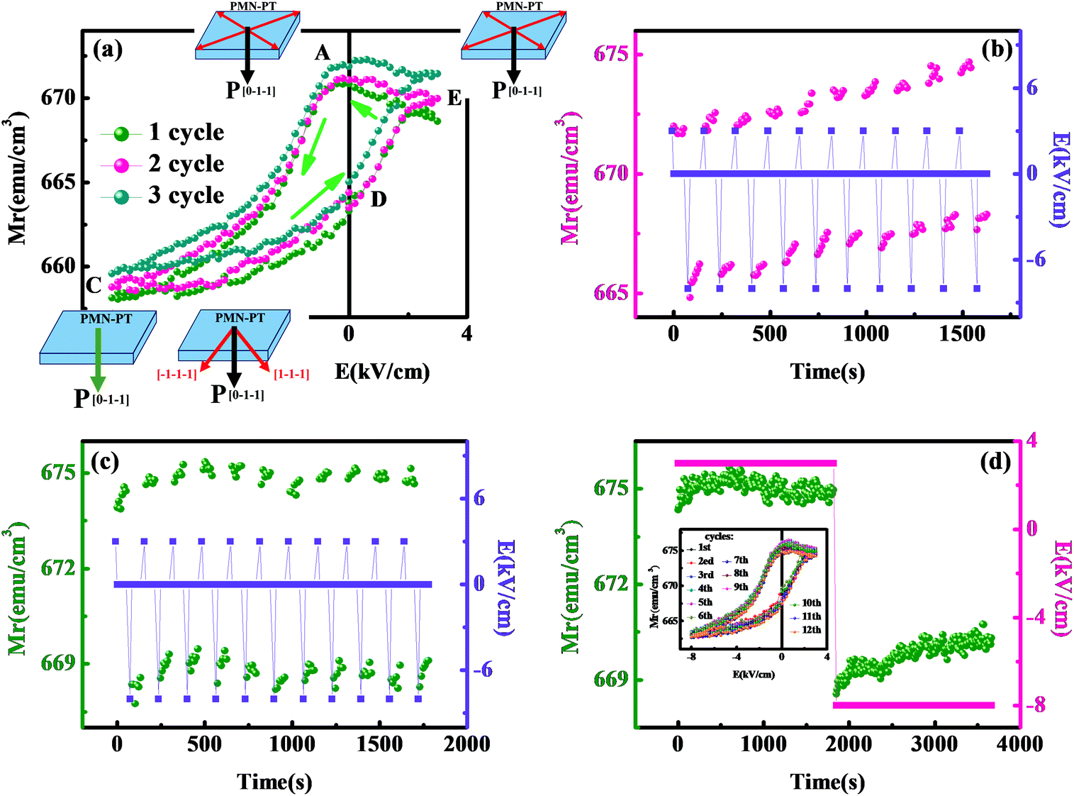 | ||
| Fig. 7 (a) Unipolar Mr–E curves along the [01−1] direction for electric field cycled between +3 and −8 kV cm−1. To avoid confusion, the letters (A/C/D/E) here represent the same electric fields as those in Fig. 5(a). The arrows represent the electric field application sequence. (b) Repeated Mr pulse measurements after the first three unipolar Mr–E curves. (c) Repeated Mr pulse measurements after more than 50 unipolar Mr–E curves and holding for 30 min. (d) Retention of the magnetization states after positive and negative electric field pulses. Inset of (d) shows the last 12 unipolar Mr–E curves. | ||
In Fig. 7(a), the coercive field values remain almost constant, but the magnetization increases slightly shifts in the first three cycles. The repeated Mr pulse measurements (Fig. 7(b)) also indicate that both the high and low magnetization states caused by the pulsed electric field go all the way up. After more than 50 cycles and holding for 30 min, the repeated Mr pulse measurements were carried out again, and surprisingly, the results in Fig. 7(c) show a more stable state. The evolution of Mr from an unstable to a relatively stable state after unipolar cycles should be completely determined by the substrates, which is probably due to the FE history-dependent properties. Namely, the realignment of the four in-plane 〈111〉 polarization variants decides the nonlinear magnetization response. The polarization variants follow the same path when the realignment path is established, while the path may be dictated by the internal friction in the first few cycles.63 In other words, the switching of the polarization from the four in-plane 〈111〉 directions to [−1−1−1] or [1−1−1], as well as the R–O transition, and the reverse path are not streamlined enough at first. The path only became smooth after a number of unipolarization cycles. This helps to explain the shifting of the magnetization in the first three cycles of the unipolar Mr–E curves as well as the “all the way up” in the repeated Mr pulse measurements, shown in Fig. 7(b). Although the magnetization states in Fig. 7(c) are more stable than those in Fig. 7(b), there are still some discrepancies with Fig. 3(d) and 6(d). The reason for the differences is that the realignment of the polarization variants in the first few unipolar cycles is in a metastable state; thus, the states cannot be as stable as the initial condition. In other words, although the realignment path followed by the polarization variants is established, it cannot be as smooth as the original path and a small amount of friction is inevitable.63Fig. 7(d) shows the retention of the magnetization states after positive and negative electric field pulses. The unevenness of the points further illustrates the metastability of the new state. The inset of Fig. 7(d) shows the last 12 unipolar Mr–E curves. These last 12 cycles show high repeatability, which suggests that the magnetization states gradually become stable after frequent cycles. Thus, two stable and reversible magnetic states can also be realized by unipolarizing the substrate. The switching of the polarization in R phase, as well as the R–O phase transformation play major roles in this nonvolatile manipulation.
4. Conclusions
Tunable anisotropic nonvolatile electrical modulation of magnetization at room temperature was achieved in a heterostructure composed of (011)-cut PMN-PT and amorphous SmCo film with uniaxial in-plane anisotropy and hard magnetic properties. When a poled electric field was applied along the out-of-plane [011] direction, the magnetization of the SmCo film became easier along the in-plane [100] hard axis and harder along the in-plane [01−1] easy axis. The effect of anisotropic strain from the PMN-PT substrate and the specific magnetostrictive properties of the amorphous SmCo thin film produced an effective uniaxial magnetic anisotropic field, which caused the novel anisotropic tunability. The variation of the directional pair ordering in the amorphous SmCo film owing to the anisotropic strain also contributed to the electrical modulation of the magnetization. Moreover, the nonvolatile change of Mr and the stable two-state memory effect were demonstrated under a bipolar electric field. Decomposition of the Mr–E curves, in situ XRD studies and in situ XRD-RSMs revealed that the R–O phase transformation played a key role in the nonvolatility. A number of cycles of unipolarization of the FE substrate also established stable nonvolatile magnetization. The present work extends the scope of electric-field-controlled magnetization to hard magnetic films, which is desirable for designing new multifunctional devices, particularly electric-write nonvolatile high-density MRAM based on SmCo amorphous films.Conflicts of interest
There are no conflicts to declare.Acknowledgements
This work was supported by the National Basic Research Program of China (973 program, Grant No. 2017YFB0702702, 2018YFA0305704 and 2016YFB700903), the National Natural Sciences Foundation of China (Grant No. 51531008, 51771223, 51590880, U1832219, 11474341 and 11674378), the Inner Mongolia Science and Technology Major Project of China 2016, and the Strategic Priority Research Program (B) and key program of the CAS.References
- W. Eerenstein, M. Wiora, J. L. Prieto, J. F. Scott and N. D. Mathur, Nat. Mater., 2007, 6, 348–351 CrossRef CAS PubMed.
- S. Zhang, Y. G. Zhao, P. S. Li, J. J. Yang, S. Rizwan, J. X. Zhang, J. Seidel, T. L. Qu, Y. J. Yang, Z. L. Luo, Q. He, T. Zou, Q. P. Chen, J. W. Wang, L. F. Yang, Y. Sun, Y. Z. Wu, X. Xiao, X. F. Jin, J. Huang, C. Gao, X. F. Han and R. Ramesh, Phys. Rev. Lett., 2012, 108, 137203 CrossRef CAS PubMed.
- N. X. Sun and G. Srinivasan, Spin, 2012, 02, 1240004 CrossRef.
- C. A. Vaz, J. Phys.: Condens. Matter, 2012, 24, 333201 CrossRef CAS PubMed.
- N. A. Spaldin, S. W. Cheong and R. Ramesh, Multiferroics: Past, present, and future, Phys. Today, 2010, 63, 38–43 CrossRef.
- C. W. Nan, M. I. Bichurin, S. Dong, D. Viehland and G. Srinivasan, J. Appl. Phys., 2008, 103, 031101 CrossRef.
- T. Nan, Z. Zhou, M. Liu, X. Yang, Y. Gao, B. A. Assaf, H. Lin, S. Velu, X. Wang, H. Luo, J. Chen, S. Akhtar, E. Hu, R. Rajiv, K. Krishnan, S. Sreedhar, D. Heiman, B. M. Howe, G. J. Brown and N. X. Sun, Sci. Rep., 2014, 4, 3688 CrossRef PubMed.
- Y. L. Zhao, Q. P. Chen, Y. G. Zhao, L. Pan and Y. Sun, Appl. Phys. Lett., 2013, 103, 082905 CrossRef.
- S. E. Park and T. R. Shrout, J. Appl. Phys., 1997, 82, 1804–1811 CrossRef CAS.
- S. Zhang, Y. Zhao, X. Xiao, Y. Wu, S. Rizwan, L. Yang, P. Li, J. Wang, M. Zhu, H. Zhang, X. Jin and X. Han, Sci. Rep., 2014, 4, 3727 CrossRef PubMed.
- S. Takei, A. Morisako and M. Matsumoto, J. Appl. Phys., 2000, 87, 6968–6970 CrossRef CAS.
- M. Fiebig, J. Phys. D: Appl. Phys., 2005, 38, R123–R152 CrossRef CAS.
- A. Singh, V. Neu, R. Tamm, K. Rao, S. Faehler, W. Skrotzki, L. Schultz and B. Holzapfel, J. Appl. Phys., 2006, 99, 08E917 CrossRef.
- K. Roy, S. Bandyopadhyay and J. Atulasimha, Appl. Phys. Lett., 2011, 99, 063108 CrossRef.
- W. Eerenstein, N. D. Mathur and J. F. Scott, Nature, 2006, 442, 759–765 CrossRef CAS PubMed.
- N. Jedrecy, H. J. von Bardeleben, V. Badjeck, D. Demaille, D. Stanescu, H. Magnan and A. Barbier, Phys. Rev. B: Condens. Matter Mater. Phys., 2013, 88, 121409(R) CrossRef.
- N. Li, M. Liu, Z. Zhou, N. X. Sun, D. V. B. Murthy, G. Srinivasan, T. M. Klein, V. M. Petrov and A. Gupta, Appl. Phys. Lett., 2011, 99, 192502 CrossRef.
- M. Liu, O. Obi, J. Lou, Y. Chen, Z. Cai, S. Stoute, M. Espanol, M. Lew, X. Situ, K. S. Ziemer, V. G. Harris and N. X. Sun, Adv. Funct. Mater., 2009, 19, 1826–1831 CrossRef.
- N. A. Pertsev, H. Kohlstedt and R. Knöchel, Phys. Rev. B: Condens. Matter Mater. Phys., 2011, 84, 1 CrossRef.
- L. Shu, Z. Li, J. Ma, Y. Gao, L. Gu, Y. Shen, Y. Lin and C. W. Nan, Appl. Phys. Lett., 2012, 100, 022405 CrossRef.
- M. Liu, Z. Zhou, T. Nan, B. M. Howe, G. J. Brown and N. X. Sun, Adv. Mater., 2013, 25, 1435–1439 CrossRef CAS PubMed.
- S. M. Wu, S. A. Cybart, P. Yu, M. D. Rossell, J. X. Zhang, R. Ramesh and R. C. Dynes, Nat. Mater., 2010, 9, 756–761 CrossRef CAS PubMed.
- V. Laukhin, V. Skumryev, X. Marti, D. Hrabovsky, F. Sanchez, M. V. Garcia-Cuenca, C. Ferrater, M. Varela, U. Luders, J. F. Bobo and J. Fontcuberta, Phys. Rev. Lett., 2006, 97, 227201 CrossRef CAS PubMed.
- X. Li, L. Lou, W. Song, G. Huang, F. Hou, Q. Zhang, H. T. Zhang, J. Xiao, B. Wen and X. Zhang, Adv. Mater., 2017, 29, 16 Search PubMed.
- H. J. A. Molegraaf, J. Hoffman, C. A. F. Vaz, S. Gariglio, D. van der Marel, C. H. Ahn and J.-M. Triscone, Adv. Mater., 2009, 21, 3470–3474 CrossRef CAS.
- Y. W. Yin, J. D. Burton, Y. M. Kim, A. Y. Borisevich, S. J. Pennycook, S. M. Yang, T. W. Noh, A. Gruverman, X. G. Li, E. Y. Tsymbal and Q. Li, Nat. Mater., 2013, 12, 397–402 CrossRef CAS PubMed.
- J. Lou, M. Liu, D. Reed, Y. Ren and N. X. Sun, Adv. Mater., 2009, 21, 4711–4715 CrossRef CAS.
- T. Wu, A. Bur, P. Zhao, K. P. Mohanchandra, K. Wong, K. L. Wang, C. S. Lynch and G. P. Carman, Appl. Phys. Lett., 2011, 98, 012504 CrossRef.
- C. Thiele, K. Dörr, O. Bilani, J. Rödel and L. Schultz, Phys. Rev. B: Condens. Matter Mater. Phys., 2007, 75, 054408 CrossRef.
- J. J. Yang, Y. G. Zhao, H. F. Tian, L. B. Luo, H. Y. Zhang, Y. J. He and H. S. Luo, Appl. Phys. Lett., 2009, 94, 212504 CrossRef.
- Y. Chen, T. Fitchorov, C. Vittoria and V. G. Harris, Appl. Phys. Lett., 2010, 97, 052502 CrossRef.
- S. Geprägs, A. Brandlmaier, M. Opel, R. Gross and S. T. B. Goennenwein, Appl. Phys. Lett., 2010, 96, 142509 CrossRef.
- Y. Chen, J. Gao, T. Fitchorov, Z. Cai, K. S. Ziemer, C. Vittoria and V. G. Harris, Appl. Phys. Lett., 2009, 94, 082504 CrossRef.
- M. Liu, B. M. Howe, L. Grazulis, K. Mahalingam, T. Nan, N. X. Sun and G. J. Brown, Adv. Mater., 2013, 25, 4886–4892 CrossRef CAS.
- R. Lo Conte, Z. Xiao, C. Chen, C. V. Stan, J. Gorchon, A. El-Ghazaly, M. E. Nowakowski, H. Sohn, A. Pattabi, A. Scholl, N. Tamura, A. Sepulveda, G. P. Carman, R. N. Candler and J. Bokor, Nano Lett., 2018, 18, 1952–1961 CrossRef CAS.
- Y. Y. Zhao, J. Wang, H. Kuang, F. X. Hu, Y. Liu, R. R. Wu, X. X. Zhang, J. R. Sun and B. G. Shen, Sci. Rep., 2015, 5, 9668 CrossRef CAS PubMed.
- S. Sahoo, S. Polisetty, C. G. Duan, S. S. Jaswal, E. Y. Tsymbal and C. Binek, Phys. Rev. B: Condens. Matter Mater. Phys., 2007, 76, 092108 CrossRef.
- Y. Yang, M. Meng Yang, Z. L. Luo, H. Huang, H. Wang, J. Bao, C. Hu, G. Pan, Y. Yao, Y. Liu, X. G. Li, S. Zhang, Y. G. Zhao and C. Gao, Appl. Phys. Lett., 2012, 100, 043506 CrossRef.
- Y. Liu, F. X. Hu, M. Zhang, J. Wang, F. R. Shen, W. L. Zuo, J. Zhang, J. R. Sun and B. G. Shen, Appl. Phys. Lett., 2017, 110, 022401 CrossRef.
- U. Kullmann, E. Koester and C. Dorsch, IEEE Trans. Magn., 1984, MAG-20, 2 Search PubMed.
- V. S. Speriosu, D. A. Herman, I. L. Sanders and T. Yogi, IBM J. Res. Dev., 1990, 34, 6 Search PubMed.
- M. E. Mchenry and D. E. Laughlin, Acta Mater., 2000, 20, 223–238 CrossRef.
- M. Gronau and H. Goeke, IEEE Trans. Magn., 1983, MAG-19, 5 Search PubMed.
- F. Magnus, R. Moubah, A. H. Roos, A. Kruk, V. Kapaklis, T. Hase, B. Hjörvarsson and G. Andersson, Appl. Phys. Lett., 2013, 102, 162402 CrossRef.
- F. Magnus, R. Moubah, U. B. Arnalds, V. Kapaklis, A. Brunner, R. Schäfer, G. Andersson and B. Hjörvarsson, Phys. Rev. B: Condens. Matter Mater. Phys., 2014, 89, 224420 CrossRef.
- F. Magnus, R. Moubah, V. Kapaklis, A. Brunner, R. Schäfer, G. Andersson and B. Hjörvarsson, Phys. Rev. B: Condens. Matter Mater. Phys., 2014, 89, 134414 CrossRef.
- F. Magnus, M. E. Brooks-Bartlett, R. Moubah, R. A. Pcocter, G. Andersson, T. P. Gase, S. T. Banks and B. Hjörvarsson, Nat. Commun., 2016, 7, 11931 CrossRef PubMed.
- R. Moubah, F. Magnus, V. Kapaklis, B. Hjörvarsson and G. Andersson, Appl. Phys. Express, 2013, 6, 053004 CrossRef.
- R. Moubah, F. Magnus, E. Ostman, Y. Muhammad, U. B. Arnalds, M. Ahlberg, B. Hjorvarsson and G. Andersson, J. Phys.: Condens. Matter, 2013, 25, 416004 CrossRef PubMed.
- J. M. Hu, Z. Li, L. Q. Chen and C. W. Nan, Nat. Commun., 2011, 2, 553 CrossRef PubMed.
- M. Gronau and S. Sprenger, IEEE Trans. Magn., 1984, MAG-20, 1 Search PubMed.
- T. D. Cheung, L. Wickramasekara and F. J. Cadieue, J. Appl. Phys., 1985, 57, 3598–3600 CrossRef CAS.
- K. Chen, H. Hegde, S. U. Jen and F. J. Cadieu, J. Appl. Phys., 1993, 73, 5923–5925 CrossRef CAS.
- Y. Y. Zhao, J. Wang, H. Kuang, F. X. Hu, H. R. Zhang, Y. Liu, Y. Zhang, S. H. Wang, R. R. Wu, M. Zhang, L. F. Bao, J. R. Sun and B. G. Shen, Sci. Rep., 2014, 4, 7075 CrossRef PubMed.
- K. Chen, H. Hegde and F. J. Cadieu, Appl. Phys. Lett., 1992, 61, 1861–1863 CrossRef CAS.
- M. Shanthi and L. C. Lim, J. Appl. Phys., 2009, 106, 11 CrossRef.
- T. Z. Ward, J. D. Budai, Z. Gai, J. Z. Tischler, L. Yin and J. Shen, Nat. Phys., 2009, 5, 885–888 Search PubMed.
- G. Suran, K. Ounadjela and F. Machizaud, Phys. Rev. Lett., 1986, 57, 3109–3112 CrossRef CAS PubMed.
- K. E. Johnson, J. Appl. Phys., 2000, 87, 5365–5370 CrossRef CAS.
- H. Cao, J. Li, D. Viehland and G. Xu, Phys. Rev. B: Condens. Matter Mater. Phys., 2006, 73, 184110 CrossRef.
- D. Viehland and J. F. Li, J. Appl. Phys., 2002, 92, 7690–7692 CrossRef CAS.
- M. Shanthi and L. C. Lim, Appl. Phys. Lett., 2009, 95, 10 CrossRef.
- T. Wu, P. Zhao, M. Bao, A. Bur, J. L. Hockel, K. Wong, K. P. Mohanchandra, C. S. Lynch and G. P. Carman, J. Appl. Phys., 2011, 109, 124101 CrossRef.
- C. Zhang, F. Wang, C. Dong, C. Gao, C. Jia, C. Jiang and D. Xue, Nanoscale, 2015, 7, 4187–4192 RSC.
- M. Liu, O. Obi, Z. Cai, J. Lou, G. Yang, K. S. Ziemer and N. X. Sun, J. Appl. Phys., 2010, 107, 7 Search PubMed.
- X. Xue, Z. Zhou, B. Peng, M. Zhu, Y. Zhang, W. Ren, T. Ren, X. Yang, T. Nan, N. X. Sun and M. Liu, Sci. Rep., 2015, 5, 16480 CrossRef CAS.
- J. Peng, H. S. Luo, D. Lin, H. Q. Xu, T. H. He and W. Q. Jin, Appl. Phys. Lett., 2004, 85, 6221–6223 CrossRef CAS.
- L. Luo, H. Wang, Y. Tang, X. Zhao, Z. Feng, D. Lin and H. Luo, J. Appl. Phys., 2006, 99, 2 Search PubMed.
- B. Peng, C. Zhang, Y. Yan and M. Liu, Phys. Rev. A, 2017, 7, 044015 Search PubMed.
- H. N. Bertram and J.-G. Zhu, Phys. Status Solidi, 1992, 46, 271–371 CAS.
- B. W. Corb, R. C. O'Handley, J. Megusar and N. J. Grant, Phys. Rev. Lett., 1983, 51, 1386–1389 CrossRef CAS.
- B. Hofmann and H. Kronmuller, J. Magn. Magn. Mater., 1996, 152, 91–98 CrossRef CAS.
- H. Kronmuller, Phys. Status Solidi, 1983, 118, 661 CrossRef.
Footnote |
| † Electronic supplementary information (ESI) available. See DOI: 10.1039/c8nr06449k |
| This journal is © The Royal Society of Chemistry 2019 |