
Growth of extended DNTT fibers on metal substrates by suppression of step-induced nucleation†
Maximilian
Dreher
,
Dayeon
Kang
,
Tobias
Breuer
 and
Gregor
Witte
*
and
Gregor
Witte
*
Molekulare Festkörperphysik, Philipps-University Marburg, D-35032 Marburg, Germany. E-mail: gregor.witte@physik.uni-marburg.de
First published on 24th July 2019
Abstract
Due to their anisotropic optoelectronic properties, crystalline organic fibers constitute an interesting class of nanoscale materials with great potential for integration into future optoelectronic devices based on organic–inorganic hybrid systems. While chemical synthesis allows for flexible tailoring of electronic molecular properties, structural control of hybrid structures is hampered by the incompatibility of traditional structuring methods such as, e.g. lithography, with these molecular materials. Therefore, other approaches must be used. Here we examine the formation of crystalline fibers of dinaphthothienothiophene (DNTT), a recently synthesized chemically robust organic semiconductor with high charge carrier mobility, upon film growth on noble metal substrates. Based on a comparison of the film growth on a regularly stepped, vicinal surface, we show that substrate steps affect the azimuthal molecular orientation in the seed layer. In particular, they induce a fiber orientation which competes with that of fibers formed on flat terraces and thereby strongly limits the fiber dimensions. We demonstrate a strategy to suppress this parasitical step-induced fiber nucleation by first exposing Ag(111) surfaces to oxygen, or even briefly to ambient conditions, which causes a selective saturation of the active step sites, while subsequent deposition of DNTT yields strongly enlarged fibers that are epitaxially aligned on the (111) surface.
New conceptsSelf-organization is an important route for structuring molecular materials especially for organic/inorganic hybrid architectures. While molecular materials often form crystalline fibers, their length and orientation is limited by surface defects such as steps of the supports that cannot be prevented even on very perfect, single crystalline substrates, thus drastically restricting their use in device applications. Based on the identification of the initial fiber growth, we introduce here a new concept to suppress the defect-driven fiber nucleation at such substrate defects by selective blocking of active step sites using small molecules, so that the fiber formation is only governed by the intrinsic epitaxial growth on ideal, defect-free surface regions. This not only leads to an exclusive growth of epitaxial fibers but also strongly increases the fiber size to several hundreds of microns. This novel approach is quite versatile and allows a distinct improvement of template assisted growth and thereby the quality of organic/inorganic hybrids. |
Introduction
The use of molecular materials as organic semiconductors (OSC) or dyes for the fabrication of thin-film optoelectronic devices and organic–inorganic hybrid systems has attracted much attention because their electronic properties can be precisely tailored by chemical synthesis.1–3 In contrast to inorganic materials whose strong (covalent) interactions allow the fabrication of thermally stable heterostructures with sharp interfaces as well as lateral micro-structuring by means of lithography processes, molecular materials exhibit much weaker mutual interactions (essentially van der Waals type) and are chemically and thermally less robust. Therefore, an application of these well-established structuring methods to molecular materials is hampered. Instead, the use of spontaneous structure formation and self-organization upon film growth constitutes an important alternative strategy for structuring, especially at organic–inorganic hybrid interfaces. Although the preparation of well-defined and contamination-free films of oligomeric molecular materials is allowed by physical vapor deposition, which enables precise control of their nominal thickness, they often exhibit considerable inhomogeneity of the actual thickness. Instead of layer-by-layer growth, typically pronounced dewetting occurs, leading to the formation of discontinuous islands or fibers.4–6 By contrast, the growth of smooth and crystalline molecular films especially on (single) crystalline metal substrates appears to be rather an exception.7The formation of crystalline molecular fibers was first observed upon growth of para-phenylene films on alkali halides and has attracted particular attention because these aggregates exhibit distinct luminescence properties8,9 and serve as a model system for microwave-guide applications below the diffraction limit.10 Since then, the formation of crystalline fibers has been extensively studied and is observed for several rod-like molecules upon deposition onto various substrates including silicates, metal oxides, alkali halides and boron nitride.6,11–21 Moreover, by using anisotropic substrates as template or specific electrostatic molecule–substrate couplings, an azimuthal alignment of such fibers has been demonstrated.11,14,15,17,18 Interestingly, while anisotropic metal substrates such as fcc(110) or vicinal surfaces can be used to prepare molecular seed layers with well-defined uniaxial molecular alignment,17,21–24 almost no fiber alignment is found in thicker multilayer films.23,24 Only during initial multilayer growth (essentially bilayers) a preferential in-plane alignment is maintained, while in case of the periodically oxidized Cu(110)–O(2 × 1) surface it is also preserved in thicker films.17 Crystalline fibers are frequently observed upon growth of rod-like molecules such as para-quaterphenyl or pentacene on (111)-oriented noble metal surfaces, but these are rather short and exhibit only limited azimuthal alignment.25,26 Complementary studies on polycrystalline gold surfaces demonstrate further that surface defects such as steps critically affect the nucleation, which hampers the development of fibers of mesoscopic length.27 A transfer of this concept, which also allows a controlled preparation of crystalline fibers of high performing OSCs, has not yet been systematically studied. In this regard, dinaphthothienothiophene (DNTT) is an interesting that combines excellent charge carrier mobility with high chemical robustness,28 which allows the preparation of long-term stable OFETs. In previous work it was shown that DNTT forms a commensurate seed layer on the densely packed Au(111) and Ag(111) surfaces, while subsequent multilayer growth proceeds in a Stranski–Krastanov mode yielding rather short crystalline fibers, that appear azimuthally randomly oriented,29 and therefore not suitable for integration in optoelectronic devices.
In the present work we have combined scanning tunneling microscopy (STM), atomic force microscopy (AFM), X-ray diffraction (XRD) and optical microscopy to analyze the DNTT fiber formation on different length scales, ranging from the initial seed layer structure to the crystalline texture and orientation of mesoscopic fibers. This enabled us in particular to identify nano-scale factors that control the orientation and limit the length of such fibers. Based on these results, we develop and validate various strategies to enhance the mesoscopic sized fibers and their orientation on noble metal surfaces. By using a stepped Au(998) surface we have at first analyzed the influence of steps on the structure of the seed layer and the subsequent fiber growth. This shows that steps induce different molecular alignments compared to the undisturbed (111) surface which results in a competing, different fiber orientation. Similar fiber orientations were also found on the (111) surfaces of Ag and Au and are attributed to defect step induced nucleation which limits the fiber size and orientation on the flat surfaces. In a second step we demonstrate that this undesired step-induced nucleation can be deactivated by exposing the Ag(111) surface to oxygen or air. This causes a selective covering of steps by oxygen and thereby deactivates the step-induced fiber nucleation and yields largely enhanced DNTT fibers that are exclusively epitaxially oriented along the 〈1![[1 with combining macron]](https://www.rsc.org/images/entities/char_0031_0304.gif) 0〉Ag azimuth directions.
0〉Ag azimuth directions.
Results and discussions
DNTT seed layer and fiber formation on Au(111) and Ag(111)
We begin with a brief summary of the initial stage of DNTT film growth on Ag(111), which has been studied in detail in a previous work.29 For low coverage the DNTT molecules adopt a planar adsorption geometry and form an oblique unit cell, while for slightly larger coverages a saturated monolayer is formed where every second molecule is inclined (indicated by the reddish molecules in Fig. 1e) yielding a herringbone packing motif similar to the bulk structure. Exemplary STM images of these two monolayer phases together with derived structure models are summarized in Fig. 1 while the unit cell parameters are provided in the ESI,† (Fig. S1). Very similar structures are also reported for DNTT monolayers on Au(111)33 which can be rationalized by the almost identical lattice constants of both noble metals. Due to the sixfold symmetry of the (111) substrate surface both monolayer phases appear in six different domains, which is schematically depicted in Fig. 1c and f. Such a herringbone packing motif in a saturated seed layer on a metal surface is quite interesting as is suggests to overcome the structural misfit between a planar adsorption geometry (commonly found on metals) and the packing motif in the bulk phase. However, upon further DNTT deposition non-contiguous, tall fibers with a height of more than 50 nm and a length of up to 10 μm are formed, hence reflecting a Stranski–Krastanov growth mode as shown in Fig. 1g. Corresponding X-ray diffraction measurements (Fig. S2, ESI†) reveal that these fibers are crystalline and are oriented with their (120) or (12) planes parallel to the Ag(111) surface. While some fibers show short straight segments, appearing preferentially aligned along the 〈10〉Ag azimuth directions, they cluster and form bunches with noticeable azimuthal spread as depicted in Fig. 1g. In our previous work this fiber formation could be rationalized by the lateral structural misfit between the saturated monolayer and the bulk crystal structure of DNTT which prevents the formation of well-ordered crystalline islands of large size,29 but we were unable to further improve the fiber size and alignment.
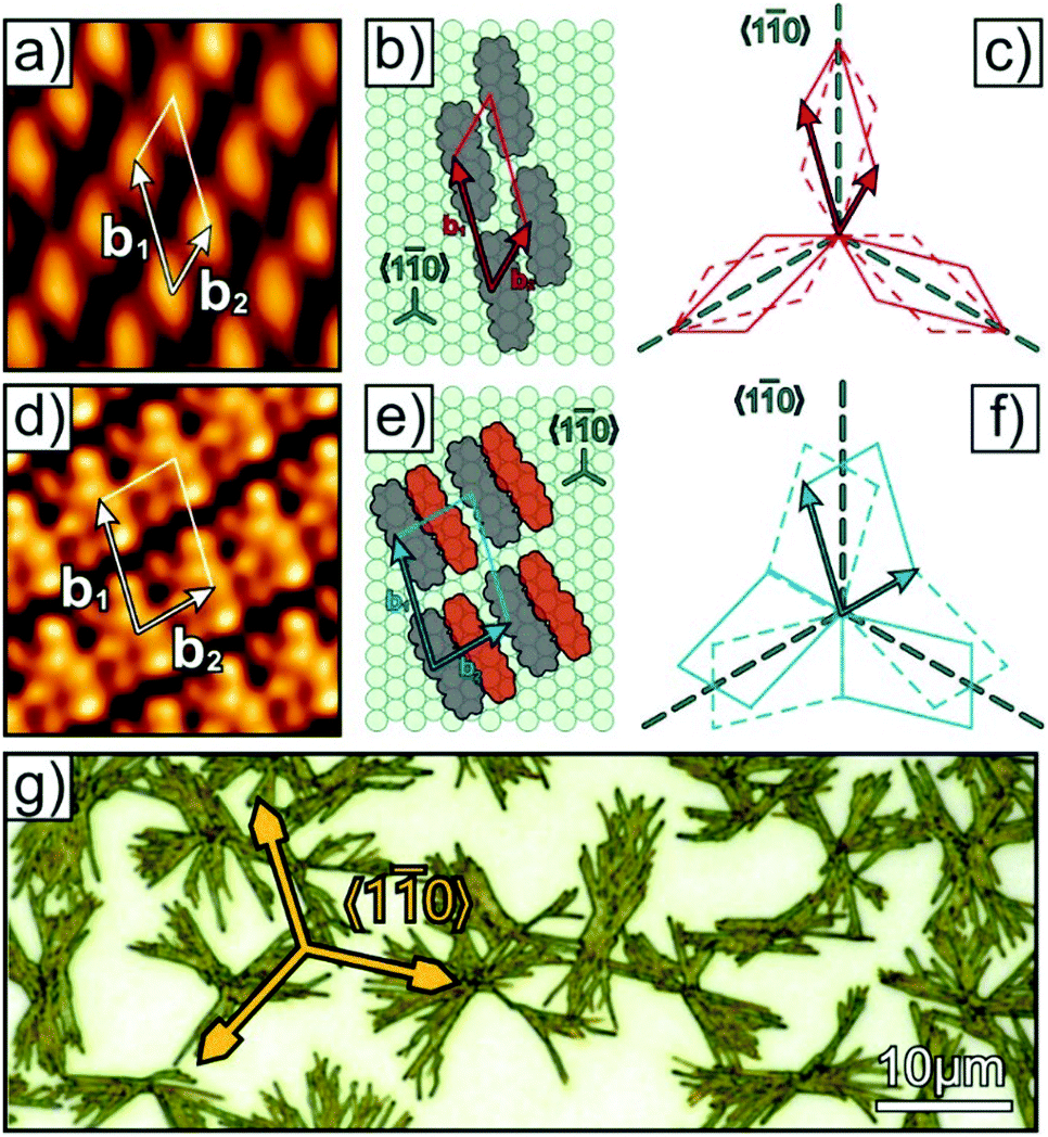 | ||
| Fig. 1 (a) and (d) STM micrographs of planar- and herringbone-monolayer phases of DNTT/Ag(111) (Ubias = −1.92 V, It = 60 pA) together with (b) and (e) structure models. The reddish molecules are not planar oriented but significantly inclined. All adlayer structures appear as rotational and mirror domains on the fcc(111) surface as sketched in (c) and (f). Panel (g) depicts an optical micrograph of a 50 nm thick DNTT film grown on Ag(111) at 340 K. | ||
DNTT film growth on Au(998)
The use of regularly stepped (i.e. vicinal) surfaces is a common strategy to suppress rotational domains and induce uniaxial order in molecular adlayers34,35 because the molecules experience a larger adsorption energy at steps.36 Since very short terraces can prevent a dense packing of adsorbed molecules as compared to a step-free surface and thus affect the lateral packing density,24 larger terraces are desirable because they allow a packing density similar to that on an undisturbed flat surface. On the other hand, with increasing terrace width, vicinal surfaces tend to roughen since entropic contributions favor the formation of kinks, hence limiting the usable terrace width.37 Here we examined an Au(998) surface, which consists of 4.3 nm wide, (111)-oriented terraces that are separated by monatomic steps running along the 〈10〉 azimuth directions (cf.Fig. 2a). At first we analyzed the initial growth of DNTT on Au(998) and compared this arrangement with the reported structures on the (111) surfaces of the noble metals. Fig. 2b shows a typical STM micrograph for a DNTT film with a nominal thickness of 2 Å, which is the expected coverage for one monolayer with flat-lying molecules. In this image one can clearly recognize two gold terraces, where 6 to 7 DNTT molecules are uniformly aligned on each terrace with their long axis parallel to the step edges. Neighboring molecules are slightly shifted and form an oblique unit cell with the vectors b1 = 17 Å and b2 = 8 Å enclosing an angle of 60° on the terraces. This structure is well described by a higher-order-commensurate  phase. This adlayer structure has a molecular surface area of about 110 Å2 which corresponds to a similar packing density as found for the planar DNTT monolayer adopted on the (111) surfaces of silver and gold (∼130 Å2 per molecule), but exhibits a different azimuthal molecular orientation (cf.Fig. 1b). Remarkably, the Au(998) surface appears structurally very stable and shows no reconstruction or faceting upon molecular adsorption, while this is frequently found for other vicinal metal surfaces.38 For slightly larger DNTT coverages a phase transition occurs that parallels the situation found before on the (111) surfaces (cf.Fig. 1d). Fig. 2d shows the beginning of this transformation for a nominal thickness of 2.2 Å on one of the terraces (indicated by the dashed line in Fig. 2d). Although the further developed structure is difficult to image (due to diffusion of admolecules) it allows proposing a structural model. Here, the unit cell is enlarged and exhibits a larger corrugation. This can be understood by adding another molecule and simultaneously levering every second molecule yielding herringbone packing which can be described by a higher-order-commensurate
  phase. Interestingly, in this phase the molecules are stacked slightly differently than in the initial phase and their short sides form an angle of about 67° with respect to the step edge direction (indicated by the blue lines in Fig. 2c and d).
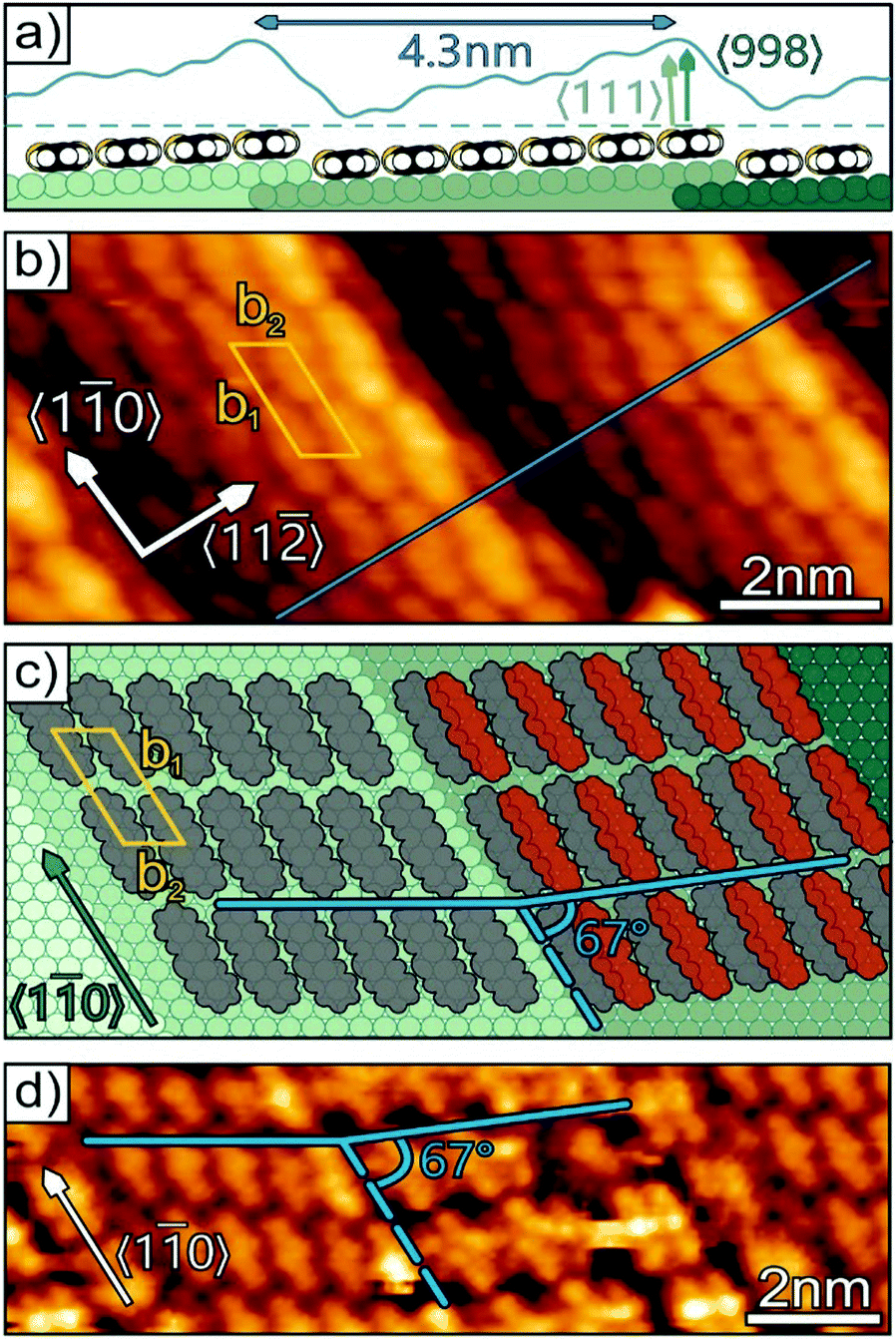 | ||
| Fig. 2 (a) Schematic side view of the Au(998) surface covered with DNTT molecules together with a corresponding line scan (in blue) derived from the STM micrograph (b) of the DNTT seed layer (nominally 2 Å thick), where molecules are aligned with their long axis parallel to the step edges. Panel (c) reveals the molecular packing motif of this seed layer (left side) and the structural change with increasing coverage (right side), which is obtained in the STM micrograph (d), where a slightly larger coverage (2.2 Å) leads to the formation of a herringbone like structure (Ubias = 2.50 V, It = 360 pA). | ||
While the uniform step direction of the vicinal surface effectively suppresses rotational domains in the DNTT adlayer, mirror-domains still can be seen in the STM data as depicted in Fig. 3a and b. Interestingly, not only the unit cell itself, but also the DNTT molecules appear mirrored due to their pro-chiral structure causing chiral domains upon adsorption on surfaces as schematically shown in Fig. 3c. After characterizing the initial growth of DNTT on Au(998), we analyzed if and how the nanoscopic structure of the seed layer is transferred to thicker films. Interestingly, when increasing the DNTT coverage after completion of the seed layer a spontaneous formation of tall fibers with a height of several 10 nm (corresponding AFM data are presented below) takes place, which hampers their microscopic analysis by means of STM. To examine the morphology of mesoscopic films and the azimuthal fiber orientation, we have used optical microscopy as exemplarily shown in Fig. 3d for a 50 nm thick DNTT film deposited onto the Au(998) surface. It reveals the formation of isolated, elongated straight fibers with a length of 10–20 μm and a width of 0.5–1.0 μm that are oriented at an angle of 65° with respect to the gold step edge direction and occasionally appear at the corresponding mirror direction. Corresponding XRD measurements (see Fig. S3, ESI†) show that these fibers are crystalline and again exhibit (120) or (12) contact planes like on the (111) metal substrates. Note that the fibers are much longer than the terrace width of the vicinal surface (10 μm vs. 0.004 μm) demonstrating that the fibers are overgrowing several thousand terraces. The accordance of the molecular stacking direction in the densely packed monolayer and the fiber direction thus demonstrates that the seed layer effectively controls the macroscopic fiber orientation. Although we have clearly demonstrated that the vicinal surface allows a lateral alignment of the DNTT fibers, this approach cannot be scaled up because of limitations in preparing these supports on large dimensions.
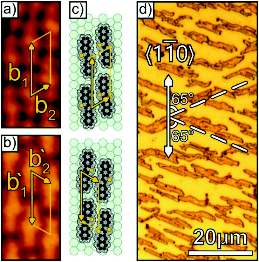 | ||
| Fig. 3 (a) and (b) STM data show two mirror domains of the DNTT seed layer on Au(998) (Ubias = 2.50 V, It = 360 pA), which are schematically depicted in (c). The optical micrograph of a multilayer film on Au(998) with a nominal thickness of 50 nm (d) shows the presence of bidirectional fibers, oriented with an angle of about 65° with respect to the 〈10〉Au direction. | ||
Defect step induced fiber formation and its suppression
With the gained knowledge on the step induced fiber alignment we have revisited the DNTT film growth on Ag(111). As shown in Fig. 1g, DNTT multilayer films exhibit short fibers that are not strictly aligned along high symmetry azimuth directions, but instead form bunches with noticeable azimuthal spread. Comparing this morphology with the distinct fiber alignment dictated by steps as observed for the Au(998) surface, suggests that also defect steps on the (111) surfaces force some fibers to grow along different directions than they would on ideal (111) surfaces without any steps. To test this hypothesis, we further analyzed the initial nucleation and fiber formation with respect to the local surface morphology. Fig. 4a shows an AFM micrograph of the initial stage of DNTT multilayer growth on Ag(111). Despite a nominal film thickness of only 1.5 nm (determined by QCM), isolated and tall fibers with a height of up to 50 nm are formed (cf. Fig. S4, ESI†). These elongated fibers are very narrow (∼200 nm) and run primarily along 〈10〉Ag azimuth directions, that can be recognized in the AFM image as characteristic densely packed step edges (indicated by dashed line in Fig. 4a). A closer inspection reveals additionally branched fibers at an angle of 30° to the preferred fiber directions. This behavior is depicted schematically in Fig. 4b, where the two limiting fiber directions, one parallel and the other at an angle to the step direction are shown in blue and red, respectively. With increasing coverage these limits are filled up yielding bunches with a fan-like fiber distribution.
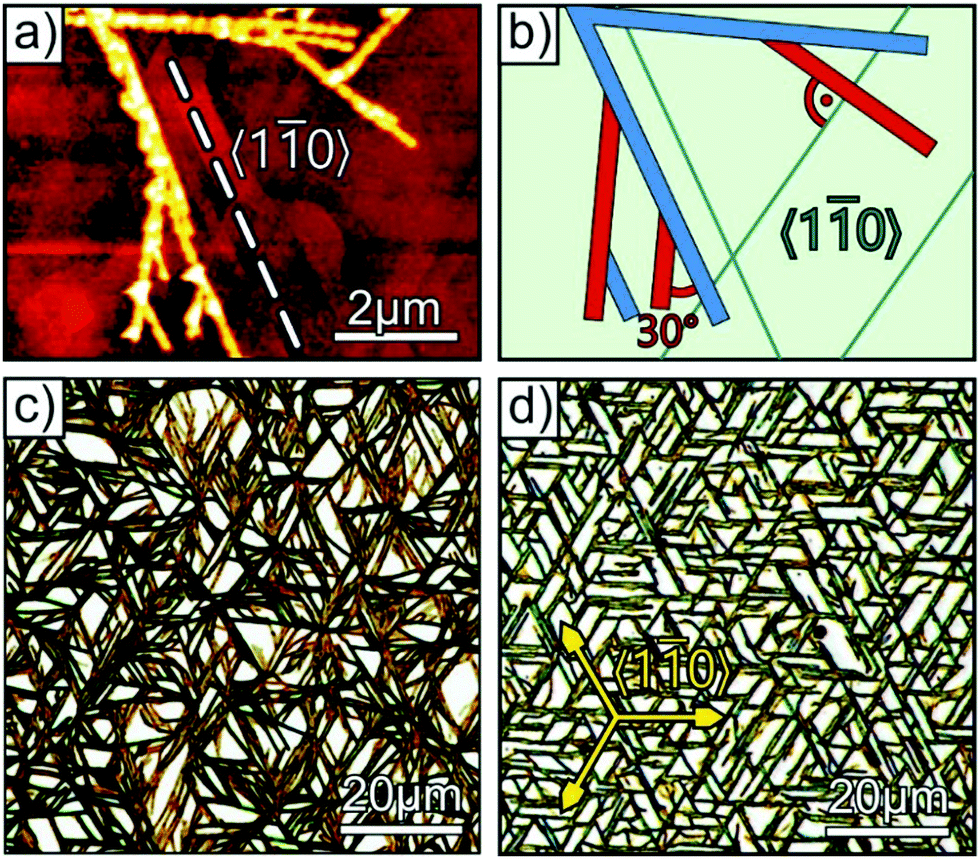 | ||
| Fig. 4 (a) AFM micrograph of a DNTT/Ag(111) film with a nominal thickness of 1.5 nm, together with (b) a scheme showing the azimuthal fiber orientation. AFM micrographs of a 40 nm DNTT grown on oxygen pretreated Ag(111) substrate are shown in (c) for exposure of 500 L and (d) after briefly exposing the surface to ambient conditions. | ||
Next, we have studied a strategy for suppressing this parasitic, step-induced fiber nucleation. To this end, we exploit the fact that adsorption of small molecules leads to a preferred step decoration due to the increased adsorption energy at steps of metal surfaces. Here, we used oxygen, since the rather low sticking coefficient on silver39,40 causes essentially an oxygen adsorption at defects (such as steps) and leaves the defect-free regions largely uncovered. Since molecules experience a reduced substrate interaction on oxides or partially oxidized metal surfaces as compared to clean metals, it is expected that the DNTT fiber formation is decisively determined by the uncovered (111) surface regions. Fig. 4c shows an optical micrograph of a 40 nm DNTT film that was grown at 340 K on a Ag(111) surface which had been exposed to 500 L oxygen before DNTT growth. In contrast to the DNTT film formed on the untreated silver substrate (cf.Fig. 1g), only long fibers running mainly along the 〈10〉Ag directions are formed on the oxygen-treated surface while the parasitic fibers oriented with a rotational offset of 30° are suppressed. Our hypothesis that defect-free surface regions remain essentially free of oxygen is corroborated by the fact that the LEED pattern of the (111) surface is virtually unaffected by this oxygen exposure (cf. Fig. S5, ESI†). A systematic variation of the oxygen uptake shows that the most uniform fibers are obtained for a pre-dosing of 100–2000 L (see Fig. S6, ESI†). Moreover, we note that this pretreatment is rather robust since an improved fiber ordering is even observed for samples that are briefly exposed to ambient conditions. This is impressively demonstrated in Fig. 4d which shows an optical micrograph of a DNTT film that was grown on a Ag(111) sample that had been taken out of the UHV-system and exposed to ambient air for about 10 seconds before the sample was transferred back to the vacuum system (using a load lock system) and DNTT was deposited. Clearly, the film consists of long fibers extended over more than 50 μm that are exclusively oriented along 〈10〉Ag directions.
Epitaxial alignment of DNTT fibers
While the micrographs clearly reveal a distinct azimuthal alignment of the DNTT-fibers, they do not provide information about the crystalline in-plane orientation within the fibers. To complement our morphological analysis, we have therefore performed in-plane XRD measurements. Since such measurements are aggravated by the small X-ray scattering cross section of light molecules, distinct in-plane reflexes could only be observed by using a 100 nm thick DNTT film that was grown on the oxygen pre-dosed silver substrate. Furthermore, the acquisition time was extended to 30 h and a crystal plane with comparably large structure factor was chosen for this analysis, which was the DNTT (020)-plane. As shown in Fig. 5a, the azimuthal in-plane scan of the (020)DNTT reflex reveals a large number of peaks. While this clearly demonstrates discrete azimuthal orientations of the DNTT adlayer lattice, it appears surprising at first glance that there are more peaks than one would expect based on the fiber distribution observed in the optical micrographs. To understand the nature of all reflexes one first has to consider that the DNTT fibers adopt two different out-of-plane orientations, namely (120) and (12) (cf. ESI†). Both of these have rather similar inclinations with respect to the (020) plane as visualized in Fig. 5b and c (31.8° for the (120)-plane and 33.2° for the (12)-plane). Therefore, the (020) reflections of both fiber out-of-plane orientations are simultaneously detected due to the large acceptance angle of about 5° for the inclination in our set-up which is required to collect sufficient diffraction intensity. Comparing the observed DNTT peak positions with the substrate 〈10〉Ag azimuth directions (shown as grey solid lines in Fig. 5a) the different (020)DNTT signals can now be identified as groups of reflection pairs, each appearing symmetrically at ±28° (shown green) and ±10° (red) relative to the 〈10〉Ag azimuth directions. To understand these angles we have visualized the intersections between the (020) plane and the contact planes of both fiber orientations. As shown in Fig. 5d and e the intersection lines (shown yellow) include angles of 28° and 10° with the nearest 〈10〉Ag azimuth direction for the (120) and (12) fiber orientation. This reveals that both these signal groups correspond to fibers that are aligned with their stacking direction along the 〈10〉Ag azimuths (cf.Fig. 5d and e), which occur also as mirror domains with respect to the stacking direction. Moreover, due to the symmetry of the Ag(111) surface these DNTT domains occur also as 6-fold rotational domains, each with a DNTT-stacking along 〈10〉Ag, thus resulting in 12 reflections for both out-of-plane fiber orientations (indicated as green and red peaks in Fig. 5a). In addition much weaker (020)DNTT reflections are observed along directions whose surface projected azimuth is oriented along the 〈10〉Ag direction (denoted by black peaks in Fig. 5a). Analyzing corresponding intersections, one finds that these azimuthal positions correspond to (12)-oriented fibers where the long axis of the molecules is aligned parallel to the step edges. In this regard we note, that this “wrong” molecular alignment occurs in thick films where the template effect of the substrate is limited and other branches are formed as directly found in the corresponding optical micrograph (see Fig. S7, ESI†), while such defect-induced fibers are almost completely excluded for thinner DNTT films (cf.Fig. 4d). However, as mentioned before, such an azimuthal in-plane XRD analysis has not been possible for the thinner films (∼40 nm) due to their low scattering intensity.
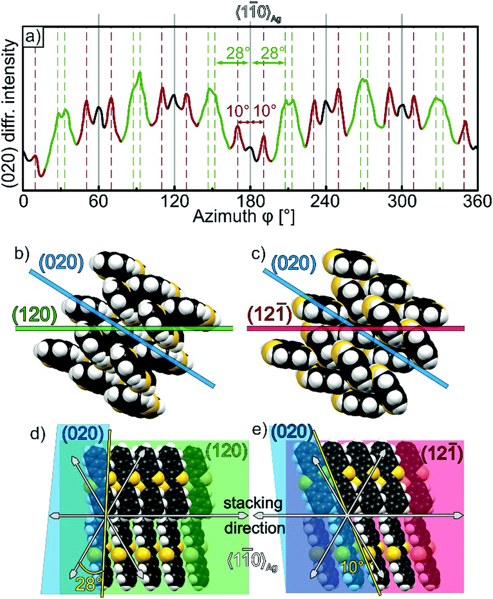 | ||
| Fig. 5 (a) Azimuthal scan of the (020)DNTT reflection intensity recorded for a 100 nm thick DNTT film grown on a Ag(111) substrate that had been exposed before to air. The grey solid lines indicate the positions of the 〈10〉Ag azimuth directions. Panels (b) and (c) show side views ((001) plane) of both observed out-of-plane fiber directions (120) (green) and (12) (red), together with the orientation of the (020) plane (blue) used for the in-plane analysis. Panels (d) and (e) depict the corresponding top views of both fiber orientations where the intersection lines with the (020)DNTT plane are shown as yellow line, which yields characteristic angles of 28° and 10° with respect to the 〈10〉Ag azimuth. | ||
Complementarily to the XRD measurements polarization-resolved optical microscopy was used to characterize the azimuthal distribution of the DNTT fibers and their homogeneity. This analysis is illustrated by the example of a 40 nm DNTT film grown at 340 K onto a Ag(111) surface that was first exposed to air. The corresponding unpolarized optical micrograph is depicted in Fig. 6a and shows elongated fibers running exclusively along the 〈10〉Ag azimuth directions. For the polarization analysis a series of micrographs was recorded with linearly polarized light, wherein the polarization direction was varied. As a next step the intensity of each pixel was analyzed and the polarization angle of the maximal intensity is represented in a false color plot as shown in Fig. 6b, where the color code defines the polarization angle (cf. inset). The observed polarization contrast is caused by a distinct absorption anisotropy of the fibers. As shown in previous work,41 DNTT solids exhibit the main absorption band in the visible range around 2.75 eV (≙580 nm) due to an excitonic excitation. The corresponding transition dipole (TDM) moment is essentially given by the TDM of the lowest energy transition in DNTT molecules, which is oriented along the long axis of the naphthalene units (as depicted in Fig. 6d). Since all molecules in the solid are stacked with their long axis nearly perpendicular to the stacking direction, resp. long axis of the fibers, of the (120)- and (12)-oriented fibers (cf.Fig. 6d), these do not absorb light if the E-vector of the illuminating light is oriented along the fiber direction (i.e. perpendicular to the TDM) and thus appear brightest in that case. The distinct fiber orientation is also evident by the polar histogram shown in Fig. 6c where all pixels with the same polarization angle of maximum intensity are summed up and plotted as a function of the azimuthal polarization. While this polarization analysis map in Fig. 6b clearly reflects the distinct azimuthal distribution of the fibers, it also provides information about the homogeneity of the molecular arrangement within the fibers when considering the signal broadness observed in this evaluation. This shows that despite a uniform molecular alignment for the individual azimuthally oriented fibers, they reveal some inhomogeneity along the fibers and sometimes appear broken.
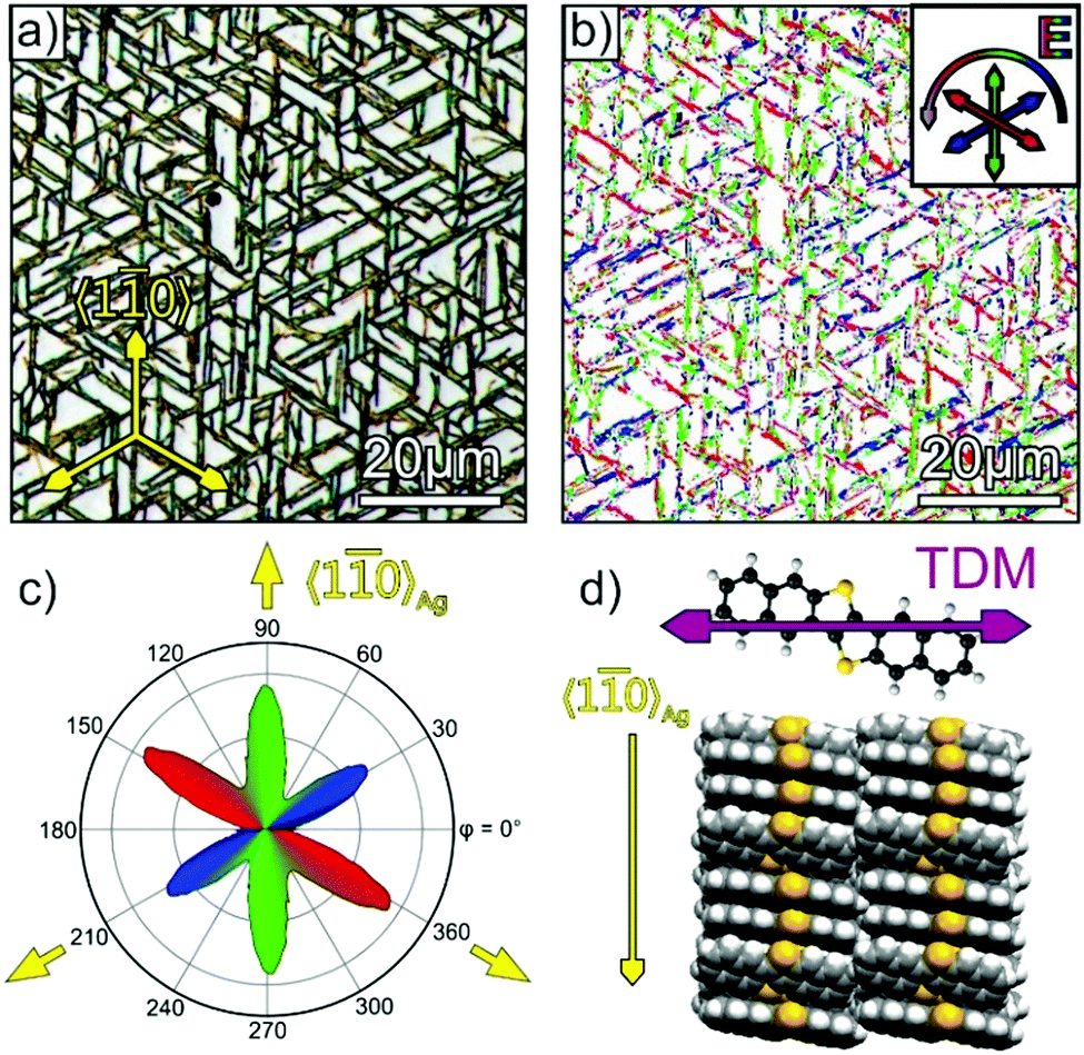 | ||
| Fig. 6 (a) Optical micrograph of a DNTT/Ag(111) film with a nominal thickness of 40 nm deposited at 340 K. (b) Polarization analysis map of image (a), where colors represent the polarization angle of maximal pixel intensity. The polar plot in (c) represents a histogram of the occurrence of pixels in (b) with a certain polarization angle. Panel (d) shows the TDM of the lowest energetic excitation in DNTT,41 together with the molecular arrangement adopted in a (120)-oriented fiber. | ||
Conclusions and outlook
Understanding interface structures and initial nucleation phenomena is of key importance for a structural optimization of functional organic films. Using the example of the high-performant organic semiconductor DNTT, we demonstrate that the morphology of such organic films grown on noble metal substrates is distinctly affected by steps, as they govern the azimuthal alignment of molecules in the seeding monolayer and the subsequently formed crystalline fibers.While using the regular step array of a vicinal surface enables a mesoscopic alignment of the DNTT fibers as demonstrated for the Au(998) substrate, this approach cannot be scaled up because of limitations in preparing such templates with large surfaces. Yet, we were able to develop a strategy to reliably suppress this defect-driven, parasitic fiber growth, which competes with the intrinsic epitaxial alignment of DNTT adopted on the undisturbed, densely packed (111) surface and, as a result, limits the dimensions of the fibers. Combining X-ray diffraction, AFM and polarization resolved optical microscopy we show that first exposing the Ag(111) substrate to oxygen causes a selective adsorption at steps and thereby deactivates the step induced nucleation. The subsequent DNTT film growth results in the formation of largely enhanced crystalline fibers extending over more than 100 μm that are exclusively oriented along the 〈10〉Ag azimuth directions which validates our approach.
Since highly ordered and very smooth (111)-oriented noble metal surfaces can be easily and reliably prepared by epitaxial film growth on mica supports, this approach can be scaled up also to larger surfaces. In a more general scheme, these substrates may serve as template for the fiber growth, while the fibers can be later transferred onto the target substrate. We envision that the presently introduced approach of improving organic film ordering by suppression of unwanted nucleation by initial selective adsorption of small molecules at steps can also be applied to other molecular systems. Therefore, this approach should be helpful for various hybrid systems where structural control on a mesoscopic scale is required.
Experimental section
Sample preparation
For the present study, various metal substrates have been examined. Ag(111) and Au(998) single crystals (MaTeck GmbH) were used as well as Au(111) and Ag(111) samples consisting of 100–200 nm metal films that were epitaxially grown under high vacuum conditions onto freshly cleaved and carefully degassed mica substrates, as described elsewhere in detail.30 As shown in previous work, the latter substrates are remarkably smooth and exhibit highly ordered (111) surfaces consisting of atomically flat terraces with widths of more than 100 nm as well as densely packed 〈10〉-oriented step-edges extending over several microns.31 Prior to each organic film deposition, the metal surfaces were cleaned in situ by repeated cycles of Ar+ sputtering (Eion ≈ 800 eV) and annealing (≈730–750 K) until a sharp low energy electron diffraction (LEED) pattern with a low background signal was observed and no traces of contaminations were found by STM. The DNTT (Sigma-Aldrich, purity: 99%) thin films were prepared under ultra-high vacuum (UHV) conditions by organic molecular beam deposition (OMBD) from aluminum crucibles of a resistively heated Knudsen cell. The deposition rate (typical ≈ 4 Å min−1) was monitored by a quartz crystal microbalance (QCM) and the metal substrates were kept at 340 K during deposition. Additional DNTT films were grown onto silver substrates which had been exposed to oxygen (Praxair, purity 6.0) dosages between 100 and 2000 L (1 L ≡ 1.33 × 10⁻⁶ mbar s) by backfilling the UHV chamber to a pressure of 1 × 10⁻⁶ mbar.
Film characterization
The microstructural order of the DNTT monolayer films was characterized in situ by means of STM (OMICRON VT STM XA), operated in constant current mode and using etched tungsten tips. To avoid admolecule diffusion, the STM data were acquired at sample temperatures of about 110 K. Complementarily, the film morphology was characterized by AFM (Agilent SPM 5500), operated under ambient conditions in tapping mode using MikroMasch cantilevers with a resonance frequency of about 325 kHz and a spring constant of 40 N m−1. All AFM and STM data were visualized and evaluated using the SPIP 5.1.5 (Image Metrology) software. X-ray diffraction (XRD) was employed to analyze the crystalline structure of (multilayer) films, using a Bruker D8 Discover diffractometer with monochromatized Cu Kα radiation (λ = 1.542 Å) and a LynxEye silicon strip detector. Additional information on the morphology and azimuthal orientation of the molecular fibers was obtained by polarized optical microscopy (Nikon Eclipse LV-FMA) operated in epi-illumination. The optical micrographs were recorded using linearly polarized light for illumination and rotating the azimuthal polarization orientation in steps of 5°. Due to the optical anisotropy of DNTT molecules also crystalline films exhibit a notable anisotropy. Following a method described in ref. 32, the angular distribution of DNTT fibers was analyzed by pixelwise evaluation of the polarization angle that yields the largest intensity.Conflicts of interest
There are no conflicts to declare.Acknowledgements
The authors acknowledge support by the Deutsche Forschungsgemeinschaft (Grant No. SFB 1083, TP A2) and Dr F. Balzer (Mads Clausen Institute, University of Southern Denmark) for assistance with the polarization analysis.Notes and references
- D. B. Mitzi, K. Chondroudis and C. R. Kagan, IBM J. Res. Dev., 2001, 44, 29–45 Search PubMed.
- C. Sanchez, P. Belleville, M. Popall and L. Nicole, Chem. Soc. Rev., 2011, 40, 696–753 RSC.
- S. H. Mir, L. A. Nagahara, T. Thundat, P. Mokarian-Tabari, H. Furukawa and A. Khosla, J. Electrochem. Soc., 2018, 165, B3137–B3156 CrossRef CAS.
- D. Käfer, C. Wöll and G. Witte, Appl. Phys. A: Mater. Sci. Process., 2009, 95, 273–284 CrossRef.
- S. A. Burke, J. M. Topple and P. Grütter, J. Phys.: Condens. Matter, 2009, 21, 423101 CrossRef CAS PubMed.
- G. Hlawacek and C. Teichert, J. Phys.: Condens. Matter, 2013, 25, 143202 CrossRef PubMed.
- M. Kothe, F. Widdascheck and G. Witte, J. Phys. Chem. C, 2019, 123, 6097–6106 CrossRef CAS.
- H. Yanagi and S. Okamoto, Appl. Phys. Lett., 1997, 71, 2563–2565 CrossRef CAS.
- H. Yanagi and S. Okamoto, Appl. Phys. Lett., 1999, 75, 187–189 CrossRef CAS.
- F. Balzer, V. G. Bordo, A. C. Simonsen and H. G. Rubahn, Phys. Rev. B: Condens. Matter Mater. Phys., 2003, 67, 115408 CrossRef.
- G. Koller, S. Berkebile, J. R. Krenn, G. Tzvetkov, G. Hlawacek, O. Lengyel, F. P. Netzer, C. Teichert, R. Resel and M. G. Ramsey, Adv. Mater., 2004, 16, 2159–2162 CrossRef CAS.
- F. Balzer and H. G. Rubahn, Adv. Funct. Mater., 2005, 15, 17–24 CrossRef CAS.
- F. Balzer, M. Schiek, A. Lützen and H. G. Rubahn, Chem. Mater., 2009, 21, 4759–4767 CrossRef CAS.
- S. Blumstengel, H. Glowatzki, S. Sadofev, N. Koch, S. Kowarik, J. P. Rabe and F. Henneberger, Phys. Chem. Chem. Phys., 2010, 12(37), 11642–11646 RSC.
- T. Breuer and G. Witte, Phys. Rev. B: Condens. Matter Mater. Phys., 2011, 83, 155428 CrossRef.
- C. Simbrunner, D. Mabok, G. Hernandez-Sosa, M. Oehzelt, T. Djuric, R. Resel, L. Romaner, P. Puschnig, C. Ambrosch-Draxl, I. Salzmann, G. Schwabegger, I. Watzinger and H. Sitter, J. Am. Chem. Soc., 2011, 133, 3056–3062 CrossRef CAS PubMed.
- J. Novak, M. Oehzelt, S. Berkebile, M. Koini, T. Ules, G. Koller, T. Haber, R. Resel and M. G. Ramsey, Phys. Chem. Chem. Phys., 2011, 13, 14675–14684 RSC.
- N. Hiroshiba, R. Hayakawa and Y. Wakayama, Org. Electron., 2019, 74, 33–36 CrossRef CAS.
- J. Kjelstrup-Hansen, C. Simbrunner and H. G. Rubahn, Rep. Prog. Phys., 2013, 76, 126502 CrossRef PubMed.
- A. Matkovic, J. Genser, D. Lüftner, M. Kratzer, R. Gajic, P. Puschnig and C. Teichert, Sci. Rep., 2016, 6, 38519 CrossRef CAS PubMed.
- S. Lukas, G. Witte and Ch. Wöll, Phys. Rev. Lett., 2002, 88, 028301 CrossRef CAS PubMed.
- P. Guaino, D. Carty, G. Hughes, O. McDonald and A. A. Cafolla, Appl. Phys. Lett., 2004, 85, 2777–2779 CrossRef CAS.
- S. Söhnchen, S. Lukas and G. Witte, J. Chem. Phys., 2004, 121, 525–534 CrossRef PubMed.
- J. Götzen, S. Lukas, A. Birkner and G. Witte, Surf. Sci., 2011, 605, 577–581 CrossRef.
- S. Müllegger, I. Salzmann, R. Resel, G. Hlawacek, C. Teichert and A. Winkler, J. Chem. Phys., 2004, 121, 2272 CrossRef PubMed.
- D. Käfer, L. Ruppel and G. Witte, Phys. Rev. B: Condens. Matter Mater. Phys., 2007, 75, 085309 CrossRef.
- G. Hlawaceka, C. Teicherta, S. Müllegger, R. Resel and A. Winkler, Synth. Met., 2004, 146, 383–386 CrossRef.
- U. Zschieschang, F. Ante, T. Yamamoto, K. Takimiya, H. Kuwabara, M. Ikeda, T. Sekitani, T. Someya, K. Kern and H. Klauk, Adv. Mater., 2010, 22, 982–985 CrossRef CAS PubMed.
- M. Dreher, D. Bischof, F. Widdascheck, A. Huttner, T. Breuer and G. Witte, Adv. Mater. Interfaces, 2018, 5, 1800920 CrossRef.
- D. Käfer, G. Witte, P. Cyganik, A. Terfort and C. Wöll, J. Am. Chem. Soc., 2006, 128, 1723–1732 CrossRef PubMed.
- L. Fernandez, S. Thussing, A. Mänz, J. Sundermeyer, G. Witte and P. Jakob, Phys. Chem. Chem. Phys., 2017, 19, 2495–2502 RSC.
- F. Balzer and M. Schiek, Springer Ser. Mater. Sci., 2015, 217, 151–176 CAS.
- Y. Hasegawa, Y. Yamada, T. Hosokai, K. R. Koswattage, M. Yano, Y. Wakayama and M. Sasaki, J. Phys. Chem. C, 2016, 120, 21536–21542 CrossRef CAS.
- J. Kröger, N. Néel, H. Jensen, R. Berndt, R. Rurali and N. Lorente, J. Phys.: Condens. Matter, 2006, 18, S51–S66 CrossRef.
- J. Wang, I. Kaur, B. Diaconescu, J. M. Tang, G. P. Miller and K. Pohl, ACS Nano, 2011, 5, 1792–1797 CrossRef CAS PubMed.
- S. Lukas, S. Vollmer, G. Witte and C. Wöll, J. Chem. Phys., 2001, 114, 10123–10130 CrossRef CAS.
- T. L. Einstein, Appl. Phys. A: Mater. Sci. Process., 2007, 87, 375–384 CrossRef CAS.
- Q. Chen and N. V. Richardson, Prog. Surf. Sci., 2003, 73, 59–77 CrossRef CAS.
- F. Buatier de Mongeot, U. Valbusa and M. Rocca, Surf. Sci., 1995, 339(3), 291–296 CrossRef CAS.
- V. I. Bukhtiyarov, V. V. Kaichev and I. P. Prosvirin, J. Chem. Phys., 1999, 111, 2169–2175 CrossRef CAS.
- Y. Ishino, K. Miyata, T. Sugimoto, K. Watanabe, Y. Matsumoto, T. Uemura and J. Takeya, Phys. Chem. Chem. Phys., 2014, 16, 7501–7512 RSC.
Footnote |
| † Electronic supplementary information (ESI) available: Additional XRD, LEED and AFM data as well optical micrographs. See DOI: 10.1039/c9nh00422j |
| This journal is © The Royal Society of Chemistry 2019 |