
Incorporating mixed cations in quasi-2D perovskites for high-performance and flexible photodetectors†
Ruoting
Dong
a,
Changyong
Lan
 ab,
Fangzhou
Li
a,
SenPo
Yip
acd and
Johnny C.
Ho
*acde
ab,
Fangzhou
Li
a,
SenPo
Yip
acd and
Johnny C.
Ho
*acde
aDepartment of Materials Science and Engineering, City University of Hong Kong, Kowloon, Hong Kong. E-mail: johnnyho@cityu.edu.hk
bSchool of Optoelectronic Science and Engineering, University of Electronic Science and Technology of China, Chengdu 610054, P. R. China
cState Key Laboratory of Terahertz and Millimeter Waves, City University of Hong Kong, Kowloon, Hong Kong
dShenzhen Research Institute, City University of Hong Kong, Shenzhen 518057, P. R. China
eCentre for Functional Photonics, City University of Hong Kong, Kowloon, Hong Kong
First published on 15th July 2019
Abstract
Recently, due to the excellent and tunable optoelectrical properties, quasi-two-dimensional (quasi-2D) layered perovskites have attracted tremendous attention for next-generation optoelectronic devices. However, fabricating high-quality 2D perovskite films, especially with low trap density, is still a challenge. Here, we successfully incorporate different concentrations of FA and Cs cations (i.e. mixed cations) into the quasi-2D perovskites of (iBA)2(MA)3Pb4I13 (FA = formamidinium; iBA = iso-butylamine; MA = methylamine) to modulate their thin film qualities, improving their subsequently fabricated device performances. When configured into photodetectors on rigid substrates, the optimal mixed cation-incorporated (iBA)2(MA)3Pb4I13 perovskites exhibit impressive photodetection properties, which are comparable or even better than those of other 2D perovskite-based photodetectors previously reported. Once fabricated as a flexible photodetector on polyimide, the quasi-2D perovskite device demonstrates further improved performances, yielding a good responsivity of 400 mA W−1, a high detectivity up to 1.68 × 10¹² Jones and fast response speeds (rise and decay time constants of 43 and 22 ms, respectively) under 532 nm illumination. Importantly, the obtained devices possess excellent mechanical flexibility and durability with photocurrent maintaining 82% of the initial value even after 9000 bending cycles. This work can provide valuable design guidelines of 2D perovskites to obtain high-performance flexible photodetectors for next-generation optoelectronics.
New conceptsDue to their unique properties, three-dimensional (3D) organic–inorganic halide perovskites have attracted wide attention recently for various optoelectronic devices. However, the intrinsic instability of 3D perovskites against moisture restricts their use for practical applications. Great efforts have then been devoted to developing quasi-two-dimensional (qusai-2D) perovskites due to their much better stability. But their device performances are still poor as compared with their 3D counterparts due to inefficient charge transport, which results from the large insulating organic cations separating the inorganic metal halide layers. In this paper, for the first time, an exceptionally simple synthetic method is developed to incorporate a unique combination of formamidinium (FA) and cesium (Cs) mixed cations with well-controlled composition into (iBA)2(MA)3Pb4I13 (BA = iso-butylamine and MA = methylamine) to achieve quasi-2D perovskite films with remarkably enhanced film quality. This optimized mixed cation incorporation can not only improve the charge transport among the inorganic metal halide layers, but also enable excellent operational stability and performance enhancement in photodetection, especially for flexible photodetectors with high responsivities, short response times and good mechanical robustness. Overall, incorporating these exclusive mixed cations provides valuable design guidelines and new insights into stable perovskite materials for high-performance flexible photodetectors. |
Introduction
In the past decade, three-dimensional (3D) perovskites have been widely explored as active materials for numerous optoelectronic devices, such as solar cells,1,2 photodetectors,3–6 and light emitting diodes.7–9 In particular, flexible photodetectors (PDs), converting light into electrical signals on mechanically bendable platforms which can be attached onto any arbitrary surface, are essential device components in many advanced technological areas of optical communication, automatic control, imaging and biochemical sensors, etc.10 Utilizing 3D hybrid organic–inorganic perovskites (e.g. MAPbX3; MA = CH3NH3; X = Cl, Br, and I), these fabricated flexible photodetectors are demonstrated with good device performance in terms of excellent light absorption, high charge carrier mobility and robust mechanical flexibility.4,11–13 However, the intrinsic instability of conventional 3D perovskites against ambient moisture greatly restricts their use in high-performance photodetectors as they cannot transduce the signal repeatedly over long periods of duration during operation. In this regard, it is urgently required to resolve the instability issue of 3D perovskites prior to their practical deployment for optoelectronics.10,14At the same time, there is another type of perovskite material proved with much enhanced stability, namely quasi-two-dimensional (quasi-2D) layered perovskites (also known as Ruddlesden–Popper phases), which have a crystal structure consisting of 2D perovskite slabs interleaved with cations.15 They generally adopt a chemical formula of L2An−1PbnX3n+1, where L is a large size or long-chain organic cation, A is a regular cation, and X is a halide.16,17 The variable n is an integer, indicating the number of metal halide octahedral layers between the two L cation layers.18,19 The stacking layer contains an extended network of corner-sharing metal halide octahedra (PbX6) and two layers of organic cations capping both sides of the inorganic layer to balance the charge. Because of the stronger interaction between the (PbX6) octahedra and organic molecules, as well as the hydrophobicity of L cations, these 2D perovskites present prominent resistance to moisture degradation as compared with other perovskite materials.20,21 Furthermore, these quasi-2D perovskites, typically derived from the initial 3D perovskite motifs interleaved by large organic cations, also exhibit abundant and tunable optoelectronic properties, being advantageous for utilization in photodetectors.22 For instance, Peng and co-workers developed the first photodetector based on individual BA2PbBr4 (BA = C4H9NH3) microplatelets, which was built with the protection and top contact of graphene films, displaying excellent photoresponsivity.23 Also, Huang et al. reported photoconductors using (BA)2MAn−1PbnI3n+1 (n = 1, 2, and 3) that yielded a tunable photoresponse and a short response time.24 Although there have been a number of publications focused on 2D perovskite materials and their associated photodetectors, until now, almost all devices were fabricated on rigid substrates, and very few are configured as mechanically flexible photodetectors.10,25,26 It should be noted that since 2D RP perovskites are van der Waals layered materials, the stress created inside the materials during bending can be easily released. As a result, these materials are highly suitable for flexible devices, especially flexible photodetectors.
Nevertheless, the device performance of quasi-2D perovskite photodetectors is relatively poor as compared with that of their 3D perovskite counterparts due to the inefficient charge transport, which results from the large insulating organic cations separating the inorganic metal halide layers.27 Previous studies reveal that the quality of 2D perovskite films and their fabricated device performance can be improved through different approaches, including hot casting, additive-assisted and solvent engineering, and adopting shorter spacer ligands, etc.25,27–29 Despite these successes, fabricating 2D perovskite films with high quality, especially low trap density, is still a challenge. Among all these approaches, composition engineering has been shown as one of the effective routes to tackle the issues of achieving high-quality perovskite films.30 In view of the perovskite components, cations, especially FA (FA = HC(NH2)2) and Cs, play an important role in enhancing the performance of perovskite based devices. To be specific, Zhou et al. revealed that appropriate FA incorporation in 2D BA2(MA)3Pb4I13 can effectively control the perovskite crystallization kinetics, which reduces the non-radiative recombination centers to acquire high-quality films with limited non-orientated phases.31 Liu et al. acquired Cs doping into 2D BA2(MA)3Pb4I13 to modify the perovskite film quality for enriched properties.32 Etgar and co-workers extended to the 2D/3D perovskite studies, where Cs is introduced into the lattice matrix as an additional small cation to MA in order to improve the photovoltaic performance of subsequently fabricated devices.33 Notably, it has been suggested that the use of all three cations of Cs, MA and FA in 3D perovskites can provide additional versatility in fine-tuning the film characteristics.34 Investigation of mixed cations in low-dimensional perovskites is thus adequately worthy for inquiry regarding the optimization of their morphology, optical properties and successive device performance.
In this work, we develop successfully a simple but effective strategy to introduce an FA-Cs mixture with well-controlled composition to achieve high-quality quasi-2D layered perovskite films by using the conventional spin-coating technique. Upon configuring as photodetectors on rigid substrates, the optimal FA- and Cs-doped (iBA)2(MA)3Pb4I13 perovskites give much enhanced photodetection properties as compared with those of pristine counterparts under 532 nm illumination. When these mixed cation (i.e. FA and Cs cations) incorporated 2D perovskites are fabricated as flexible photodetectors on polyimide, they exhibit excellent device performance with a good responsivity of 400 mA W−1, a high detectivity up to 1.68 × 10¹² Jones, a large on–off ratio of 720 and fast response speeds (rise and decay time constants of 43 and 22 ms, respectively). More importantly, these devices possess robust mechanical characteristics and their photocurrent presents a decay of only 18% of its initial value even after 9000 bending cycles. This work can evidently provide a valuable design guideline of 2D perovskites to obtain high-performance flexible photodetectors for next-generation optoelectronics devices.
Results and discussion
Here, the quasi-2D (iBA)2(MA)3Pb4I13 perovskite precursor solutions are synthesized with a stoichiometric reaction among PbI2, C4H9NH2, HI and MAI at a specific ratio of 4![[thin space (1/6-em)]](https://www.rsc.org/images/entities/char_2009.gif) :2:2:3 in DMF. In order to obtain the family of (iBA)2(MA1−xFAx)3Pb4I13 (x = 0, 0.20, 0.40, 0.60), a part of MAI is purposely replaced with FAI in the precursor solution (Fig. 1a). With the aim to simplify the expression of the chemical formula, we use FA0, FA0.20, FA0.40, FA0.60 to represent (iBA)2(MA1−xFAx)3Pb4I13 with the value of x = 0, 0.20, 0.40, and 0.60, respectively. As shown in Fig. 1c–f, atomic force microscopy (AFM) is employed to reveal the morphology difference among fabricated perovskite films with different FA contents. It is clear that the pristine FA0 film features full film coverage without any obvious pinholes (Fig. 1c). When 20% FA is introduced, the film begins to become rougher but with less cracks (Fig. 1d). Once the FA content hits 40%, the film exhibits a significant surface roughness with the presence of observable pin-holes, which is probably attributed to the release of MAI during the film-forming process (Fig. 1e). When the FA composite increases further to 60%, the film starts to turn into uneven, being composed of inhomogeneous grains, which implies the imperfect crystallization in the absence of process optimization (Fig. 1f). The introduction of FA content can evidently modulate the morphology of quasi-2D perovskite films. This surface morphology evolution of the obtained films is perfectly consistent with the SEM results as depicted in Fig. S1 (ESI†). Overall, upon the addition of FA, the films become rougher with the root mean square (RMS) surface roughness values increasing from 1.20 nm (FA = 0) to 10.80 nm (FA = 0.20), 9.37 nm (FA = 0.40) and eventually 27.9 nm (FA = 0.60), accordingly.
:2:2:3 in DMF. In order to obtain the family of (iBA)2(MA1−xFAx)3Pb4I13 (x = 0, 0.20, 0.40, 0.60), a part of MAI is purposely replaced with FAI in the precursor solution (Fig. 1a). With the aim to simplify the expression of the chemical formula, we use FA0, FA0.20, FA0.40, FA0.60 to represent (iBA)2(MA1−xFAx)3Pb4I13 with the value of x = 0, 0.20, 0.40, and 0.60, respectively. As shown in Fig. 1c–f, atomic force microscopy (AFM) is employed to reveal the morphology difference among fabricated perovskite films with different FA contents. It is clear that the pristine FA0 film features full film coverage without any obvious pinholes (Fig. 1c). When 20% FA is introduced, the film begins to become rougher but with less cracks (Fig. 1d). Once the FA content hits 40%, the film exhibits a significant surface roughness with the presence of observable pin-holes, which is probably attributed to the release of MAI during the film-forming process (Fig. 1e). When the FA composite increases further to 60%, the film starts to turn into uneven, being composed of inhomogeneous grains, which implies the imperfect crystallization in the absence of process optimization (Fig. 1f). The introduction of FA content can evidently modulate the morphology of quasi-2D perovskite films. This surface morphology evolution of the obtained films is perfectly consistent with the SEM results as depicted in Fig. S1 (ESI†). Overall, upon the addition of FA, the films become rougher with the root mean square (RMS) surface roughness values increasing from 1.20 nm (FA = 0) to 10.80 nm (FA = 0.20), 9.37 nm (FA = 0.40) and eventually 27.9 nm (FA = 0.60), accordingly.
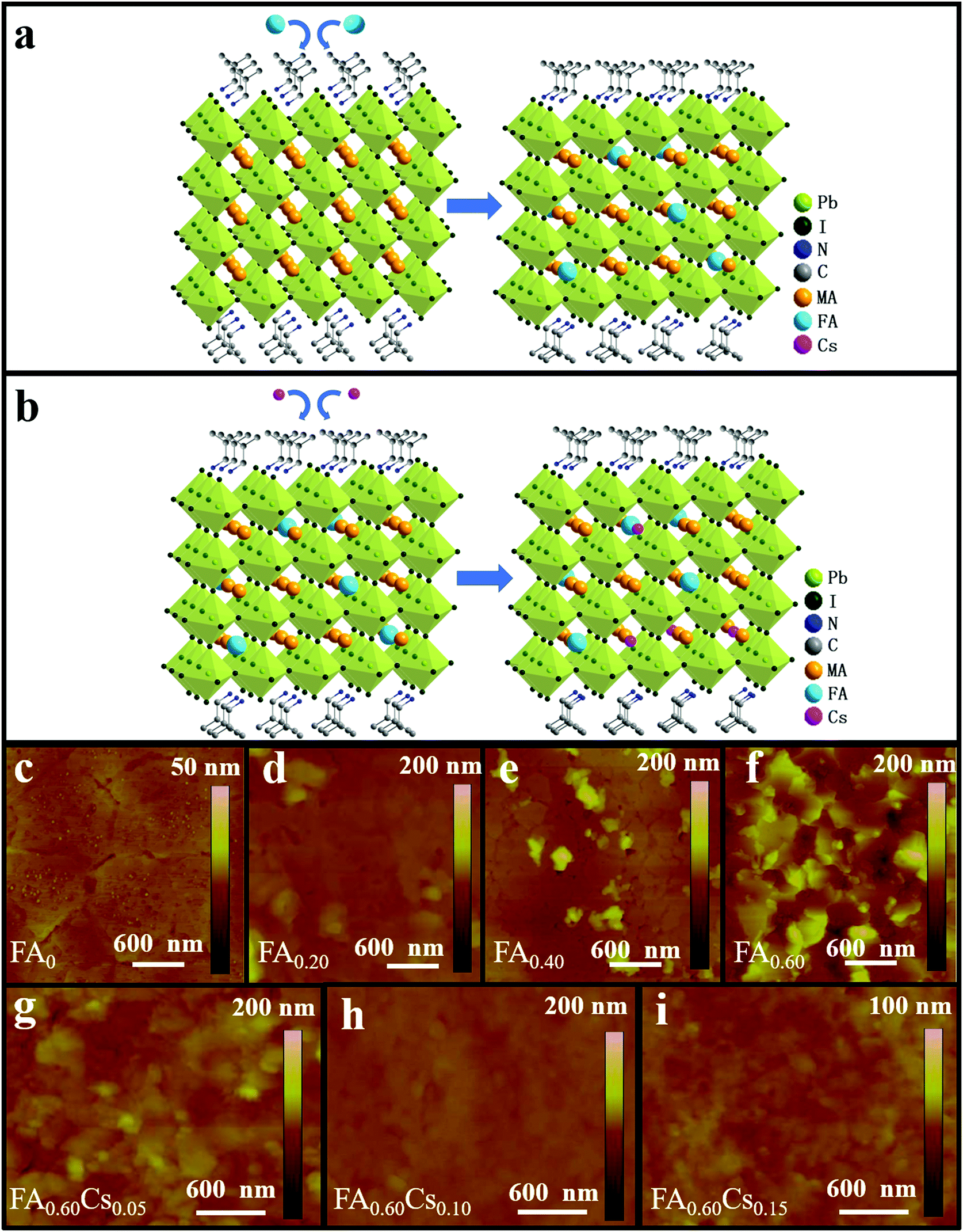 | ||
| Fig. 1 Schematic illustration of the crystal structure of (a) FA-incorporated layered perovskite materials with the formula of (iBA)2(MA1−xFAx)3Pb4I13 and (b) mixed cation (FA and Cs) incorporated layered perovskite materials with the formula of (iBA)2((MA0.40FA0.60)1−yCsy)3Pb4I13. AFM images of the samples of (c)–(f) FAx (x = 0, 0.20, 0.40 and 0.60) and (g)–(i) FA0.60Csy (y = 0, 0.05, 0.10 and 0.15). | ||
To assess the effect of different FA contents on light absorption characteristics of the fabricated 2D perovskite samples, the optical absorption measurement is performed with the spectra presented in Fig. S2a (ESI†). There are three absorption peaks (at around 550–650 nm) observed for all samples, which are in perfect agreement with previous reports with the peaks originated from excitonic absorptions.27 This observation indicates that the absorption characteristic is not changed by the partial substitution of MA with FA. It is worth mentioning that the Tauc plot cannot be used to determine the band gap of quasi-2D perovskites due to the difference of the joint density states of 3D and 2D materials.35 Besides, it is observed that when the FA content is 60%, the perovskite film demonstrates the largest optical absorbance with the same film thickness of around 400 nm as compared with other samples, which may be attributed to the better light capturing and scattering capability of its rough morphology. With these results, we speculate that the FA0.60 perovskite film holds great potential in achieving high-performance photodetectors. Therefore, we decide to perform Cs doping into the 2D FA0.60 sample to further modify the perovskite with mixed cations (i.e. FA and Cs) for optimized material properties and device performance in subsequent photodetector fabrication (Fig. 1b). The chemical formula of (iBA)2((MA0.4FA0.6)1−yCsy)3Pb4I13 perovskites is then simplified into the expression of FA0.60Cs0.05, FA0.60Cs0.10 and FA0.60Cs0.15 with the Cs doping content of 0.05, 0.10 and 0.15 respectively. SEM and AFM measurements are also employed to study the morphology of the family of (iBA)2((MA0.40FA0.60)1−yCsy)3Pb4I13 perovskite films. As shown in Fig. 1g–i and Fig. S1e–g (ESI†), after introducing the Cs component, all three Cs-based perovskite films display compact and uniform morphology without any observable pinholes, which can be attributed to the fact that the incorporation of Cs promotes the formation of dense and uniform films. When the Cs content is 10%, the sample appears as a smooth film with reduced surface roughness and significantly decreased grain boundaries (Fig. 1h) as compared with the ones of both samples of 5% and 15% Cs (Fig. 1g and i). The RMS surface roughness of FA0.60Cs0.05, FA0.60Cs0.10 and FA0.6Cs0.15 are found to be 10.7, 2.21 and 2.89 nm, respectively, which confirms the superior film conformality of FA0.60Cs0.10. Also, the optical absorption spectra of all mixed cation incorporated perovskite films are obtained and presented in Fig. S2b (ESI†). Among different samples, FA0.60Cs0.10 exhibits the best light harvesting ability throughout the entire measurement wavelength range. This indicates that the incorporation of an appropriate amount of Cs can improve optical absorption. It is well-known that the smooth, compact and uniform surface morphology with fewer grain boundaries of the film can result in the relieved charge recombination and the enhanced photoelectric properties.36,37 Therefore, it is highly anticipated that the perovskite film of FA0.60Cs0.10 is of great potential in fabricating high-performance optoelectronic devices.
Moreover, X-ray diffraction (XRD) patterns are also acquired to obtain further insights into the crystal structure of all obtained perovskite films. All samples give intense characteristic peaks within the 2θ range of 14°–15° and 28°–29° corresponding to the (111) and (220) planes of the perovskite crystal structure (Fig. 2). As the FA content increases from 0 to 60%, the diffraction peaks of the (111) plane display a slight shift to a lower angle, attributed to the larger size of the FA cation with respect to the MA cation and hence the expansion of the 2D perovskite crystal lattice (Fig. S3a, ESI†).31 The same phenomenon can also be observed for the diffraction peaks of the (220) plane (Fig. S3b, ESI†). Notably, a new set of periodic (00k) peaks are also found in the FA0.60 film, which can be assigned to the FA-doped BA2MAPb2I7 (n = 2) 2D perovskite in the FA0.60 film.31 With the increase of the Cs content (from 0 to 15%), the diffraction peaks of (111) and (220) planes present a small shift to the higher angle (Fig. S3c and d, ESI†), which is in good agreement with the smaller size of Cs relative to MA to shrink the crystal lattice.33 In addition, after introducing the Cs component, all films display improved diffraction intensity, especially for the sample of FA0.60Cs0.10 with the strongest diffraction intensities, suggesting the best crystallinity among all samples here. When the full-width at half-maximum (FWHM) of the (220) peaks of FA0.60Csy (y = 0, 0.05, 0.10, 0.15) perovskite films are evaluated, their values are found to be 0.229°, 0.178°, 0.172° and 0.209°, respectively (Fig. S4, ESI†), which correspond to the crystalline size of 35, 45, 47 and 38 nm, accordingly, by applying the Scherrer analysis. It is also noted that the small (00k) peak assigned to the FA-doped BA2MAPb2I7 2D perovskite in the FA0.60 film is not observed, which designates the enhanced phase purity of FA0.60Csy films achieved by the Cs incorporation. All these results reveal that the subsequent Cs incorporation can promote an increase of 2D perovskite crystal size with the FA0.60Cs0.10 film demonstrating the best crystallization.
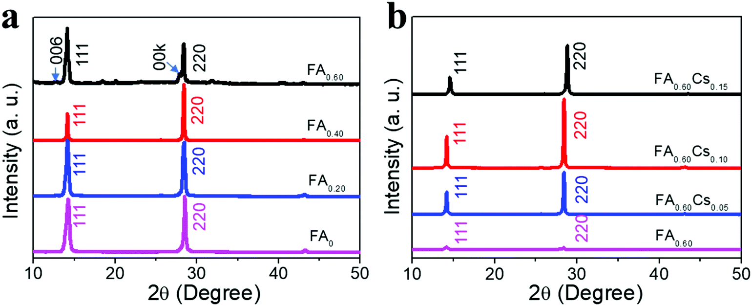 | ||
| Fig. 2 XRD characterization of (a) FAx (x = 0, 0.20, 0.40 and 0.60) and (b) FA0.60Csy (y = 0, 0.05, 0.10 and 0.15) films. | ||
Apart from the surface morphology and crystallinity, photoluminescence (PL) spectra and time-resolved PL (TRPL) decay spectra of all samples are measured to assess their emission and carrier recombination properties. As shown in Fig. 3a, the normalized steady-state PL spectrum of the FA0 perovskite has a prominent emission peak at 641.6 nm, which can be ascribed to the excitonic emission from (iBA)2(MA)3Pb4I13, being similar to the PL spectrum observed for (BA)2(MA)3Pb4I13.19 There is also a very weak emission peak located at 730 nm that can be related to the peak of infinite metal halide octahedral layers (i.e. n = ∞), indicating the presence of only trace amounts of 3D perovskite phases in FA0. In this case, the as-synthesized FA0 perovskite film is found to be relatively pure with only small inclusions of 3D perovskite phases. Additionally, we observe tiny but multiple PL emission peaks at 560–700 nm for samples FA0.20, FA0.40 and FA0.60, being similar to their respective absorption shoulders, which can be ascribed to the formation of multiple perovskite phases with small n values coexisting in the 2D perovskite films (although the nominally prepared samples are intended to have the n values of 4). The main PL emission peak of FA0.20, FA0.40 and FA0.60 comes from the 3D perovskites that is attributable to the special distribution and cascade band alignment of 2D perovskites in the mixed phases.35 This way, the photo-generated electrons would transfer from the small-n to the large-n phases, leading to the main emission peak corresponding to n = ∞.35 It is noted that the 3D perovskite peak is witnessed to give a red-shift from 730 nm for FA0, to 736, 752.6 and 765 nm for FA0.20, FA0.40 and FA0.60, respectively, which associates with the reduced band gap energy (Eg) of FAx perovskites for increasing FA content. After incorporating with the FA component, all the films exhibit longer carrier lifetimes than the pristine FA0 perovskite (Fig. 3b). Among them, the FA0.60 film exhibits the longest lifetime of 144.6 ns, clearly revealing the high film quality there with few defects (Table S1, ESI†). At the same time, the normalized PL spectra of FA0.60Csy are given in Fig. 3c. With the introduction of Cs, there is a slight blue-shift in the PL peak position from 765 nm for FA0.60, to 762.2, 755.8 and 749 nm for FA0.60Cs0.05, FA0.40Cs0.10 and FA0.60Cs0.15, accordingly, which is consistent with the slight shrinkage of the 2D perovskite crystal lattice for increasing Cs content. Distinctive small emission peaks of around 560–700 nm are also observed that are correlated to the 2D quantum wells with small n values. Likewise, the TRPL decay spectra are conducted to investigate the recombination dynamics of the 2D perovskite family of FA0.60Csy (Fig. 3d). It is impressive that the FA0.60Cs0.10 film displays the longest lifetime of 210.5 ns among all samples, which is about 52 times longer than the lifetime of the pristine FA0 perovskite (Table S1, ESI†), indicating its slower recombination characteristics of electrons and holes as well as its potentially better device performance in subsequent studies. It is shown that the incorporation of Cs can further improve the carrier lifetimes of quasi-2D perovskite films. This enhanced lifetime is mainly attributed to the increased film crystallinity through the incorporation of FA and Cs ions.
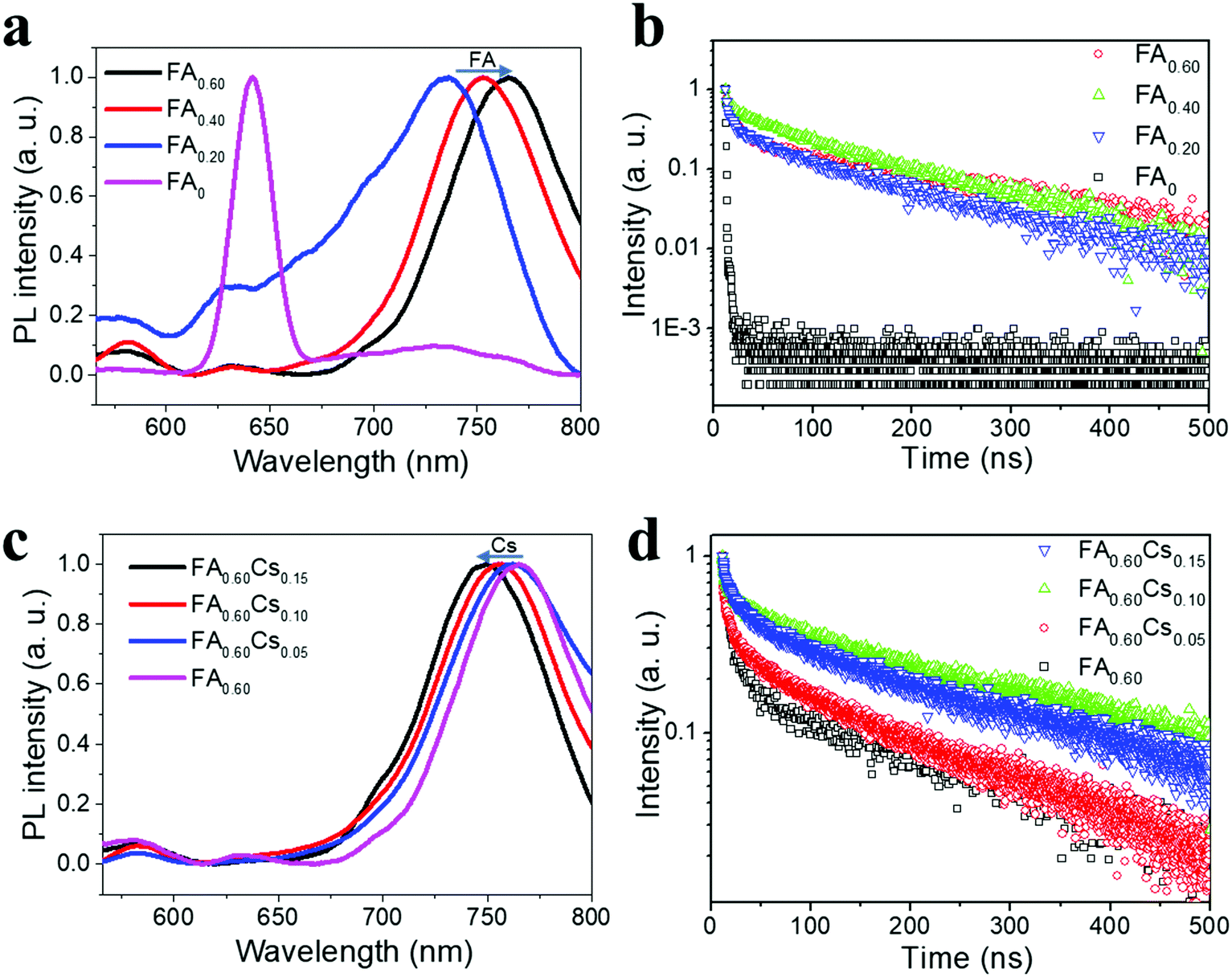 | ||
| Fig. 3 (a) PL spectra, and (b) TRPL spectra of FAx (x = 0, 0.20, 0.40 and 0.60). (c) PL spectra, and (d) time-resolved photoluminescence (TRPL) spectra of FAxCsy (y = 0, 0.05, 0.10 and 0.15). | ||
To shed light on the long-term stability under ambient conditions, the three different 2D FA0.60Csy (y = 0.05, 0.10, 0.15) perovskite films are thoroughly investigated using optical microscopy and XRD under controlled laboratory conditions (i.e. 50% humidity) for up to 30 days. Based on the optical images, there is not any noticeable change observed regarding the film color of these 2D perovskites (Fig. S5a–c insets, ESI†). The XRD patterns of 2D FA0.60Csy films remain unchanged in air for up to 30 days, in which no PbI2 peak is observed demonstrating the good stability of 2D layered perovskite films in high humidity environments. To compare the ambient stability of 3D MAPbI3 and 2D FA0.60Csy, MAPbI3 films are also prepared and stored under the same conditions. Obviously, the MAPbI3 film decomposes gradually and starts to give rise to an XRD signal of PbI2 even only after 4 days of storage (Fig. S5d, ESI†). This result provides compelling evidence of the high degree of stability of 2D FA0.6Csy perovskite films under ambient conditions as compared with the one of MAPbI3, where the enhanced stability can be come from the long and bulky hydrophobic organic groups in the 2D perovskite structure. The impressive air stability of 2D layered perovskite films would make them suitable for various technological applications.
Given the above remarkable enhancement in crystallinity, morphology and optical properties of 2D perovskite thin films with mixed cation incorporation, we set out to investigate their performance limits when they are configured as photodetectors. Fig. 4a inset illustrates the architecture of the device, assembled by depositing two Au electrodes onto the perovskite film. The dependence of photoresponse on the light intensity is first systematically studied for the devices with different FA contents. As shown in the photocurrent–voltage (I–V) characteristics in Fig. S6 (ESI†), all devices give the dark current with a range of 6.28 × 10⁻¹¹–1.18 × 10⁻¹⁰ A at a voltage bias of 1.5 V. Once illuminated using a 532 nm laser, the output current of all devices increases with increasing light intensity, indicating the typical light-sensitive properties of the layered perovskite films. Moreover, the I–V curves present linear dependence on the applied bias for all devices, which suggests the nearly Ohmic contact properties between perovskite thin films and gold electrodes, being beneficial for the collection of photogenerated carriers. In principle, the photocurrent is defined as the current difference between the dark and the light illuminated states. To better understand the photosensing characteristics of these 2D perovskites, the dependence of their photocurrent on the light intensity is carefully measured and presented in Fig. 4a. The measured data can be well-fitted by using the following formula of
| Ip = AΦβ | (1) |
 | (2) |
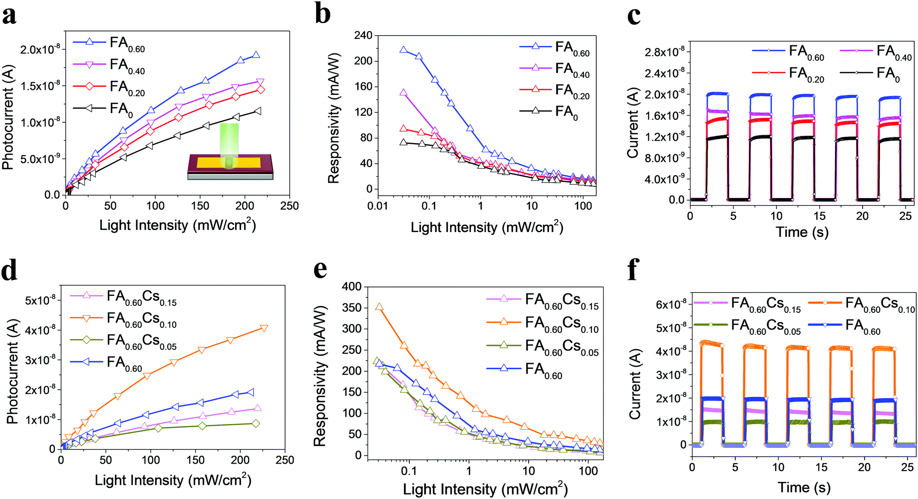 | ||
| Fig. 4 (a) Photocurrent as a function of the light intensity, (b) responsivity as a function of the light intensity, (c) output current as a function of time under modulated incident light of devices configured with FAx (x = 0, 0.20, 0.40 and 0.60) perovskite films. Inset shows the device structure of the photodetector. (d) Photocurrent as a function of the light intensity, (e) responsivity as a function of the light intensity, (f) output current as a function of time under modulated incident light of devices constructed with FA0.60Csy (y = 0, 0.05, 0.10 and 0.15) perovskite films. For (a)–(f), the bias voltage is 1.5 V. The incident light wavelength is 532 nm. The light intensity for (c) and (f) is 0.22 W cm−2. | ||
After that, the optoelectronic performance of both FA- and Cs-incorporated quasi-2D FA0.60Csy perovskite photodetectors are also evaluated. Similarly, the I–V properties of these photodetectors are measured in the dark and under illumination of a 532 nm laser with different intensities (Fig. S8, ESI†). In the dark, all devices have an output current of 1.44 × 10⁻¹⁰–6.72 × 10⁻¹⁰ A at the voltage bias of 1.5 V. Again, the output current is observed to increase with the increasing incident power, which illustrates a typical linear relationship with the bias voltage, indicating an Ohmic-like contact here and thus benefiting the collection of photogenerated carriers. Also, the sub-linear relationship between the device photocurrent and the light intensity is observed, where the β parameters are extracted to be 0.55, 0.67 and 0.71, respectively, for increasing Cs content (Fig. 4d). In order to quantify the photodetector performance, the photoresponsivity of different 2D FA0.60Csy (y = 0, 0.05, 0.10 and 0.15) perovskite devices is carefully assessed as depicted in Fig. 4e. The photoresponsivity (R) is observed to be a decreasing function of the light intensity for all devices, where the FA0.60Cs0.10 sample yields the highest R across the entire measured range with the value of 351 mA W−1. Besides, the photoswitching characteristic of FA0.60Csy samples is as well measured in the dark and under a light intensity of 0.22 W cm−2 (Fig. 4f). The result illustrates that the layer structured perovskites of FA0.60Csy (y = 0.05, 0.10 and 0.15) have reproducible and stable photoresponses, displaying the on/off current ratio of 4.91 × 10², 3.73 × 10² and 1.65 × 10², respectively. The rise and decay time constants of perovskite devices can then be determined as 81/27, 59/24 and 62/35 ms, accordingly, in which all devices demonstrate fast photoresponse characteristics (Fig. S9, ESI†). All these results evidently indicate the excellent photodetection performance of mixed cation incorporated perovskite devices, especially for the FA0.60Cs0.10 film with high crystal quality, which are comparable or even better than those of other 2D perovskite-based photodetectors with a similar metal–semiconductor–metal structure reported to date (Table S2, ESI†).16,23–25,40–46 As a result, the incorporation of both FA and Cs mixed cations is beneficial for the performance improvement of fabricated photodetectors, where the further composition optimization would provide effective modulations over 2D perovskites for utilizations in various high-performance optoelectronic switches and devices. Besides, the operation stability tests are also conducted by tracking the photocurrent changes of the FA0.60Cs0.10 devices stored under humid conditions (50% humidity) over a period of 9 days (Fig. S10, ESI†). The quasi-2D perovskite device retains over 92%, 79% and 67% of its initial photocurrent with the light intensity of 3.93, 2.40 and 0.72 mW cm−2 respectively after 8 days, while they start to exhibit degradation on the 9th day of exposure. In contrast, the MAPbI3 film decomposes to PbI2 even only after 4 days of storage (Fig. S5, ESI†). These findings demonstrate the notably higher operation stability of the quasi-2D perovskite device.
As discussed, since 2D perovskite materials have excellent mechanical flexibility, they are ideal candidates for use in flexible optoelectronics; nevertheless, only a few reports have been focused on flexible 2D perovskite photodetectors until now. In this work, as the FA0.60Cs0.10 film possesses relatively high crystal quality and satisfactory photodetection performance on rigid substrates, it is also valuable to investigate its performance limits for the devices fabricated on mechanically flexible polyimide (PI). Similar to the rigid device, as shown in Fig. S11 (ESI†), the output current of the flexible device rises upon light illumination and further increases with increasing light intensity. Notably, the flexible photodetector has an extremely low dark current of 1.27 × 10⁻¹² A at a voltage bias of 1.5 V as compared to the ones of rigid counterparts. Fabricating quasi-2D perovskite films on a rough PI substrate would introduce more defects on the film surface, which can depress the dark current in flexible photodetectors. This ultra-low dark current confirms that the present 2D FA0.60Cs0.10 perovskite deposited on PI is composed of low carrier density and low thermal emission (recombination) rates, warranting its potential as an efficient light photodetector for very weak optical signals.40Fig. 5a demonstrates the photocurrent and responsivity of the flexible device against the incident light power density. Importantly, the β value is determined to be 0.65 here, exhibiting the sublinear relationship between the photocurrent and the incident power density. At the same time, the responsivity varies with the light intensity, reaching the highest value of 400 mA W−1, which is further improved in contrast with the rigid device. It is observed that the surface of 2D FA0.60Cs0.10 film becomes much rougher (9.50 nm in the RMS surface roughness) as compared with the one (2.21 nm in the RMS surface roughness) fabricated on rigid substrates (Fig. S12, ESI†), where this roughness is believed to be induced by the relatively coarse surface of PI substrates (Fig. S13, ESI†). In this case, the enhanced photoresponsivity of the flexible devices may be attributed to the rough surface morphology of FA0.60Cs0.10 deposited on PI, where this roughness can scatter the incident light, leading to improved light absorption in 2D perovskites.
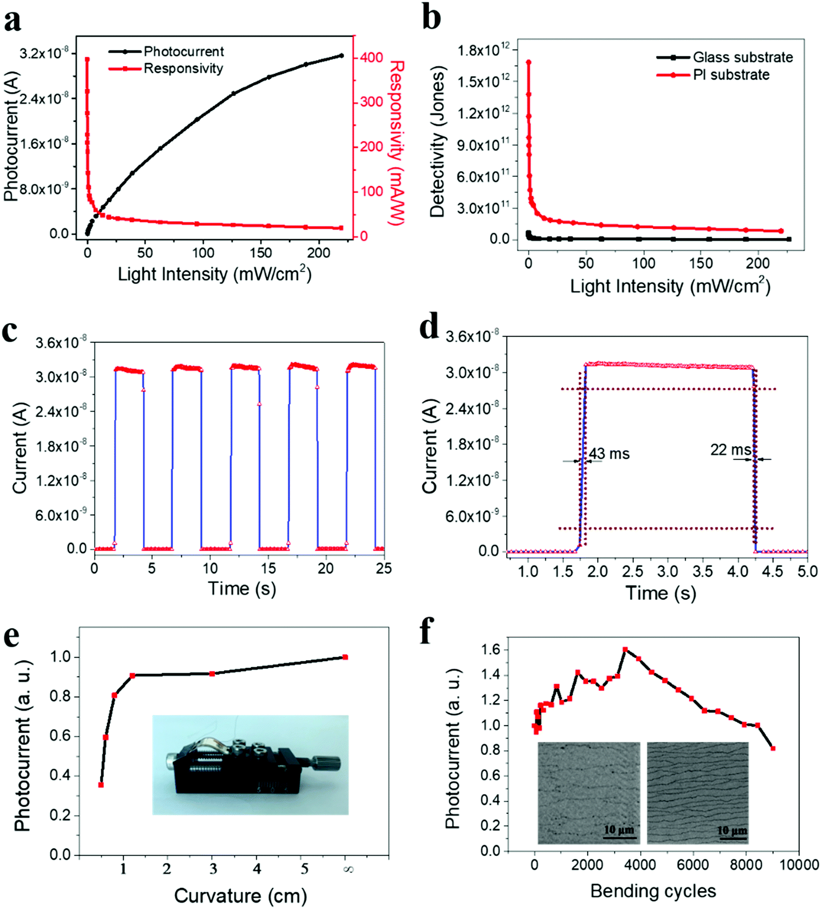 | ||
| Fig. 5 (a) Photocurrent and responsivity of the FA0.60Cs0.10 device fabricated on polyimide (PI) as a function of the illuminated light intensity. (b) Specific detectivity (D*) of the device configured on the rigid glass and flexible PI substrates as a function of the light intensity. (c) Current versus time plot measured under chopped light illumination with a light intensity of 0.22 W cm−2. (d) High-resolution current versus time plot used to determine the rise and decay time constants. (e) Normalized photocurrent versus bending curvature of the flexible device. Inset shows an optical image of the measurement setup under the bending test. (f) Normalized photocurrent versus bending cycles of the flexible device. The device used for the bending tests has a channel length of 83 μm. Inset shows the SEM image of the device electrode (left) and channel (right) after 9000 bending cycles. | ||
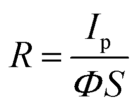
At the same time, detectivity (D*) is always employed to characterize the sensitivity of photodetectors. It is typically related to the total noise, particularly the shot noise coming from the dark current. Its value can be expressed as the following
 | (3) |
For practical utilizations, the device durability is an essential requirement of flexible photodetectors. In order to determine the device stability during mechanical bending, photodetectors with large-size electrodes are fabricated to facilitate the measurements. The corresponding measurement setup is shown in the optical image in Fig. 5e inset. For simplicity, the photocurrent is normalized to the case where no mechanical bending is performed. This way, the normalized photocurrent can be easily measured as a function of the bending curvature (i.e., bending radius) as presented in Fig. 5e. It is observed that the photocurrent decreases with decreasing bending radius, which is commonly seen in conventional 3D perovskite materials.51,52 To further assess the device durability, the stability of the photocurrent is evaluated as a function of the number of bending cycles at a fixed bending radius of 0.5 cm (Fig. 5f). Remarkably, the photocurrent is gradually increasing in the initial period (3420 bending cycles) during the bending test. Such an interesting photocurrent enhancement behavior may be due to the rougher surface caused by the bending, leading to enhanced light absorption arising from the scattering of incident light. When the bending cycles continue, the device photocurrent starts to decrease. Despite this, the measured photocurrent still maintains 82% of its initial value even after 9000 bending cycles (Fig. 5f and Fig. S14a, ESI†). The decrease of the photocurrent can be attributed to the decreased charge transport ability caused by bending. As the 2D perovskite material is a van der Waals layered material, the stacking of different layers can be destroyed by bending (Fig. 5f inset), which degrades the transport path of charge carriers. During the initial bending cycles, this effect may not be strong enough; therefore, the enhanced light absorption dominates the contribution to the photocurrent. While with further bending cycles, this degradation effect becomes more serious, which takes over the contribution to the photocurrent such that the photocurrent decreases eventually. In any case, after the bending test, the photocurrent is still observed to decrease with the decreasing bending radius (Fig. S14b, ESI†) to confirm the operational stability of the device. All these results clearly demonstrate the mechanical flexibility and robustness of the 2D perovskites for high-performance flexible optoelectronic devices.
Conclusions
In summary, we demonstrate the synthesis of quasi-2D layered perovskite films via a one-step solution processing method, in which both FA and Cs cations are introduced into the 2D perovskites to modulate the film quality as well as to improve the performance of subsequently fabricated devices. Upon configuring into photodetectors on rigid substrates, the enhanced photodetection properties of both FA- and Cs-doped (iBA)2(MA)3Pb4I13 perovskites are obtained as compared with those of pristine counterparts under 532 nm illumination. When these mixed cation incorporated quasi-2D perovskites are employed as active channels on mechanically flexible substrates, the photodetection device performance can be further improved, demonstrating a good responsivity of 400 mA W−1, a high detectivity up to 1.68 × 10¹² Jones, a large on–off current ratio of 720 and fast response speeds (rise and decay time constants of 43 and 22 ms, respectively). More importantly, these flexible devices possess significant mechanical robustness and durability. Their photocurrent can retain 82% of the initial value even after 9000 bending cycles. This work can evidently provide a valuable design direction of quasi-2D perovskites for next-generation, high-performance and flexible optoelectronic devices.Experimental section
Perovskite precursor synthesis
Precursor solutions were prepared by dissolving PbI2, C4H9NH2, HI, MAI, FAI and CsI in stoichiometric ratios in dimethyl formamide (DMF). The total Pb2+ molar concentration is 1 M in the solutions. The amounts of FA and Cs cations were controlled by changing the FAI and CsI contents. The solutions were then stirred at room temperature overnight.Device fabrication
The fabrication of photodetectors started with the one-step spin-coating method of perovskite precursor solution in a nitrogen-filled glovebox, where the oxygen and moisture concentration were well controlled at a ppm level. Specifically, the glass and polyimide (PI) substrates were first ultrasonically washed by acetone and ethanol, and deionized (DI) water for 15 min in succession, followed by a mild oxygen plasma treatment for 5 min (0.26 Torr, 30 W). After that, 50 μL of precursor solution was spin-coated onto the rigid glass or flexible PI substrates at 3000 rpm for 30 s, subsequently with a thermal annealing at 100 °C for 15 min for the full crystallization of the samples. The samples for (iBA)2(MA1−xFAx)3Pb4I13 (x = 0, 0.20, 0.40, 0.60) are labelled as FA0, FA0.20, FA0.40, and FA0.60, respectively, and samples for (iBA)2((MA0.4FA0.6)1−yCsy)3Pb4I13 (y = 0.05, 0.10, 0.15) are labelled as FA0.60Cs0.05, FA0.60Cs0.10 and FA0.60Cs0.15, accordingly. The film thickness of all samples was determined by atomic force microscopy (AFM) and is found to be 414, 401, 393, 411, 395, 404 and 393 nm for FA0, FA0.20, FA0.40, FA0.60, FA0.60Cs0.05, FA0.60Cs0.10 and FA0.60Cs0.15, respectively. In particular, the sample FA0.60Cs0.10 deposited on the PI substrate has a film thickness of 400 nm. Finally, with the assistance of a shadow mask, the gold electrode pattern with a thickness of 100 nm was thermally evaporated onto the films. The channel length of all devices was 10 μm for photodetectors configured on rigid substrates. For flexible devices, copper wires (83 μm in diameter) were used as a shadow mask to fabricate photodetectors with electrodes of larger size for subsequent mechanical bending tests.Film and device characterization
Surface morphologies of all the samples were characterized with scanning electron microscopy (SEM, Philips XL30 FEG) and atomic force microscopy (AFM, diMultimode V, Veeco). X-ray diffraction (XRD, D2 Phaser with Cu Kα radiation, Bruker) was used to evaluate the crystallinity and crystal structure of the obtained films. UV-vis absorption spectra were recorded using a PerkinElmer model Lambda 2S UV-vis spectrometer. The PL spectra were acquired by a Hitachi F-4600 spectrophotometer with an excitation wavelength of 425 nm. Time-resolved photoluminescence (TRPL) measurement was performed on a time correlated single photon counting spectrometer from Edinburgh Instruments (LifeSpec II). The excitation source was a 485 nm laser and the laser was irradiated on the perovskite side. The emission wavelengths monitored were 641 nm, 736 nm, 752.6 nm, 765 nm, 762.2 nm, 756.2 nm, and 749 nm for FA0, FA0.20, FA0.40, FA0.60, FA0.60Cs0.05, FA0.60Cs0.10 and FA0.60Cs0.15, respectively. The electrical performance of the fabricated devices was characterized with a standard electrical probe station and an Agilent 4155C semiconductor analyzer (Agilent Technologies, California, USA). A 532 nm laser diode was used as a light source for the photodetector measurement, while the power of the incident irradiation was measured using a power meter (PM400, Thorlabs). An attenuator was also employed to tune the irradiation power illuminating the device.Conflicts of interest
There are no conflicts to declare.Acknowledgements
We acknowledge the General Research Fund of the Research Grants Council of Hong Kong SAR, China (CityU 11211317), the National Natural Science Foundation of China (Grants 51672229), the Science Technology and Innovation Committee of Shenzhen Municipality (Grant JCYJ20170818095520778) and a grant from the Shenzhen Research Institute, City University of Hong Kong.References
- H. Zhou, Q. Chen, G. Li, S. Luo, T. Song, H.-S. Duan, Z. Hong, J. You, Y. Liu and Y. Yang, Science, 2014, 345, 542–546 CrossRef CAS PubMed.
- Q. Jiang, Z. Chu, P. Wang, X. Yang, H. Liu, Y. Wang, Z. Yin, J. Wu, X. Zhang and J. You, Adv. Mater., 2017, 29, 1703852 CrossRef PubMed.
- L. Qian, Y. Sun, M. Wu, D. Xie, L. Ding and G. Shi, Adv. Mater., 2017, 29, 1606175 CrossRef PubMed.
- W. Hu, W. Huang, S. Yang, X. Wang, Z. Jiang, X. Zhu, H. Zhou, H. Liu, Q. Zhang and X. Zhuang, Adv. Mater., 2017, 29, 1703256 CrossRef PubMed.
- Y. Li, Z. Shi, L. Lei, F. Zhang, Z. Ma, D. Wu, T. Xu, Y. Tian, Y. Zhang, G. Du, C. Shan and X. Li, Chem. Mater., 2018, 30, 6744–6755 CrossRef CAS.
- Y. Li, Z. Shi, L. Lei, Z. Ma, F. Zhang, S. Li, D. Wu, T. Xu, X. Li, C. Shan and G. Du, ACS Photonics, 2018, 5, 2524–2532 CrossRef CAS.
- Z. Shi, O. S. Li, Y. Li, H. Ji, X. Li, D. Wu, T. Xu, Y. Chen, Y. Tian, Y. Zhang, C. Shan and G. Du, ACS Nano, 2018, 12, 1462–1472 CrossRef CAS PubMed.
- J. Wang, N. Wang, Y. Jin, J. Si, Z. Tan, H. Du, L. Cheng, X. Dai, S. Bai and H. He, Adv. Mater., 2015, 27, 2311–2316 CrossRef CAS PubMed.
- L. Zhang, X. Yang, Q. Jiang, P. Wang, Z. Yin, X. Zhang, H. Tan, Y. M. Yang, M. Wei and B. R. Sutherland, Nat. Commun., 2017, 8, 15640 CrossRef CAS PubMed.
- Y. Yan, Q. Wu, Y. Zhao, S. Chen, S. Hu, J. Zhu, J. Huang and Z. Liang, Small, 2018, 14, 1802764 CrossRef PubMed.
- C. Zuo, H. J. Bolink, H. Han, J. Huang, D. Cahen and L. Ding, Adv. Sci., 2016, 3, 1500324 CrossRef PubMed.
- C. Bao, Z. Chen, Y. Fang, H. Wei, Y. Deng, X. Xiao, L. Li and J. Huang, Adv. Mater., 2017, 29, 1703209 CrossRef PubMed.
- H. Sun, W. Tian, F. Cao, J. Xiong and L. Li, Adv. Mater., 2018, 30, 1706986 CrossRef PubMed.
- Y. Chen, Y. Sun, J. Peng, J. Tang, K. Zheng and Z. Liang, Adv. Mater., 2018, 30, 1703487 CrossRef PubMed.
- H. Lin, C. Zhou, Y. Tian, T. Siegrist and B. Ma, ACS Energy Lett., 2017, 3, 54–62 CrossRef.
- J. Chen, Y. Wang, L. Gan, Y. He, H. Li and T. Zhai, Angew. Chem., Int. Ed., 2017, 129, 15089–15093 CrossRef.
- X. Zhang, G. Wu, S. Yang, W. Fu, Z. Zhang, C. Chen, W. Liu, J. Yan, W. Yang and H. Chen, Small, 2017, 13, 1700611 CrossRef PubMed.
- C. R. Kagan, D. B. Mitzi and C. D. Dimitrakopoulos, Science, 1999, 286, 945–947 CrossRef CAS PubMed.
- C. C. Stoumpos, D. H. Cao, D. J. Clark, J. Young, J. M. Rondinelli, J. I. Jang, J. T. Hupp and M. G. Kanatzidis, Chem. Mater., 2016, 28, 2852–2867 CrossRef CAS.
- T. Ye, A. Bruno, G. Han, T. M. Koh, J. Li, N. F. Jamaludin, C. Soci, S. G. Mhaisalkar and W. L. Leong, Adv. Funct. Mater., 2018, 1801654 CrossRef.
- T. Zhang, L. Xie, L. Chen, N. Guo, G. Li, Z. Tian, B. Mao and Y. Zhao, Adv. Funct. Mater., 2017, 27, 1603568 CrossRef.
- J. Wang, J. Li, Q. Tan, L. Li, J. Zhang, J. Zang, P. Tan, J. Zhang and D. Li, J. Phys. Chem. Lett., 2017, 8, 6211–6219 CrossRef CAS PubMed.
- Z. Tan, Y. Wu, H. Hong, J. Yin, J. Zhang, L. Lin, M. Wang, X. Sun, L. Sun and Y. Huang, J. Am. Chem. Soc., 2016, 138, 16612–16615 CrossRef CAS PubMed.
- J. Zhou, Y. Chu and J. Huang, ACS Appl. Mater. Interfaces, 2016, 8, 25660–25666 CrossRef CAS PubMed.
- B. S. Zhu, Z. He, J. S. Yao, C. Chen, K. H. Wang, H. B. Yao, J. W. Liu and S. H. Yu, Adv. Opt. Mater., 2017, 6, 1701029 CrossRef.
- L. Qian, Y. Sun, M. Wu, C. Li, D. Xie, L. Ding and G. Shi, Nanoscale, 2018, 10, 6837–6843 RSC.
- R. Dong, C. Lan, X. Xu, X. Liang, X. Hu, D. Li, Z. Zhou, L. Shu, S. Yip and C. Li, ACS Appl. Mater. Interfaces, 2018, 10, 19019–19026 CrossRef CAS PubMed.
- M. M. S. Chan, W. Nie, C. C. Stoumpos, H. Tsai, J. Blancon, F. Liu, J. Even, T. J. Marks, A. D. Mohite and M. G. Kanatzidis, Adv. Energy Mater., 2018, 8, 1700979 CrossRef.
- N. Wanyi, T. Hsinhan, A. Reza, B. Jean-Christophe, A. J. Neukirch, G. Gautam, J. J. Crochet, C. Manish, T. Sergei and M. A. Alam, Science, 2015, 347, 522–525 CrossRef PubMed.
- J. W. Lee, Z. Dail, T. H. Han, C. Choi, S. Y. Chang, S. J. Lee, N. D. Marco, H. Zhao, P. Sun, Y. Huang and Y. Yang, Nat. Commun., 2018, 9, 3021 CrossRef PubMed.
- N. Zhou, Y. Shen, L. Li, S. Tan, N. Liu, G. Zheng, Q. Chen and H. Zhou, J. Am. Chem. Soc., 2017, 140, 459–465 CrossRef PubMed.
- Z. Xu, X. Ren, B. Liu, R. Munir, X. Zhu, D. Yang, J. Li, Y. Liu, D. Smilgies, R. Li, Z. Yang, T. Niu, X. Wang, A. Amassian, K. Zhao and S. Liu, Energy Environ. Sci., 2017, 10, 2095–2102 RSC.
- L. Iagher and L. Etgar, ACS Energy Lett., 2018, 3, 366–372 CrossRef CAS.
- M. Saliba, T. Matsui, J. Y. Seo, K. Domanski, J. P. Correa-Baena, M. K. Nazeeruddin, S. M. Zakeeruddin, W. Tress, A. Abate and A. Hagfeldt, Energy Environ. Sci., 2016, 9, 1989–1997 RSC.
- C. Lan, Z. Zhou, R. Wei and J. C. Ho, Mater. Today Energy, 2019, 11, 61–82 CrossRef.
- K. Domanski, J. P. Correabaena, N. Mine, M. K. Nazeeruddin, A. Abate, M. Saliba, W. Tress, A. Hagfeldt and M. Grätzel, ACS Nano, 2016, 10, 6306–6314 CrossRef CAS PubMed.
- G. Liu, H. Zheng, X. Xu, L. Z. Zhu, X. Zhang and X. Pan, Chem. Mater., 2018, 30, 7691–7698 CrossRef CAS.
- C. Lan, R. Dong, Z. Zhou, L. Shu, D. Li, S. Yip and J. C. Ho, Adv. Mater., 2017, 1702759 CrossRef PubMed.
- F. Binet, J. Y. Duboz, E. Rosencher, F. Scholz and V. Härle, Appl. Phys. Lett., 1996, 69, 1202–1204 CrossRef.
- W. Peng, J. Yin, K. T. Ho, O. De Ouellette, M. Bastiani, B. El Murali, O. Tall, C. Shen, X. Miao and J. Pan, Nano Lett., 2017, 17, 4759–4767 CrossRef CAS PubMed.
- L. Li, Z. Sun, P. Wang, W. Hu, S. Wang, C. Ji, M. Hong and J. Luo, Angew. Chem., Int. Ed., 2017, 56, 12150–12154 CrossRef CAS PubMed.
- D. Yu, F. Cao, Y. Shen, X. Liu, Y. Zhu and H. Zeng, J. Phys. Chem. Lett., 2017, 8, 2565–2572 CrossRef CAS PubMed.
- Y. Zhang, Y. Liu, Z. Xu, H. Ye, Q. Li, M. Hu, Z. Yang and S. Z. Liu, J. Mater. Chem. C, 2019, 7, 1584–1591 RSC.
- C. H. Lin, B. Cheng, T. Li, J. R. D. Retamal, T. C. Wei, H. C. Fu, X. S. Fang and J. H. He, ACS Nano, 2019, 13, 1168–1176 CrossRef CAS PubMed.
- J. Feng, C. Gong, H. Gao, W. Wen, Y. Gong, X. Jiang, B. Zhang, Y. Wu, Y. Wu, H. Fu, L. Jiang and X. Zhang, Nat. Electron., 2018, 1, 404–410 CrossRef CAS.
- K. Wang, C. Wu, D. Yang, Y. Jiang and S. Priya, ACS Nano, 2018, 12, 4919–4929 CrossRef CAS PubMed.
- S. F. Leung, K. T. Ho, P. K. Kung, V. K. S. Hsiao, H. N. Alshareef, Z. L. Wang and J. H. He, Adv. Mater., 2018, 30, 1704611 CrossRef PubMed.
- B. R. Sutherland, A. K. Johnston, A. H. Ip, J. Xu, V. Adinol, P. Kanjanaboos and E. H. Sargent, ACS Photonics, 2015, 2, 1117–1123 CrossRef CAS.
- C. H. Ji, K. T. Kim and S. Y. Oh, RSC Adv., 2018, 8, 8302–8309 RSC.
- M. Zhang, F. Zhang, Y. Wang, L. Zhu, Y. Hu, Z. Lou and Y. Hou, Sci. Rep., 2018, 8, 11157 CrossRef PubMed.
- Y. Cheng, J. Tang and H. Song, Nano Lett., 2015, 15, 7963–7969 CrossRef PubMed.
- S. Chen, C. Teng, M. Zhang, Y. Li, D. Xie and G. Shi, Adv. Mater., 2016, 28, 5969–5974 CrossRef CAS PubMed.
Footnote |
| † Electronic supplementary information (ESI) available. See DOI: 10.1039/c9nh00391f |
| This journal is © The Royal Society of Chemistry 2019 |