
Inhomogeneous energy landscape in LaAlO3/SrTiO3 nanostructures†
Aditi
Nethwewala
 ab,
Hyungwoo
Lee
c,
Megan
Briggeman
ab,
Yuhe
Tang
ab,
Jianan
Li
ab,
Jung-Woo
Lee
c,
Chang-Beom
Eom
c,
Patrick
Irvin
ab and
Jeremy
Levy
*ab
ab,
Hyungwoo
Lee
c,
Megan
Briggeman
ab,
Yuhe
Tang
ab,
Jianan
Li
ab,
Jung-Woo
Lee
c,
Chang-Beom
Eom
c,
Patrick
Irvin
ab and
Jeremy
Levy
*ab
aDepartment of Physics and Astronomy, University of Pittsburgh, Pittsburgh, PA 15260, USA. E-mail: jlevy@pitt.edu
bPittsburgh Quantum Institute, Pittsburgh, PA 15260, USA
cDepartment of Materials Science and Engineering, University of Wisconsin-Madison, Madison, WI 53706, USA
First published on 24th May 2019
Abstract
SrTiO3-based heterointerfaces exhibit gate-tunable superconductivity, magnetism, and several other properties that can be programmed at nanoscale dimensions using conductive atomic force microscopy (c-AFM). Spatially resolved measurements indicate that intrinsic structural distortions in the SrTiO3 layer can profoundly influence the transport characteristics. Here, we report the low temperature transport properties of quasi-1D, cross-shaped electron waveguides, “nanocrosses”, created at the LaAlO3/SrTiO3 interface using c-AFM lithography. Inhomogeneities in the electronic band structure of the four arms are observed that are highly reproducible over several device writing/measurement cycles, provided that the writing is performed at the same location on the sample. A proposed ferroelastic domain configuration near the nanocross can provide a mechanism for the observed inhomogeneities. Our model suggests that the three-dimensional ferroelastic domain structure of SrTiO3 near the LaAlO3/SrTiO3 interface can significantly and reproducibly affect the transport properties of the interface. The nanocross geometry can also serve as a building block for understanding the 1D electron physics of LaAlO3/SrTiO3 heterostructures.
New conceptsIn this manuscript we describe a conducting AFM lithography technique that we use to define crossed electron waveguides (nanocrosses) at the interface of LaAlO3 (LAO) and SrTiO3 (STO). We use the nanocrosses as probes of the 2D electron system found at the LAO/STO interface. We find the transport to be inhomogeneous, but highly reproducible. Previous reports have often attributed anisotropic transport at the LAO/STO interface to the multiband nature of the 2D electron system (2DES). However, the theory fails to provide a satisfactory explanation in all regimes, for example at small magnetic fields. We believe the inhomogeneity is related to the ferroelastic domain structure found in STO, which is artificially defined during the nanocross writing procedure. Since the nanocross geometry defines the ferroelastic domain structure in STO, we can correlate the observed inhomogeneities to the domain configuration across the nanocross through a simple domain model, providing insights into potential mechanisms. The inhomogeneities are observed across the nanocross at a given chemical potential and magnetic field, eliminating the role of the multiband nature of the 2DES. The nanocross provides new insights into the transport properties of strongly correlated STO-based systems in one-dimension and the influence of ferroelastic domains on it. |
Introduction
The quasi-two-dimensional electron system (2DES) in SrTiO3-based heterointerfaces combines the abilities of semiconductor systems with rich correlated electron physics.1,2 In particular, the 2DES at the LaAlO3/SrTiO3 (LAO/STO) interface3 shows a range of gate-tunable correlated electronic phases including superconductivity,4,5 magnetism,6 and electron–electron interactions,7 as well as other important interactions like spin–orbit coupling.8,9 The ability to create nanoscale devices at the interface10 has added a new level of control and richness to the LAO/STO system. Quasi-one-dimensional (1D) nanostructures created at the interface exhibit a variety of intriguing phenomena like ballistic transport11 and electron pairing without superconductivity.11,12 Additionally, many electronic properties of the 2DES are claimed to be 1D in nature.13–15 However, despite intense recent attention, a detailed understanding of these phenomena remains elusive. A possible key to revealing the hidden physics may be to understand the microscopic nature of transport at the LAO/STO interface, and the factors influencing it.Many of the interesting electronic properties appear linked to the structural phases of STO. The cubic unit cell of STO undergoes an antiferrodistortive phase transition16 at 105 K to the tetragonal state, forming ferroelastic domains along the X, Y or Z direction. Recent experimental studies suggest the 2DES interacts with the ferroelastic domains, significantly affecting the transport properties at the LAO/STO interface.14,15,17–20 Scanning single electron transistor19 (SET) microscopy and superconducting quantum interference device (SQUID) microscopy measurements18 provide direct evidence of enhanced conductivity along the domain walls. Scanning SET measurements19 further show that while the X and Y domains share a similar surface potential, the Z domains have a higher surface potential, varying by approximately 1 mV. Thus, the Z domains in STO can be argued to form the conducting regions at the interface whereas the X and Y domains define the insulating states. The influence of ferroelastic domains has been shown to affect various properties of the superconducting state at the LAO/STO interface.13,21 In reports by Pai et al.,13 it has been suggested that ferroelastic domain boundaries play an important role behind the pairing mechanism at the interface, leading to the one-dimensional nature of superconductivity13 and non-superconducting paired states.11–13
The coupling between the transport properties and ferroelastic domains can potentially account for a variety of unusual transport signatures such as the existence of gate-tunable and magnetic-field tunable anisotropic magnetoresistance,14,22–25 and inconsistencies between Shubnikov de-Haas (SdH) and Hall measurements of carrier density in STO-based systems.20 Cheng et al. have argued20 that SdH-like oscillations, in STO-based systems arise due to magnetic depopulation of subbands, and are actually manifestations of naturally-formed 1D channels at the ferroelastic domain boundaries.
While the ferroelastic domains are expected to influence the transport properties, they can also be artificially defined in LAO/STO heterostructures using conductive-atomic force microscope (c-AFM) lithography.10,26 Piezoelectric force microscopy imaging experiments27 on conductive LAO/STO nanostructures have shown that conducting paths written by c-AFM lithography are elongated along the Z-axis at room temperature. The pre-seeded domain configurations are expected to be preserved at low temperatures, so that conducting and insulating regions at the interface naturally coincide with the ferroelastic domain boundaries.
Here, we investigate the low-temperature transport properties of quasi-1D, cross-shaped electron waveguides (“nanocrosses”) formed at the LAO/STO interface using c-AFM lithography.26 The presence of the intersection defines both Z–X and Z–Y domain boundaries in the system, in close proximity. The symmetric and multiterminal nature of the nanocross allows us to measure the four-terminal longitudinal measurements along several directions, providing insight into the nature of electron transport in complex 1D systems and its corresponding relation to the ferroelastic domain configuration. Hence, the nanocross geometry provides a plausible microscopic picture of transport at the interface and the role of ferroelastic domains on it.
Experimental
A thin film of LAO (3.4-unit cell) is grown on STO using pulsed laser deposition using growth conditions described elsewhere.28 Electrical contact is made to the interface by depositing Ti/Au (4 nm/25 nm) electrodes surrounding a given “canvas”. The main device is subsequently written on the canvas using c-AFM lithography.10,26 Conducting paths are created by applying a positive bias to the c-AFM tip, locally protonating the LAO surface, thereby attracting conducting electrons to the interface.29 The insulating state is restored by applying negative voltages to the tip, locally deprotonating the surface. The lithography technique is reversible and does not involve any physical modulation of the interface. Low-temperature transport measurements are conducted by applying an out-of-plane magnetic field![[B with combining right harpoon above (vector)]](https://www.rsc.org/images/entities/i_char_0042_20d1.gif) = Bẑ near the base temperature of the dilution refrigerator, T = 50 mK.
= Bẑ near the base temperature of the dilution refrigerator, T = 50 mK.
The nanocross (depicted schematically in Fig. 1) consists of two perpendicular 1 μm-long line segments surrounded by four highly transparent11 tunnel barriers (width ∼ 30 nm). The tunnel barriers decouple the nanocross from the terminal leads, allowing the electron density of the nanocross to be tuned by the proximal sidegate Vsg. The position of the side gate does not influence the nature and tuning of the tunnel barriers.11 The nanocross orientation with respect to the actual crystallographic direction (ϕ) is controlled but not represented in the schematic illustrations. The precise device layout and corresponding sample topography are illustrated in Fig. S1 (ESI†).
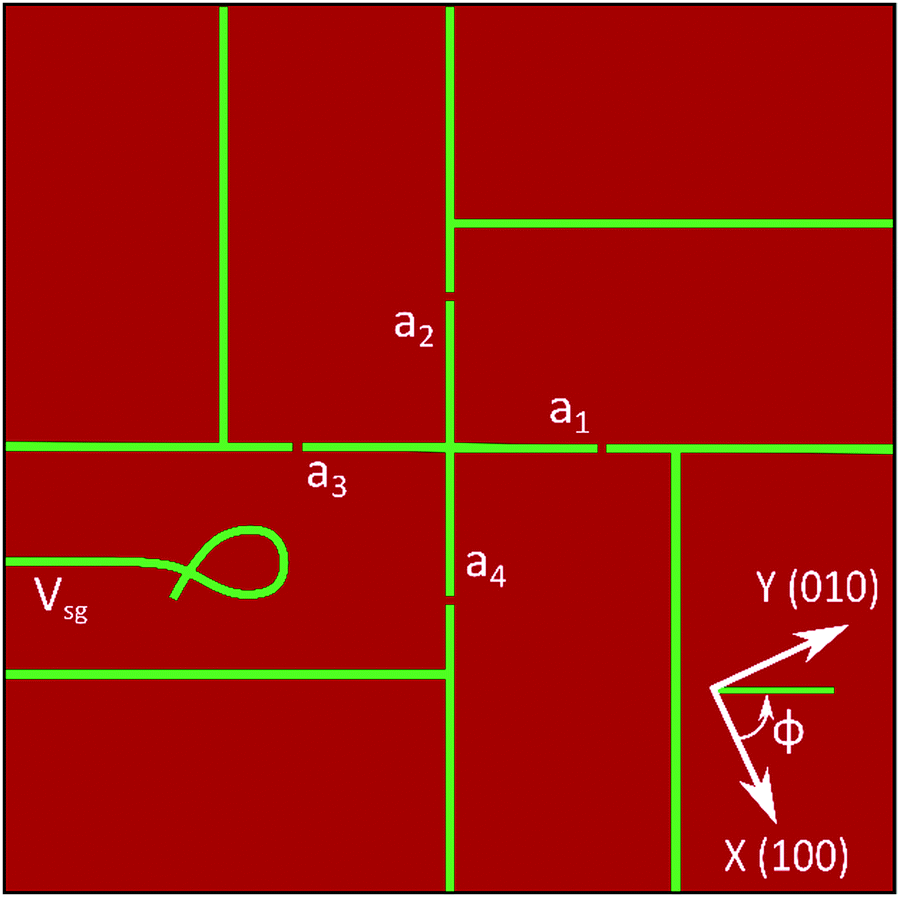 | ||
| Fig. 1 Schematic of LaAlO3/SrTiO3 nanocross written using c-AFM lithography. Four barriers of width ∼30 nm surround the main channels of length ∼1000 nm forming a nanocross which can be tuned by a proximal sidegate Vsg. Angle ϕ denotes the relative position of the nanocross with respect to the crystallographic direction. | ||
The six distinct current paths for the nanocross are illustrated in Fig. 2(a–f). There are two straight paths, namely, the horizontal (H) and vertical (V) configurations, and four “L shaped” paths (L1, L2, L3, L4). For each of these configurations, current I is sourced between the source (I+) and drain (I−) while voltages (V+/V−) are measured to produce four-terminal longitudinal conductance measurements as a function of applied gate voltages Vsg and external magnetic field B (see Fig. 2(a–f)).
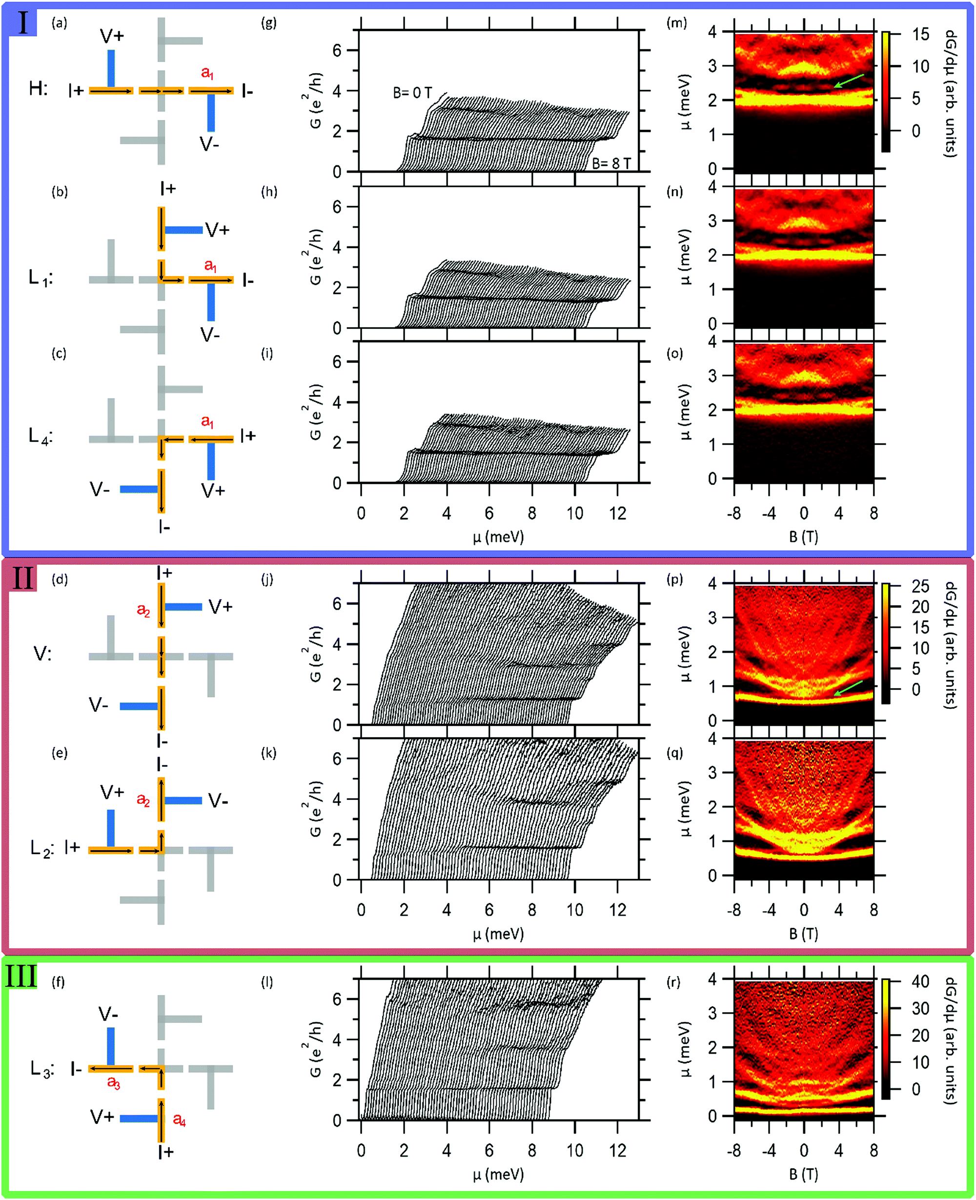 | ||
| Fig. 2 Longitudinal magnetoconductance measurements for the six configurations of the nanocross of Device A at ϕ = 65°, grouped on the basis of similar transconductance spectra. (a and d) Straight paths of the nanocross, (b, c, e and f) L-shaped paths of the nanocross, (g–l) zero-bias longitudinal conductance, G, as a function of chemical potential μ and magnetic field B in the range 0–8 T for the six configurations respectively. Data is shifted along x axis for clarity, (m–r) transconductance spectra dG/dμ shown as a function of μ and B for the six configurations. The green arrows illustrate signatures of universal conductance fluctuations. | ||
Results and discussion
The conductance of an electron waveguide primarily depends on the chemical potential μ and the applied magnetic field B. The chemical potential of the device can be tuned with the proximal side gate Vsg. For a quasi-1D straight electron waveguide11 written at the LAO/STO interface, the conductance is quantized near integer values of e2/h in the presence of an external magnetic field. The transport properties of LAO/STO heterostructures in 1D regime is intrinsically different from semiconductors systems like GaAs/AlGaAs. When patterned into 1D channels, repulsive interactions at semiconductor interfaces generally leads to a significant drop in mobility due to enhanced impurity or interface scattering.30–32 However, unlike semiconductor systems, attractive electron–electron interactions in LAO/STO heterostructures are believed to strongly suppress the scattering mechanism.11 The zero bias longitudinal conductance G = dI/dV for the six configurations of the nanocross of Device A is recorded as a function of the chemical potential μ for a sequence of magnetic fields between B = 0 and B = 8 T (Fig. 2(g–l)). Quantized conduction steps are observed in each of the six configurations, indicating the existence of ballistic transport. Transport in the nanocross remains ballistic till the lowest magnetic fields. The fractional values of the conductance quantization steps are attributed to weak interference effects due to the multiterminal nature of the device. Conductance quantization steps at values between e2/h and 2e2/h are associated with a paired electron state.11,12 Pairing is generally observed up to a critical “pairing field”, Bp which can be anywhere in the range 1–10 T.To reveal more information about the electronic structure within the nanocross, we calculate the transconductance dG/dμ and plot it as an intensity map as a function of B and μ. Transconductance spectra of the six configurations for Device A are plotted in Fig. 2(m–r). A peak in the transconductance marks the chemical potential at which a new subband contributes to transport (the subband bottom). The subbands are further separated by regions where the conductance is quantized (dG/dμ → 0). Insight into the nature of electron transport of the nanocross comes from arranging the transconductance spectra for the six configurations in decreasing order of the lowest subband bottom (Fig. 2(m–r)). The following observations can be made:
1. The transconductance spectra can be sorted into three groups based on similarity (see Fig. 2) (labeled I, II, III in Fig. 2). The group with the highest gate voltage threshold for conduction has the largest number of members (three for group I in the given case) and vice versa.
2. Within each group, the configurations share a common source (I+) or drain (I−). For example, group I shares a common arm a1, group II shares a common arm a2. The last group III is not distinctly associated with either of the two remaining arms (a3, a4).
3. The pairing field (Bp) differs among the three groups of the nanocross. Bp is lowest for group I ∼3 T, followed by group II and III (the pairing field exceeds 8 T).
4. The specific pattern of subband minima is highly reproducible from one c-AFM writing to the next, provided the nanocross is written in the same position and orientation on the LAO/STO sample (Fig. S2 and S3, ESI†).
5. Changing the orientation of the nanocross otherwise at the same position on the canvas, changes the nature of the transconductance spectra of each group (Fig. 3). However, the transconductance spectra of the rotated nanocross can still be identically sorted into groups I, II and III like that of Device A.
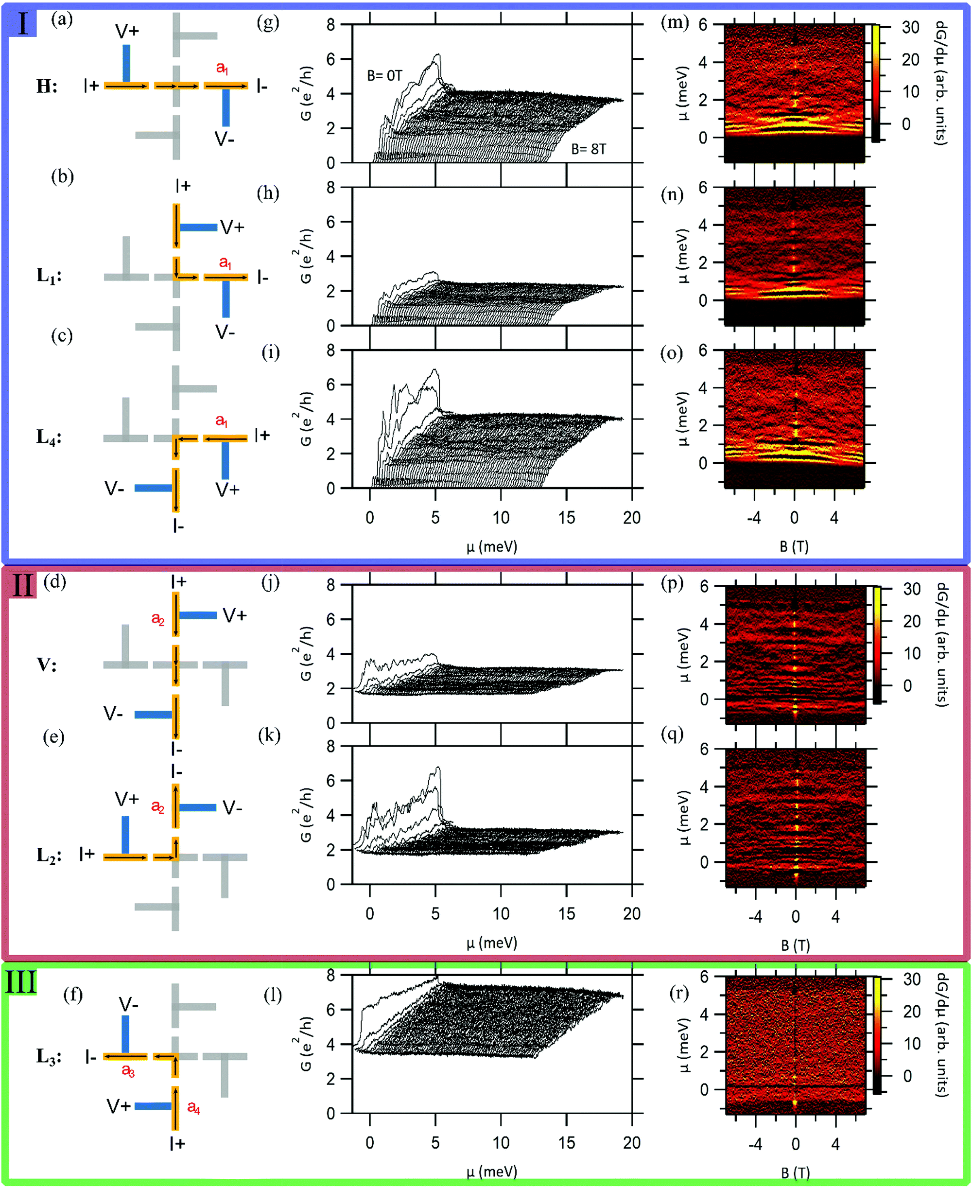 | ||
| Fig. 3 Longitudinal magnetoconductance measurements for the six configurations of the nanocross of Device D, at ϕ = 0°, grouped on the basis of similar transconductance spectra. (a and d) Straight paths of the nanocross, (b, c, e and f) L-shaped paths of the nanocross, (g–l) zero-bias longitudinal conductance, G, as a function of chemical potential μ and magnetic field B in the range 0–8 T for the six configurations respectively. Data is shifted along x axis for clarity, (m–r) transconductance spectra dG/dμ shown as a function of μ and B for the six configurations. | ||
6. We also observe some additional features (marked by green arrows) in the transconductance spectra of the six configurations of the nanocross (see Fig. 2). These features are not present in the transconductance spectra of most quasi-1D straight electron waveguides and are symmetric as a function of the magnetic field.
To get a finer picture of the transport properties across the nanocross, we plot the conductance of the vertical configuration (Gv) as an intensity map as a function of B and μ (Fig. 4(a)). Plots of conductance (Gv) versus magnetic field (B) are shown for selected values of chemical potential μ (Fig. 4(b)). Magnetic depopulation signatures are clearly observed, similar to those previously reported in straight electron waveguides.20 Superimposed on the magnetic depopulation signatures are prominent quasi-oscillatory features (marked by black lines in Fig. 4(b)), which are reproducible at a specific chemical potential but vary from one device to the next and change with magnetic field. The quasi-oscillatory features are identified as manifestations of universal conductance fluctuations (UCF).33–35 UCF also accounts for the additional features (mentioned in the observations above) in the transconductance spectra of the nanocross. Quantum interference effects like UCF have been previously reported in mesoscopic LAO/STO devices created by other techniques.35
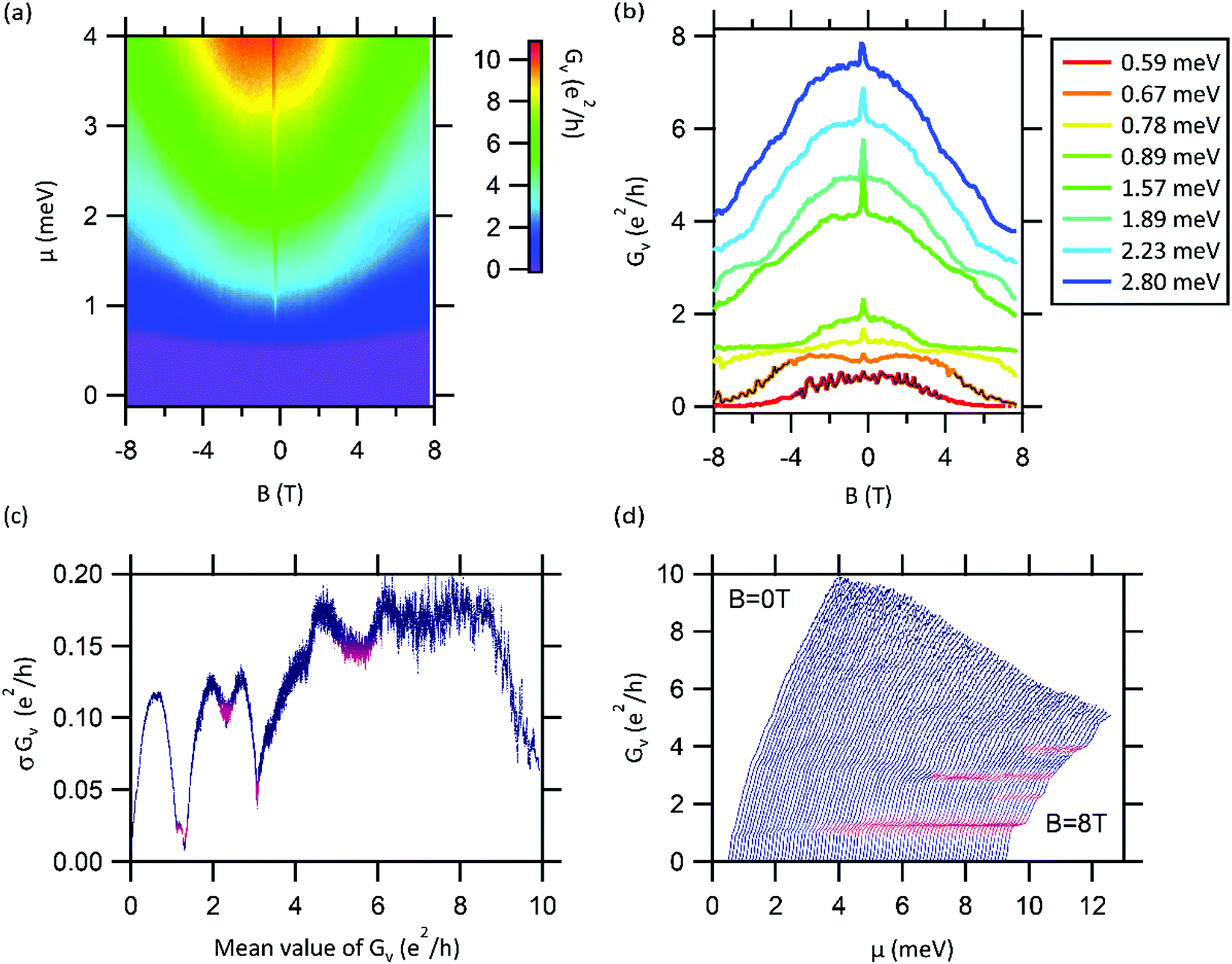 | ||
| Fig. 4 Conductance (Gv) of the vertical configuration (V) and signatures of universal conductance fluctuations (UCF) for the vertical (V) configuration. (a) Gv intensity plot as a function of chemical potential μ and magnetic field B, (b) line cuts of Gv intensity plot as a function of B at selected values of μ. Black lines highlight the quasi-oscillatory features of UCF, (c) standard deviation of Gv (σGv) as a function of the mean value of Gv, (d) Gv as a function of the chemical potential μ with B = 0 T to 8 T. Dips in (c) corresponds to plateaus in (d) (shaded pink). Data is shifted along x axis for clarity. | ||
Notably, the quasi-oscillatory features are particularly magnified for certain values of Gv (denoted by black lines in Fig. 4(b)) independent of the value of chemical potential and magnetic field (B < 4 T for μ = 0.59 meV and B > 4 T for μ = 0.67 meV). In order to understand this relationship, the standard deviation of Gv (σGv) is plotted versus the mean value of Gv (Fig. 4(c)). The procedure for obtaining the standard deviation and mean value of Gv is described in the ESI† (Fig. S4). Dips in the standard deviation (shaded pink) are clearly correlated with stable quantized values in the Gvversus μ plot (shaded pink in Fig. 4(d)), especially at low overall conductance values. Similar dips in conductance fluctuation (σGv) have been previously attributed to saturation of channel transmission in ballistic point contacts.36,37 The magnification of quasi-oscillatory features near the subband minima can be understood from a simple picture where the subband bottom of the nanowire acts like a “beam splitter” in the nanocross giving rise to magnified quantum interference effects. Similar phenomena have also been observed in mesoscopic LAO/STO devices.38
Magnetotransport measurements across the nanocross shows that there is significant inhomogeneity in the transport properties at the interface. In spite of extending 1 μm along two dimensions, the electronic band structure of the four arms of the nanocross exhibits pronounced inhomogeneity. To understand how inhomogeneities may arise in the nominally symmetric nanocross, we consider a simplified model (Fig. 5(a)) of how ferroelastic domains are expected to align with a nanocross device that is oriented along major crystallographic directions. The ferroelastic domains in STO can be oriented along the X (100), Y (010) or Z (001) crystalline direction, separated by nanometer-scale domain walls, with domain boundaries aligned according to the domain tiling rules (Fig. S5, ESI†).19 Specifically, near the surface of STO, the boundary between Z and X domains should lie at 0°, between Z and Y domains at 90° and between X and Y domains at 45° or 135°. While the lowest energy configuration is expected to have similar domain configuration across the four arms of the nanocross (Fig. 5(a)), far off boundary conditions may lead to an expansion or contraction of the X and Y domains, which can be parameterized by the angles δi, i = 1,…,4 (Fig. 5(b)). Movement of the X and Y domains is expected to produce a strain within the conductive nanowires. This in turn will affect the electronic band structure of the nanowire, shifting energy subbands up or down, accordingly. Thus, each arm of the nanocross is expected to have a unique electronic band structure, represented by its corresponding transconductance spectra. The measured conduction band energy difference (∼1 meV) between Z domain regions compared with X or Y domains19 is generally in good agreement with theoretical calculations,39 setting the overall scale of the energetics due to structural distortions of this type. Further, we consider the effect of rotation of the nanocross on the ferroelastic domain configuration across it. Fig. 5(c) shows a possible ferroelastic domain configuration for a nanocross rotated by an angle of 65° with respect to the (100) crystallographic direction, taking into account known tiling rules. The contiguous size and shape of the X and Y domains is expected to be altered by the rotation of the nanocross, although the domain configuration across each arm should remain identical in the lowest energy configuration. Additionally, as previously mentioned, expansion or contraction of the X and Y domains from the lowest energy configuration (parameterized by the angles δi′, i = 1,…,4 in Fig. 5(d)) can similarly lead to inhomogeneities across the four arms of the rotated nanocross.
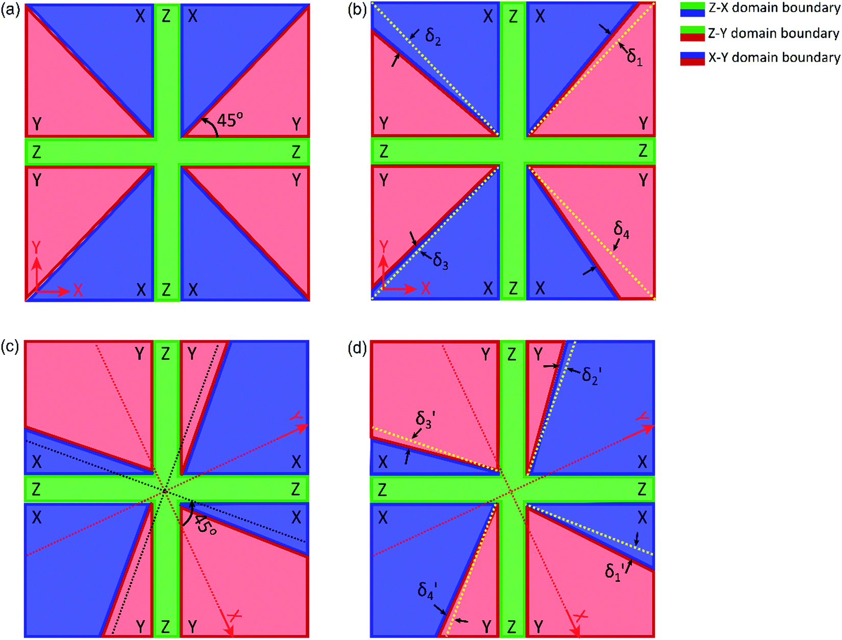 | ||
| Fig. 5 Ferroelastic domain configuration for the two orientations of the nanocross: (a) the domain configuration of a symmetric nanocross in the lowest energy configuration when oriented along the crystallographic direction (Device D), (b) expansion or contraction of the X and Y domains due to the presence of far-off boundary conditions producing a strain across the nanocross. For the given case δ1, δ2 > 0 and δ3, δ4 < 0. (c) The domain configuration of a symmetric nanocross in the lowest energy configuration when rotated by ϕ = 65° (Device A, B, C), (d) expansion or contraction of the X and Y domains due to the presence of far-off boundary conditions producing a strain across the nanocross. For the given case δ2′, δ3′ > 0 and δ1′, δ4′ < 0. The Z–X, Z–Y and X–Y domain boundaries have been defined by darker shades along the edges of the nanocross for all cases. | ||
We recall that all the configurations within a given group share a common current-carrying lead (I+ or I−) (Fig. 2). We consider this common arm to be the least conducting lead of the group, namely arm a1 for group I, arm a2 for group II and arm a3 or a4 for group III (Fig. 2). The least conducting lead dominates the conductance of a given configuration. Furthermore, electronic states within the nanocross are extended and delocalized. Together, these two assumptions help to account for observed similarities in transconductance spectra observed among all configurations within a group. Additionally, since the bottom of the first subband is at the highest value of μ for group I, followed by groups II and III respectively, arm a1 possibly represents the least conducting lead of the nanocross whereas arm a3 or a4 represents the most conducting leads.
Finally, we extend the ferroelastic domain model to understand the nature of electron pairing across the nanocross. The pairing field, Bp, is found to vary among the three groups of the transconductance spectra. We have reported similar variations in the value of Bp from one c-AFM writing to next in straight electron waveguides and SETs.11,12 However, due to limitations of the device geometry, these variations were not measured across a single device at a given chemical potential and magnetic field till date. In reports by Pai et al.,13 it has been suggested that the pairing mechanism at the LAO/STO interface is mediated by the ferroelastic domain boundaries. As previously mentioned, with c-AFM lithography we define the Z–X and Z–Y domain boundaries along the edges of the nanocross. Further, with the given domain model, we discussed the possibility of the X and Y domains deviating from their lowest energy configuration, producing an unequal strain across the nanocross arms. The resulting strain can shift the energy difference between the Z–X and Z–Y domains, differing along the four arms of the nanocross. Hence, these inhomogeneities can potentially account for the observed differences in the pairing field, Bp, across the four arms of the nanocross.
The experimental results reported here support the idea that the nanocross geometry, by its two-dimensional nature, constrains ferroelastic domains in the vicinity of the cross, thereby stabilizing the transport properties. Devices created at the same spatial position on the sample (and orientation) are highly reproducible in their magnetotransport properties from one c-AFM writing to the next. When grouped on the basis of decreasing threshold for conductance, the transport characteristics exhibit very similar transconductance spectra for all three devices. It was further shown that rotating the angle of the nanocross by ϕ with respect to crystallographic axis (without changing its location) significantly alters the transport properties of the nanocross. Future studies, possibly coupled with theoretical modeling (e.g., phase-field simulations40,41), may help to establish a more microscopic understanding of the interrelationships between electronic band structure, nanostructure geometry, and ferroelastic domain structure for LaAlO3/SrTiO3 nanostructures created by c-AFM lithography.
Conflicts of interest
There are no conflicts to declare.Acknowledgements
We acknowledge useful discussions with Yun-Yi Pai. This work is supported by Vannevar Bush Faculty Fellowship ONR grant N00014-15-1-2847 (J. L.). The work at University of Wisconsin-Madison was supported by the National Science Foundation (DMR-1629270) and the Air Force Office of Scientific Research (FA9550-15-1-0334).References
- Y.-Y. Pai, A. Tylan-Tyler, P. Irvin and J. Levy, Rep. Prog. Phys., 2018, 81, 036503 CrossRef PubMed
.
- J. A. Sulpizio, S. Ilani, P. Irvin and J. Levy, Annu. Rev. Mater. Res., 2014, 44, 117 CrossRef CAS
- A. Ohtomo and H. Y. Hwang, Nature, 2004, 427, 423–426 CrossRef CAS PubMed
- N. Reyren, S. Thiel, A. D. Caviglia, L. F. Kourkoutis, G. Hammerl, C. Richter, C. W. Schneider, T. Kopp, A. S. Ruetschi, D. Jaccard, M. Gabay, D. A. Muller, J. M. Triscone and J. Mannhart, Science, 2007, 317, 1196–1199 CrossRef CAS PubMed
- A. D. Caviglia, S. Gariglio, N. Reyren, D. Jaccard, T. Schneider, M. Gabay, S. Thiel, G. Hammerl, J. Mannhart and J. M. Triscone, Nature, 2008, 456, 624–627 CrossRef CAS PubMed
- A. Brinkman, M. Huijben, M. Van Zalk, J. Huijben, U. Zeitler, J. C. Maan, W. G. Van der Wiel, G. Rijnders, D. H. A. Blank and H. Hilgenkamp, Nat. Mater., 2007, 6, 493–496 CrossRef CAS PubMed
- G. Cheng, M. Tomczyk, A. B. Tacla, H. Lee, S. Lu, J. P. Veazey, M. Huang, P. Irvin, S. Ryu, C.-B. Eom, A. Daley, D. Pekker and J. Levy, Phys. Rev. X, 2016, 6, 041042 Search PubMed
- A. D. Caviglia, M. Gabay, S. Gariglio, N. Reyren, C. Cancellieri and J. M. Triscone, Phys. Rev. Lett., 2010, 104, 126803 CrossRef CAS PubMed
- M. Ben Shalom, M. Sachs, D. Rakhmilevitch, A. Palevski and Y. Dagan, Phys. Rev. Lett., 2010, 104, 126802 CrossRef CAS PubMed
- C. Cen, S. Thiel, J. Mannhart and J. Levy, Science, 2009, 323, 1026–1030 CrossRef CAS PubMed
- A. Annadi, G. Cheng, H. Lee, J.-W. Lee, S. Lu, A. Tylan-Tyler, M. Briggeman, M. Tomczyk, M. Huang, D. Pekker, C.-B. Eom, P. Irvin and J. Levy, Nano Lett., 2018, 18, 4473–4481 CrossRef CAS PubMed
- G. Cheng, M. Tomczyk, S. Lu, J. P. Veazey, M. Huang, P. Irvin, S. Ryu, H. Lee, C. B. Eom, C. S. Hellberg and J. Levy, Nature, 2015, 521, 196 CrossRef CAS PubMed
- Y.-Y. Pai, H. Lee, J.-W. Lee, A. Annadi, G. Cheng, S. Lu, M. Tomczyk, M. Huang, C.-B. Eom, P. Irvin and J. Levy, Phys. Rev. Lett., 2018, 120, 147001 CrossRef CAS PubMed
- Y. Frenkel, N. Haham, Y. Shperber, C. Bell, Y. Xie, Z. Chen, Y. Hikita, H. Y. Hwang and B. Kalisky, ACS Appl. Mater. Interfaces, 2016, 8, 12514–12519 CrossRef CAS PubMed
- N. J. Goble, R. Akrobetu, H. Zaid, S. Sucharitakul, M.-H. Berger, A. Sehirlioglu and X. P. A. Gao, Sci. Rep., 2017, 7, 44361 CrossRef PubMed
- R. A. Cowley, Phys. Rev., 1964, 134, A981–A997 CrossRef
- Y. Frenkel, N. Haham, Y. Shperber, C. Bell, Y. Xie, Z. Chen, Y. Hikita, H. Y. Hwang, E. K. H. Salje and B. Kalisky, Nat. Mater., 2017, 16, 1203–1208 CrossRef CAS PubMed
- B. Kalisky, E. M. Spanton, H. Noad, J. R. Kirtley, K. C. Nowack, C. Bell, H. K. Sato, M. Hosoda, Y. Xie, Y. Hikita, C. Woltmann, G. Pfanzelt, R. Jany, C. Richter, H. Y. Hwang, J. Mannhart and K. A. Moler, Nat. Mater., 2013, 12, 1091–1095 CrossRef CAS PubMed
- M. Honig, J. A. Sulpizio, J. Drori, A. Joshua, E. Zeldov and S. Ilani, Nat. Mater., 2013, 12, 1112–1118 CrossRef CAS PubMed
- G. Cheng, A. Annadi, S. Lu, H. Lee, J.-W. Lee, M. Huang, C.-B. Eom, P. Irvin and J. Levy, Phys. Rev. Lett., 2018, 120, 076801 CrossRef CAS PubMed
- H. Noad, E. M. Spanton, K. C. Nowack, H. Inoue, M. Kim, T. A. Merz, C. Bell, Y. Hikita, R. Xu, W. Liu, A. Vailionis, H. Y. Hwang and K. A. Moler, Phys. Rev. B, 2016, 94, 174516 CrossRef
- M. Ben Shalom, C. W. Tai, Y. Lereah, M. Sachs, E. Levy, D. Rakhmilevitch, A. Palevski and Y. Dagan, Phys. Rev. B: Condens. Matter Mater. Phys., 2009, 80, 140403 CrossRef
- A. Annadi, Z. Huang, K. Gopinadhan, X. R. Wang, A. Srivastava, Z. Q. Liu, H. H. Ma, T. P. Sarkar, T. Venkatesan and Ariando, Phys. Rev. B: Condens. Matter Mater. Phys., 2013, 87, 201102 CrossRef
- S. Seri and L. Klein, Phys. Rev. B: Condens. Matter Mater. Phys., 2009, 80, 180410 CrossRef
- H.-L. Hu, R. Zeng, A. Pham, T. T. Tan, Z. Chen, C. Kong, D. Wang and S. Li, ACS Appl. Mater. Interfaces, 2016, 13630–13636, DOI:10.1021/acsami.6b01518
- C. Cen, S. Thiel, G. Hammerl, C. W. Schneider, K. E. Andersen, C. S. Hellberg, J. Mannhart and J. Levy, Nat. Mater., 2008, 7, 298–302 CrossRef CAS PubMed
- M. Huang, F. Bi, S. Ryu, C.-B. Eom, P. Irvin and J. Levy, APL Mater., 2013, 1, 052110 CrossRef
- G. Cheng, P. F. Siles, F. Bi, C. Cen, D. F. Bogorin, C. W. Bark, C. M. Folkman, J. W. Park, C. B. Eom, G. Medeiros-Ribeiro and J. Levy, Nat. Nanotechnol., 2011, 6, 343–347 CrossRef CAS PubMed
- F. Bi, D. F. Bogorin, C. Cen, C. W. Bark, J. W. Park, C. B. Eom and J. Levy, Appl. Phys. Lett., 2010, 97, 173110 CrossRef
- G. Timp, A. M. Chang, P. Mankiewich, R. Behringer, J. E. Cunningham, T. Y. Chang and R. E. Howard, Phys. Rev. Lett., 1987, 59, 732–735 CrossRef CAS PubMed
- T. Giamarchi and H. J. Schulz, Phys. Rev. B: Condens. Matter Mater. Phys., 1988, 37, 325–340 CrossRef
- C. L. Kane and M. P. A. Fisher, Phys. Rev. B: Condens. Matter Mater. Phys., 1992, 46, 15233–15262 CrossRef
- A. D. Stone, Phys. Rev. Lett., 1985, 54, 2692–2695 CrossRef CAS PubMed
- P. A. Lee and A. D. Stone, Phys. Rev. Lett., 1985, 55, 1622–1625 CrossRef CAS PubMed
- D. Rakhmilevitch, M. Ben Shalom, M. Eshkol, A. Tsukernik, A. Palevski and Y. Dagan, Phys. Rev. B: Condens. Matter Mater. Phys., 2010, 82, 235119 CrossRef
- B. Ludoph, M. H. Devoret, D. Esteve, C. Urbina and J. M. van Ruitenbeek, Phys. Rev. Lett., 1999, 82, 1530–1533 CrossRef CAS
- D. L. Maslov, C. Barnes and G. Kirczenow, Phys. Rev. B: Condens. Matter Mater. Phys., 1993, 48, 2543–2552 CrossRef CAS
- P. Irvin, H. Lee, M. Briggeman, S. Liu, A. Annadi, G. Cheng, M. Tomczyk, M. Huang, C.-B. Eom and J. Levy, 2017, in preparation.
- E. Heifets, E. Kotomin and V. A. Trepakov, J. Phys.: Condens. Matter, 2006, 18, 4845 CrossRef CAS
- F. Xue, Y. Li, Y. Gu, J. Zhang and L.-Q. Chen, Phys. Rev. B: Condens. Matter Mater. Phys., 2016, 94, 220101 CrossRef
- J.-J. Wang, B. Wang and L.-Q. Chen, Annu. Rev. Mater. Res., 2019, 49 DOI:10.1146/annurev-matsci-070218-121843
Footnote |
| † Electronic supplementary information (ESI) available. See DOI: 10.1039/c9nh00188c |
| This journal is © The Royal Society of Chemistry 2019 |