
Dipole controlled Schottky barrier in the blue-phosphorene-phase of GeSe based van der Waals heterostructures†
Lei
Peng
a,
Yu
Cui
a,
Liping
Sun
a,
Jinyan
Du
 a,
Sufan
Wang
a,
Shengli
Zhang
*b and
Yucheng
Huang
*a
a,
Sufan
Wang
a,
Shengli
Zhang
*b and
Yucheng
Huang
*a
aCollege of Chemistry and Material Science, The Key Laboratory of Functional Molecular Solids, Ministry of Education, Anhui Laboratory of Molecule-Based Materials, Anhui Normal University, Wuhu 241000, China. E-mail: huangyc@mail.ahnu.edu.cn
bKey Laboratory of Advanced Display Materials and Devices, Ministry of Industry and Information Technology, College of Material Science and Engineering, Nanjing University of Science and Technology, Nanjing 210094, China. E-mail: zhangslvip@njust.edu.cn
First published on 16th November 2018
Abstract
Controlling the interface structure is of utmost importance to regulating the nanoscale Schottky barrier height (SBH). Herein, by using first-principles calculations, the electronic properties of the graphene (G) based blue-phosphorene-phase of GeSe van der Waals (vdW) heterostructures, including M/G and X/G interfaces (M = Ge; X = Se), are systematically investigated. When the layer spacing exceeds the vdW gap, n-type Schottky contacts are formed for both MX/G and XM/G heterojunctions. With the layer spacing decreasing to equilibrium distances, due to different charge transfer across the interface, MX/G and XM/G heterojunctions display n- and p-type Schottky contacts, respectively. Further decreasing the layer distance makes both heterojunctions transit into p-type ones. The layer-spacing-dependent SBHs can be rationalized by the increased charge transfer across the interface and the resulting interfacial dipole enhancement. Enlightened by the finding of dipole-controlled SBHs, using MX as building blocks, two different stacking patterns, i.e., nMX–MX–G and nXM–XM–G (n = 1 and 2), are designed to further modulate the SBH. Interestingly, due to the presence of the intrinsic dipole of MX, it is found that the magnitude and orientation of the interfacial dipole can be artificially engineered. With n increasing from 0 to 2, nMX–MX–G with an X/G interface changes from the n-type Schottky contact to Ohmic contact. The Fermi level meets the conduction band and G shows a p-type doping feature finally. Likewise, transition from p-type Schottky contact to Ohmic contact is observed for the nXM–XM–G with M/G interface, accompanied by the Fermi level touching the valence band and the feature of n-type doping for G. The role of nMX stacking seems like the role of applying an external electric field (E-field): applying positive E-field is equivalent to the increase of dipole moment while negative E-field corresponds to the offset of dipole moment. In brief, the SBHs of GeSe/G contact are found to be tunable which originates from the intrinsic dipole of MX. The predictable SBHs for these kinds of charming built-in dipole systems are expected to be highly desirable in electronic devices.
Conceptual insightsGraphene (G)-based semimetal–semiconductor contacts have been extensively studied owing to their tunable nanoscale Schottky barrier height (SBH) by means of applying an external electric field (E-field), altering the interlayer spacing, etc. Here, using first-principles calculations, dipole-controlled SBH in the G-based blue-phosphorene-phase of GeSe van der Waals (vdW) heterostructures is reported. As Ge and Se atoms distribute over two different sides of GeSe, two possible stacking modes, i.e., GeSe–G with Se/G interface and SeGe–G with Ge/G interface are constructed. Conventional means of altering the interlayered spacing can make both GeSe–G and SeGe–G Schottky contacts transition from n- to p-type. The increase of charge transfer and corresponding interfacial dipole are revealed to account for the reason of regulatable SBH. Inspired by the established physical picture between charge transfer, interfacial dipole and potential step, using GeSe as building blocks, nGeSe–GeSe–G and nSeGe–SeGe–G (n = 1 and 2) stackings are designed to further regulate the SBHs. Interestingly, the role of GeSe stacking seems like the role of applying E-field: applying positive E-field is equivalent to the increase of dipole moment while negative E-field corresponds to the offset of dipole moment. The concept of dipole-controlled SBH is of utmost significance to guiding the design of new generation G-based contacts. |
Introduction
Owing to the remarkable properties such as high carrier mobility, intriguing quantum Hall effect, exceptional mechanical strength and massless Dirac fermion, graphene,1 one of the typical representatives in the two-dimensional (2D) material family, has attracted considerable interest over the past decade. Although it is an extremely promising material as a building block for the design of future nanoelectronic devices,1–3 the absence of a band gap and fast carrier recombination limit its optoelectronic applications. Combining graphene with other 2D materials by forming heterojunctions is one of the strategies to expand the scope of its application. Actually, various 2D ultrathin G-based vdW heterostructures have been widely studied both experimentally and theoretically, such as G/MoS2,4–11 G/h-BN,12–16 G/GaSe,17–21 G/MoSSe,22,23 G/phosphorene24–27 and G/blue phosphorene.28,29 For example, G/MoS2 has been synthesized for use in memory devices and electronic devices, with the on/off current ratio being tuned to be as high as ∼100.5,11 G/h-BN based devices were proved to be highly promising for efficient and stable electrical-to-optical signal conversion in photonic interconnects.12 Moreover, it was revealed that hybrid composites of G/phosphorene are promising candidates for future energy storage devices.26 By using G as the contact in a device rather than the channel, it was demonstrated that the Schottky barrier height (SBH) in G/phosphorene can be effectively tuned via the application of a perpendicular electric field.25 These vdW heterostructures show many novel properties far beyond their separate counterparts, which greatly extends their potential applications in many fields.30Generally, G-based vdW heterostructures with a typical semimetal–semiconductor contact can form a Schottky or Ohmic contact at the interface. Based on the Schottky–Mott model,31 n-type SBH ΦBn is defined as the energy difference between the Fermi level EF and conduction band minimum EC (ΦBn = EC − EF), while p-type SBH ΦBp is measured by the energy difference between the valence band maximum EV and the EF (ΦBp = EF − EV). When SBH becomes negative, an Ohmic contact is formed. The tunable SBH is an additional degree of freedom which is crucial for efficient operation of the device.32 Previous studies have shown that SBH of G-based vdW heterostructures can be effectively tuned by altering the layer spacing and applying a perpendicular electric field (E-field).17,25,27–29,33 Very recently, Si et al. found that the interface dipole, which depends on the electronegativity difference between C and the atom that is in contact with G, plays a key role in the regulation of SBH.20 Therefore, it can be anticipated that if a semiconductor with an intrinsic dipole contacts with G, the SBH would be artificially regulated by stacking in different patterns, in which the interface dipole moments can be controlled to be enhanced/weakened in different directions.
Recently, as phosphorene analogues,34–36 2D group IV monochalcogenides (MX, M = Ge, Sn; X = Se, S) have been predicted to have both black-phosphorene-phase37 and blue-phosphorene-phase.38 The structures of blue-phosphorene-phase group IV monochalcogenides can be viewed as the M and X atoms respectively substitute the neighboring P of the blue phosphorene, generating an intrinsic dipole with the direction from M- to X-side. Accordingly, the tunable SBH is expected to be achieved for heterostructures formed by G and such blue-phosphorene-phase group IV monochalcogenides.
In this work, by using first-principles calculations, the electronic structures and interface properties of GeSe/G heterostructures are systematically studied. The results show that an n-/p-type Schottky contact is formed when the M-/X-side contacts with G. SBHs can be regulated through altering interlayer distance. The underlying reason is revealed as the charge transfer and the corresponding interfacial dipole increase with the interlayer distance decreasing. Using MX as building blocks, nMX–MX–G and nXM–XM–G (n = 1 and 2) stackings are designed to further regulate the SBHs. With n increasing, nMX–MX–G and nXM–XM–G heterojunctions change from n-type and p-type Schottky contact to Ohmic contact, respectively. Interestingly, stacking multilayered GeSe with G leads to the same consequence as the E-field. Thus, through altering interlayer distance, stacking in different patterns and applying electric field, the interfacial dipoles of the GeSe/G system can be artificially modified which results in the predictable regulation of SBH.
Computational methods
First-principles calculations were performed using the projector augmented wave method39 in the Perdew–Burke–Ernzerhof (PBE) form of the generalized gradient approximation (GGA) for exchange and correlation40,41 as implemented in the Vienna ab initio simulation package (VASP).42 The DFT-D2 dispersion correction method was used to correctly describe the effect of the vdW interaction.43 The cutoff energy was set to be 400 eV for the plane wave expansion. The convergence thresholds were set to 10−5 eV and 0.01 eV Å for energy and force, respectively. Integrations over the first Brillouin-zone were performed using a 9 × 9 × 1 Monkhorst–Pack k-point grid. A vacuum height of 20 Å was used to avoid the interaction between two adjacent images. The dipole correction along the vertical direction was employed to accelerate the electronic convergence. Moreover, the hybrid functional of Heyd–Scuseria–Ernzerhof (HSE06)44 was used on some occasions to obtain more accurate electronic band structures. The spin–orbital coupling (SOC) tests were carried out to verify its effects on the electronic properties of the heterostructures.Results and discussion
We first investigated the structural parameters and electronic properties of G and 2D blue-phosphorene-phase GeSe. The lattice constants of G and GeSe monolayers are optimized to be 2.46 and 3.66 Å, respectively, in good agreement with previous studies (Tables 1 and 2).27,45 Considering the lattice mismatch between G and GeSe in the construction of a heterostructure, a 3 × 3 supercell of G and a 2 × 2 supercell of GeSe is stacked normal to the surface as shown in Fig. 1a–d, resulting in negligible lattice mismatch of around 0.73%. Different from the common non-polarized 2D materials, blue-phosphorene-phase GeSe has an intrinsic dipole pointing from Ge to Se. Thus, both the M- and X-side can approach G when it forms the heterostructures, giving rise to two different stacking modes, i.e., MX–G with X/G interface and XM–G with M/G interface. After interlayer distance scanning, the equilibrium distances at 3.42 and 3.41 Å are the most stable in energy for the MX–G and XM–G, respectively (Fig. 1e). The calculated interlayer distances are much larger than the sum of the covalent radii of interfacial atoms, indicating that vdW interactions are dominant in between the layers. In order to quantitatively characterize the stability of MX–G and XM–G, evolution of binding energies as a function of the interlayer distances is shown in Fig. 1e. The binding energy Eb is defined as | (1) |
| a (Å) | Work function (eV) | Φ Bn (eV) | Φ Bp (eV) | Dipole moment (Debye) | |
|---|---|---|---|---|---|
| Graphene | 2.46, (2.47),27 (2.46 ± 0.04)47 | 4.23, (4.24),27 (4.23)48 | N/A | N/A | 0 |
| MX–G | 7.39 | 4.27 | 0.76 (PBE) | 1.45 (PBE) | 0.30 |
| 0.99 (HSE06) | 1.92 (HSE06) | ||||
| 2MX–G | 7.38 | 4.29 | 0.07 | 0.87 | 0.98 |
| 3MX–G | 7.42 | 4.59 | ∼ 0 | 0.26 | 1.36 |
| XM–G | 7.39 | 4.30 | 1.50 (PBE) | 0.72 (PBE) | −1.27 |
| 1.75 (HSE06) | 1.02 (HSE06) | ||||
| 2XM–G | 7.39 | 4.06 | 0.95 | 0.03 | −1.74 |
| 3XM–G | 7.41 | 3.79 | 0.36 | ∼0 | −1.89 |
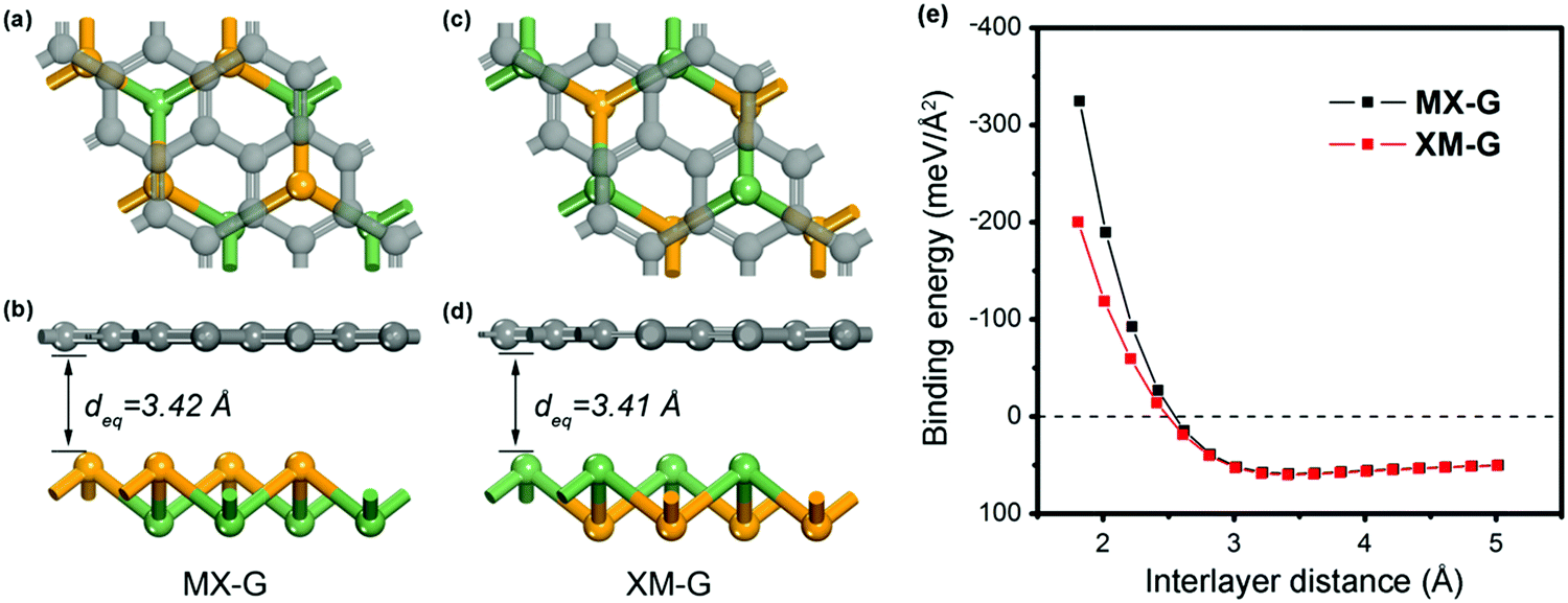 | ||
| Fig. 1 Top and side views of MX–G (a and b) and XM–G (c and d). (e) Binding energy of the heterostructures as a function of interlayer distance. | ||
Then, the electronic band structures of blue-phosphorene-phase GeSe, and pristine G as well as GeSe/G are investigated at different levels of theory (PBE and HSE06). As seen in Fig. 2a and b, GeSe has an indirect band gap of 2.25 eV (PBE) and 2.95 eV (HSE06), which is also consistent with previous results at the same calculation level.38,45 For G, the Dirac cone across the EF is well predicted at both the PBE and HSE06 levels. However, HSE06 gives a steeper energy dispersion around the Dirac cone than PBE. Thus, HSE06 would predict the larger Fermi velocity.49,50 Moreover, the Dirac cone is mapped to the Γ-point compared with the primitive cell of G which is due to the K and K′ points being folded to the Gamma point in the 3 × 3 G supercell.51
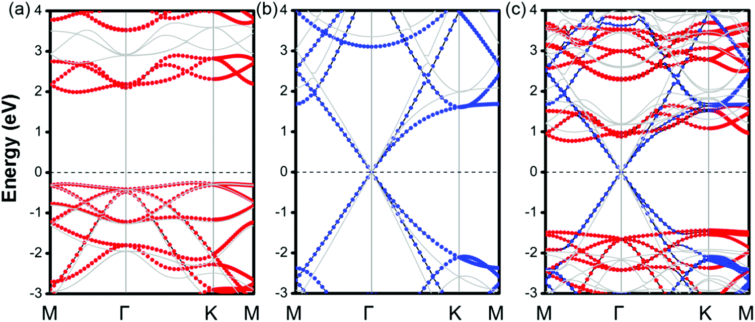 | ||
| Fig. 2 Electronic band structures of a blue-phosphorene-phase GeSe monolayer with a 2 × 2 supercell (a), G with a 3 × 3 supercell (b) and the MX–G heterostruture (c) at the PBE and HSE06 level. The electronic states contributed by GeSe and G are shown in red and blue dots at the PBE level, respectively. The light gray line represents the results of HSE06. | ||
The projected band structures of MX–G are shown in Fig. 2c. Here, blue and red symbols denote the contributions from the G and GeSe, respectively. Compared with the band structures of independent GeSe and G shown in Fig. 2a and b, the band structure of MX–G seems to be a simple superposition of each component. The Dirac cone of G remains intact at the EF. The morphology of the band energy dispersion and the value of the band gap of GeSe are also almost unchanged. These results are consistent with the typical features of a 2D vdW heterojunction, i.e., the key characteristics of independent components are maintained.
As is known, a Schottky contact would be formed if a semiconductor contacts with a metal. For the MX–G vdW heterojunction, it can form an n-type Schottky contact, which is similar to the G/blue-phosphorene system.29 As measured in Fig. 2c, ΦBn is 0.76 eV (PBE) or 0.99 eV (HSE06), which is much lower than ΦBp of 1.45 eV (PBE) or 1.92 eV (HSE06) (Table 1). Note that the ratio of ΦBn to ΦBp calculated by either PBE or HSE06 is almost the same. This scenario indicates that PBE functionals are available in predicting correct trends and physical mechanisms, although conventional DFT methods are generally known to underestimate the band gap of semiconductors and overestimate the charge transfer across the interface.52,53 Therefore, to avoid huge computational burden, the following results are mainly calculated at the PBE level. Meanwhile, the SOC effect on the electronic structure of MX–G was also carefully examined. As shown in Fig. S1 (ESI†), the SOC effects have insignificant change in the band dispersion of MX–G, thus, they are not taken into consideration in the following calculations.
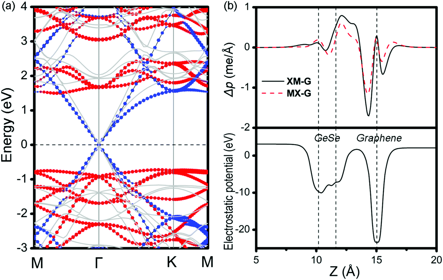
It is known that a tunable SBH is very important in electronic device applications.32 Generally, adjusting the interface distance is a viable means that can effectively control the SBH of G-based vdW heterostructures.29,54 We thus explored the effects of the interfacial spacing on the electronic structures of MX–G. The projected band structures with the selected distances (d = 2.62, 3.42 and 5.02 Å) are shown in Fig. 3a–c. The distance of 5.02 Å is deemed as the non-interacting system. It can be clearly seen that, as the interfacial distance decreases, the Dirac point of G moves towards the valence band (VB) of GeSe, resulting in a transition from the n-type Schottky contact to the p-type one. In Fig. 3d, we plot the SBHs as a function of the interlayer distance. As the interface distance decreases, ΦBn gradually increases while ΦBp gradually decreases, resulting in a crossover at a distance of 3.02 Å. Note that, ΦBn (ΦBp) finally converges to ∼ 0.42 eV (1.82 eV) when the interfacial distance exceeds that of vdW interaction.
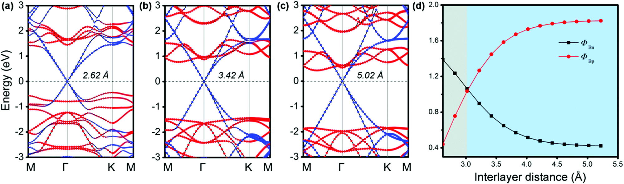 | ||
| Fig. 3 (a–c) Electronic band structures of MX–G with different interlayer distances. The red and blue symbols denote the contributions from GeSe and G, respectively. (d) The SBHs in MX–G as a function of the interlayer distance. | ||
To get insight into the transition from n- to p-type contact, plane-averaged differential charge densities (PDCD) and electrostatic potentials of MX–G varied with different interfacial distance along the vacuum direction are illustrated in Fig. 4a and b. PDCD is used here to illustrate the charge transfer between MX and G, which is defined as Δρ(z) = ρMX–G − ρGeSe − ρG, where ρMX–G is the plane-averaged charge density of MX–G, and ρGeSe and ρG are the individual plane-averaged charge densities of GeSe and G, respectively. As is seen from Fig. 4a, electrons are transferred from G to GeSe. With the distance decreasing, the amount of transferred electrons increases, and meanwhile, the potential well of G notably becomes deeper, leading to a stronger interfacial electrostatic field (Fig. 4b).
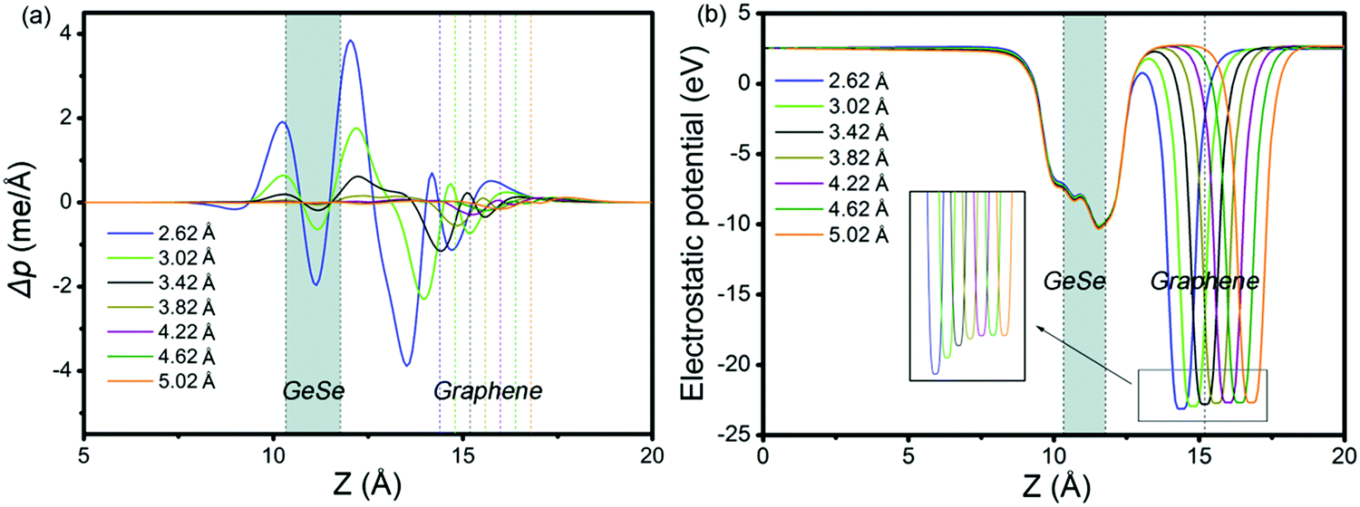 | ||
| Fig. 4 (a) Plane-averaged differential charge density and (b) electrostatic potentials of MX–G with different interlayer distances. | ||
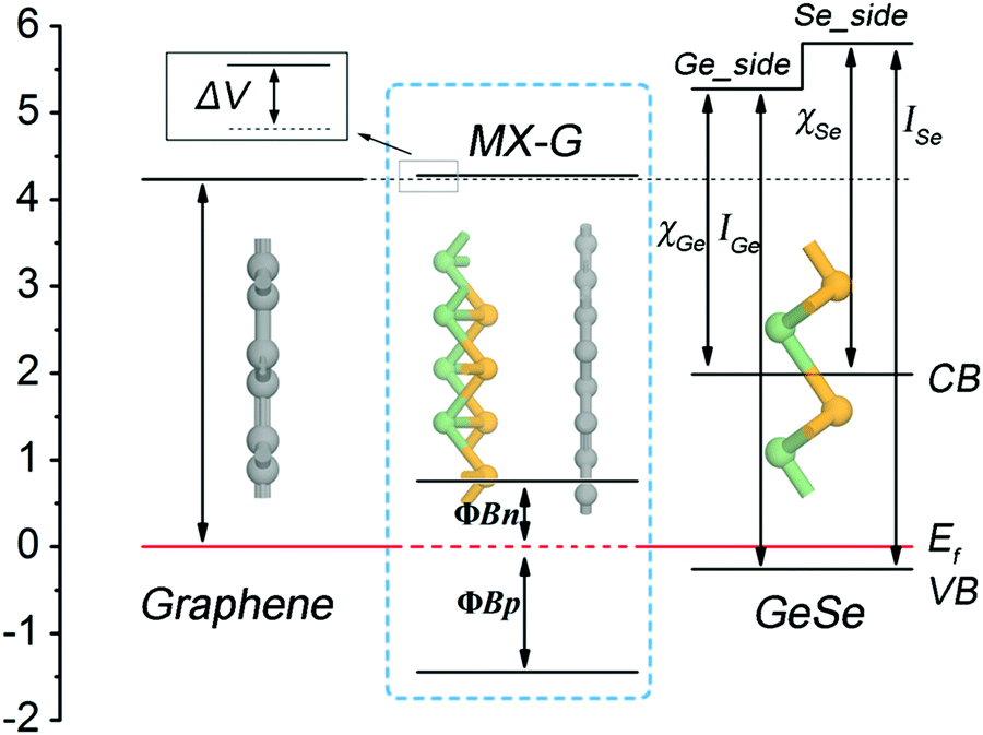
Interestingly, how the enhancement of charge transfer (CT) affects the SBH with the decrease of interlayer spacing can be well understood from the diagram presented in Fig. 5, in which an energy band diagram of isolated G, an isolated GeSe monolayer and the MX–G heterostructure aligned with the same EF are portrayed. Note that the Schottky contact of MX–G via vertical stacking is different from traditional metal–semiconductor Schottky ones via in-plane stitching.31 One major difference is that MX–G has weak vdW interactions without dangling bonds at the interface.27 Although such a vdW interaction is weak, it can create an interface dipole, accompanied by a potential step (ΔV) formed at the interface (Fig. 5).20 In these cases, the SBH under the Schottky–Mott rule considered ΔV should be rewritten as
| ΦBp = ISe − (WG + ΔVX) |
| ΦBn = (WG + ΔVX) − χSe | (2) |
 | ||
| Fig. 5 The energy band diagram of isolated G, MX and MX–G heterostructures. | ||
At the large enough interlayer distance, CT across the interlayer is ignorable, thus MX–G has the same work function as G. In this case, the ΦBn and ΦBp converge to WG − χSe and ISe − WG, respectively (formula (2)). As χSe, ISe and WG are calculated to be 3.81, 6.06 and 4.23 eV at the PBE level (Tables 1 and 2), respectively, the converged ΦBn (ΦBp) is 0.42 (1.83) eV, which is in nice agreement with the values measured from the band structure (Fig. 3c).
With the interlayer distance of MX–G decreasing, CT from G to MX increases, and simultaneously, ΔVX gradually increases as well (see below). This increase leads to the whole uplift of the positions of W, the conduction band (CB) and the VB of MX–G, thus, the EF, which is nearer to the CB at the beginning, begins to shift toward the VB, resulting in the transition of the Schottky contact from n- to p-type finally.
As analyzed above, the interlayered CT can effectively regulate the SBH of MX–G. Because GeSe has an intrinsic dipole, we flip it over and make the M-side contact with G. This would be very interesting, as the M/G interface may have different CT and may result in a different SBH modulation mechanism. From the electrostatic potential of MX–G (Fig. 4b), the potential difference between M and C is notably larger than that between X and C, which is consistent with the electronegativity order of 2.5 (C) > 2.4 (Se) > 2.0 (Ge). Thus, it can be predicted that the XM–G heterojunction would form a stronger electrostatic field and a larger interfacial dipole than that of MX–G. According to the formula (2), a resulting larger ΔVM of XM–G would lead to ΦBn/ΦBp increasing/decreasing. Actually, the calculated band structure of XM–G as shown in Fig. 6a is well consistent with our speculation. A p-type Schottky contact is formed at the M/G interface where ΦBp is measured to be 0.72 (1.02) eV and ΦBn is 1.50 (1.75) eV at the PBE (HSE06) level, respectively (Table 1). In Fig. 6b, we plot the PDCD and the electrostatic potential. Obviously, CT at the M/G interface is stronger than X/G, as expected. Due to considerable CT from C to Ge, the Dirac point of G opens slightly (18 and 28 meV under PBE and HSE06 level, respectively). However, this tiny gap is acceptable compared with thermal fluctuation (26 meV) at room temperature.
 | ||
| Fig. 6 (a) Electronic band structures of XM–G at the equilibrium distance. The red and blue symbols denote the contributions from GeSe and G, respectively. (b) Plane-averaged differential charge density and electrostatic potentials of XM–G. | ||
The change in interlayer distance also strongly affects its SBH for XM–G (Fig. S2, ESI†). For the non-interacting case, the n-type Schottky contact is formed and the value of SBH can be foreseen: ΦBn = WG − χGe = 4.23 − 3.29 = 0.94 eV, ΦBp = IGe − WG = 5.54 − 4.23 = 1.31 eV. When the interlayer distance decreases, CT from G to M enhances, therefore, according to the analysis from the results of MX–G, ΔVM would increase and the EF would shift towards VB, and the Schottky contact of XM–G is expected to change from n- to p-type, which is consistent with the observation shown in Fig. S2 (ESI†).
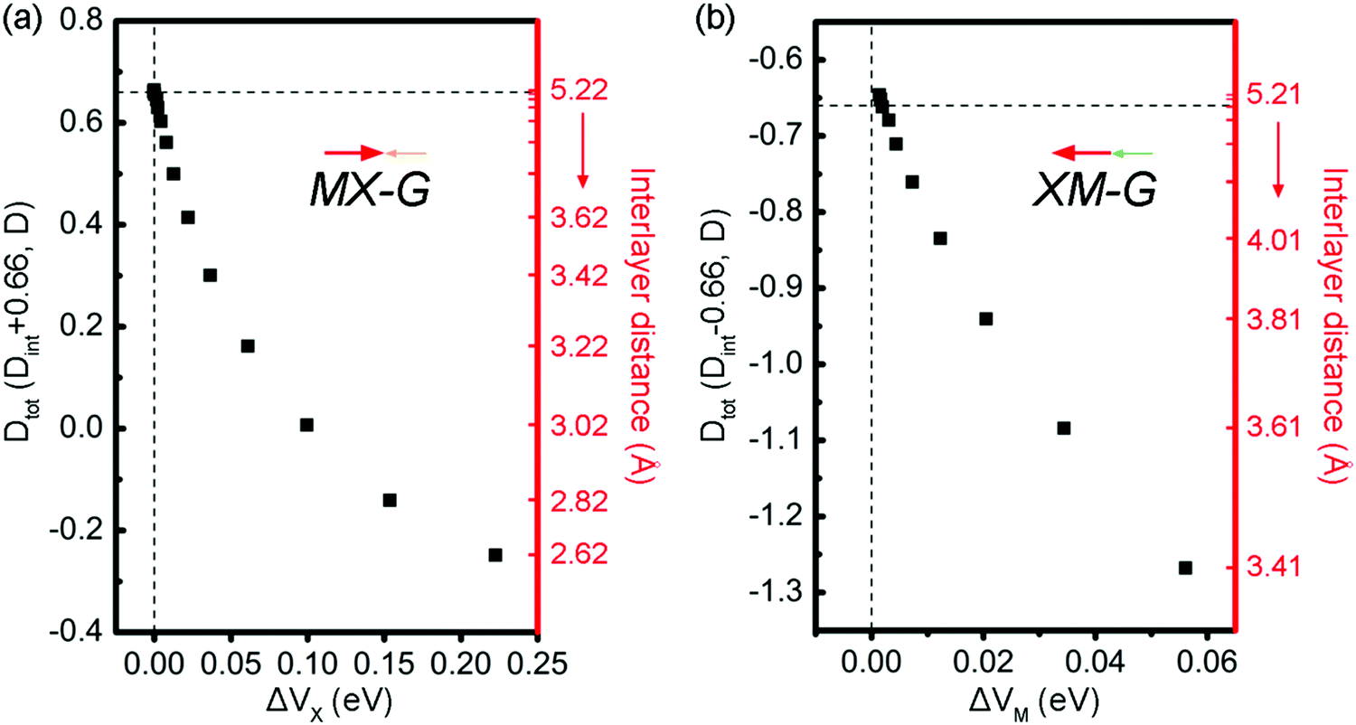
The intensity of CT across the interface determines the interface dipole (Dint). Due to the existence of an intrinsic dipole, Dint is defined as Dtot minus D0. Dtot and D0 are the dipole moments of the heterostructures and GeSe, respectively. Here, the positive direction is specified from GeSe to G. The calculated D0 is 0.66 D (Debye) for the isolated 2 × 2 GeSe supercell at the PBE level and the direction is from Ge to Se. When GeSe and G form the vdW heterojunctions, due to electrons transfer from G to MX, Dtot of MX–G is partially offset while that of XM–G is enhanced. At the equilibrium states, Dtot is calculated to be 0.3 and −1.27 D for the MX–G and XM–G, respectively (Table 1). The decreased magnitude of dipole moment for the MX–G is because the direction of the dipole generated at the interface is opposite to that of the GeSe itself, while the increased magnitude of dipole moment for the XM–G is due to the superposition of the interface dipole and the intrinsic dipole of GeSe. The Dint of the MX–G/XM–G is −0.36/−0.61 D, thus, the M/G interface has a greater effect on the dipole moment. This scenario can be well understood from the M/G interface having a stronger CT than that of X/G.
To fully understand the physical origin of the variation of SBHs with the layer distance, scatter plots of these factors, i.e., CT, Dint and ΔV at different interface distances for MX–G and XM–G, are shown in Fig. 7a and b, respectively. For the non-interacting systems, because there is no CT between GeSe and G, the CT-induced Dint is zero, and the Dtot of MX–G and XM–G is equal to D0 of GeSe (0.66 D). However, as the interlayer distance decreases, CT-induced Dint negatively increases, and Dtot of the MX–G correspondingly decreases. At the interlayer distance of 3.02 Å, Dtot disappears. Further CT leads to the direction of the dipole being reversed and Dtot is further negatively enhanced. At variance, for the XM–G system, decreasing the interlayer distance always negatively strengthens Dtot as the direction of CT is the same to D0. At both circumstances, stronger CT brings larger ΔV. Thus, with the interlayer distance decreasing, EF begins to move towards the VB, resulting in the n-type Schottky contact changing into the p-type one.
 | ||
| Fig. 7 Scatter plots of the dipole moment and ΔV at different interface distances for MX–G (a) and XM–G (b). The direction of the dipole is labeled by arrows. | ||
Above we have demonstrated that whatever the dipole moments of the heterostructures are superposed or counteracted, once the CT from G to GeSe enhances, ΔV would increase, thereby EF of the heterostructures would upshift, resulting in an original n-type Schottky contact of the non-interacting system transition to a p-type one with the interlayer distance reducing to a certain value. As GeSe itself has an intrinsic dipole, we naturally asked a question: can the dipole further control the SBH?
To address this doubt, we scrutinize the variation rule of the dipole with the potential step. For the MX–G, Dtot approaches to the 0.66 D limit and ΔVx closes to zero when the interaction between MX and G is neglectful, for instance, the interlayer distance around 5 Å. However, if the limiting value is broken through, i.e., exceeds 0.66 D, ΔVx would change into a negative one (Fig. 7a). In this situation, the levels of CB and VB would drop as a whole, and the Fermi level would touch the conduction band minimum (CBM) eventually, realizing the transition from Schottky contact to Ohmic contact. As the MX–G has Dtot of 0.3 D at the equilibrium state, the enlargement of the dipole can be expected if another MX stacks with it. Thus, the stacking patterns of nMX–MX–G (n = 1 and 2) are designed and their electronic properties are carefully examined (Fig. 8a–d).
 | ||
| Fig. 8 Side view of different stacking patterns (a, c, e and g) and the corresponding band structures (b, d, f and h). The configuration of bilayer and trilayer GeSe used here is the most stable, i.e., the top layer is stacked directly on the bottom layer.45 The direction of the dipole is indicated as arrows and the dipole moments are labeled on the top of the arrows. | ||
As we expected, the calculated Dtot of the 2MX–G increases to 0.98 D. Thus, Dint of the X/G interface induced by CT should be 0.98 D – 1.38 D = −0.4 D (Dtot of 2L–MX is 1.38 D, Table 2). This value is slightly more negative than that of MX–G (−0.36 D), indicating that adding an extra MX layer somewhat enhances the interfacial CT. One more MX stacking increases Dtot further to 1.36 D, and the corresponding Dint notably increases in the negative direction to −0.72 D (Dtot of 3L–MX is 2.08 D, Table 2), indicating that CT from G to Se is strongly increased. The direction of CT from G to Se is validated as WSe in nMX–MX is much larger than that of WG (Table 2). The band structures are also highly consistent with our speculation: (i) EF comes closer to the CBM and the appearance of Ohmic contact; (ii) the p-type doping feature of G enhances with more MX stacking.27
Another system of XM–G with the p-type Schottky contact at the equilibrium state has a dipole of −1.27 D. Following the above-mentioned idea, if the dipole becomes more negative, ΔVM would be increased further (Fig. 7b). The limit case is that the Fermi level would touch the valence band maximum (VBM), thereby the contact would change into the Ohmic type. Likewise, the easiest way is to attach XM to the XM–G heterostructure by modifying the interfacial dipole. These kinds of stacking patterns are shown in Fig. 8e and g. Dtot of 2XM–G/3XM–G is calculated to be −1.74 and −1.89 D, respectively, and the deduced Dint at the M/G interface is −0.36 and 0.19 D. Interestingly, with the continuous addition of another XM layer, the direction of CT changes from M to C. The results of the calculated W support these observations: WGe in MX is remarkably larger than that of G, and WGe in 2MX is nearly equal to that of G, however, WGe in 3MX notably gets smaller (Table 2). As expected, band structure results clearly show that G becomes n-doped with 3XM stacking. With more XM attaching, EF begins to decrease and approach the VBM, leading to the formation of the Ohmic contact finally.
Therefore, we have shown that through changing the stacking patterns and numbers of MX layers, control of the interfacial dipole can be used as an effective means to achieve SBH regulation for the GeSe/G heterostructure. The role of dipole enlargement in the positive/negative directions would be regarded as the role of external electric field (Eext), i.e., nMX–MX–G (nXM–XM–G) corresponds to applying positive (negative) Eext on the MX–G (XM–G). Here, we define the positive direction of Eext as pointing from C to GeSe. The effects of Eext on the band structures and SBHs are investigated for the example MX–G system. When positive Eext is applied on MX–G, it is equivalent to increasing the dipole of the MX–G in the negative direction (the positive direction of dipole moment). From a qualitative point of view, the greater the Dtot, the smaller the ΔVX (Fig. 7a). Therefore, according to eqn (2), as the positive Eext increases, ΦBn and ΦBp will decrease and increase, respectively. Actually, the calculated band structures of MX–G and the corresponding SBHs under the selected Eext are consistent with the above analysis (Fig. 9a and b). On the other hand, when the Eext strength increases in the negative direction, the Schottky contact changes from n- to p-type. The crossover point appears at around −0.3 V Å−1. Similarly, the effect of Eext on XM–G can also be qualitatively estimated from Fig. 7b. The increase of the positive Eext causes the dipole increase in the negative direction. The variation trends of ΔVM and SBH are similar to those of MX–G. Meanwhile, the Schottky contact of XM–G will change from p- to n-type when Eext is stronger than 0.4 V Å−1 (Fig. S3, ESI†).
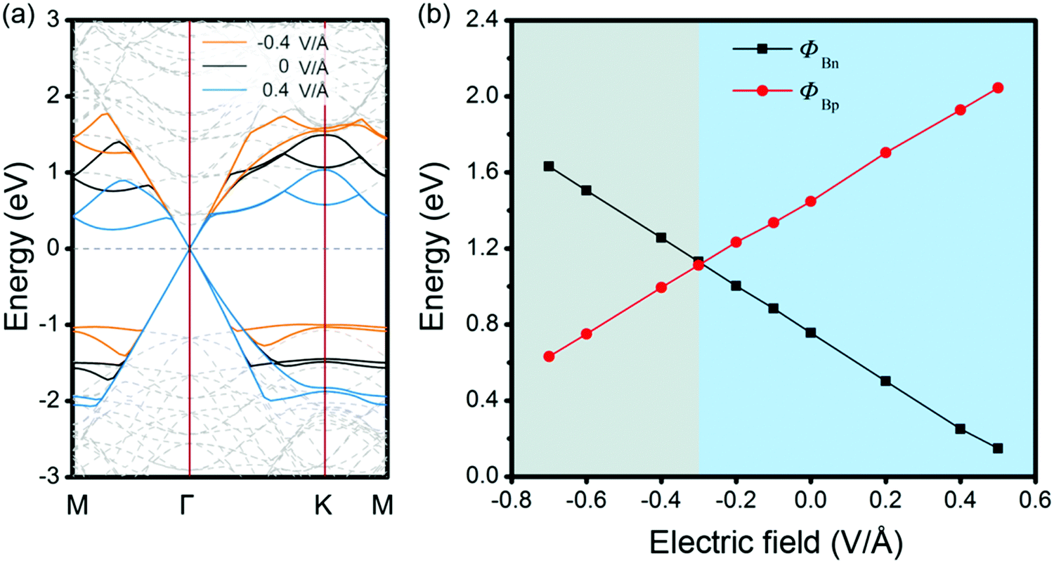 | ||
| Fig. 9 (a) Electronic band structures of MX–G under various levels of electric field. The grey lines are the contributions from MX and the colorful lines denote the contribution from G under different E-field. (b) The SBHs in MX–G as a function of the electric field. | ||
It should be noted that, GeSe/G vdW heterostructures have not been synthesized yet. However, blue-phosphorene-phase GeSe and its most stable black-phosphorene-phase are nearly degenerate in energy (the binding energy difference is within 0.025 eV per atom).38 Moreover, a similar system of blue-phosphorene-phase GeTe has been successfully synthesized through atomic layer deposition and sonication-assisted liquid-phase exfoliation methods.56,57 In particular, various mature strategies, such as mechanical stacking methods, CVD and liquid phase exfoliation techniques, etc., have been extensively developed for synthesizing G-based vdW heterostructures in experiments.30 Thus, GeSe/G vdW heterostructures are expected to be synthesized in the near future. More importantly, blue-phosphorene-phase GeSe chosen here only acts as a prototype of a series of a large number of built-in dipole systems, for example, recently fashionable Janus structures.58 Apparently, the concept of dipole-controlled SBHs is universally valid and can be extended to these kinds of charming vdW heterojunctions which are formed by stacking G and 2D materials having intrinsic dipoles.
Conclusions
In summary, we have investigated the electronic properties of GeSe/G vdW heterostructures by means of density functional theory calculations. Our results show that blue-phosphorene-phase GeSe interacts with graphene via weak vdW interactions. After forming heterostructures, their separate electronic properties are well preserved. When an X/G interface is formed, MX–G shows an n-type Schottky contact. Due to more charge transfer across the M/G interface, XM–G displays a p-type Schottky contact. By adjusting the vdW gap from non-interacting distance to equilibrium distance to less than equilibrium distance, the regulatable SBH is achieved, accompanied by the Schottky contacts of both MX–G and XM–G transition from n- to p-type. It was found that the interfacial dipole and concomitant potential step play important roles in the regulation of SBH for such heterojunctions. Interestingly, an intrinsic dipole can be used to modify the dipole of the heterostructure by stacking with multilayer GeSe, for instance, nMX–MX–G and nXM–XM–G, in which the dipole is enlarged for MX–G along the positive direction and for XM–G along the negative direction, respectively. These stackings result in the contacts changing into the Ohmic type, which is equivalent to the effect of applying an external perpendicular electric field. Our work provides a novel idea for designing G-based heterojunctions with an intrinsic dipole that SBHs are favorably controlled by stacking in different patterns. We believe that our results provide significant guidance towards potential applications of such heterostructures in novel electronic devices.Conflicts of interest
There are no conflicts to declare.Acknowledgements
This work was supported by the National Natural Science Foundation of China no. 21573002 (H. Y.) and 21705003 (D. J.), and the Fundamental Research Funds for the Central Universities (no. 30916015106). The numerical calculations in this paper have been carried out on the super-computing system in the Supercomputing Center of University of Science and Technology of China.References
- K. S. Novoselov, A. K. Geim, S. Morozov, D. Jiang, M. Katsnelson, I. Grigorieva, S. Dubonos and A. A. Firsov, Nature, 2005, 438, 197 CrossRef CAS PubMed.
- Y. Zhang, Y.-W. Tan, H. L. Stormer and P. Kim, Nature, 2005, 438, 201 CrossRef CAS PubMed.
- D. B. Farmer, H.-Y. Chiu, Y.-M. Lin, K. A. Jenkins, F. Xia and P. Avouris, Nano Lett., 2009, 9, 4474–4478 CrossRef CAS PubMed.
- X. Li, S. Yu, S. Wu, Y. Wen, S. Zhou and Z. Zhu, J. Phys. Chem. C, 2013, 117, 15347–15353 CrossRef CAS.
- C.-J. Shih, Q. H. Wang, Y. Son, Z. Jin, D. Blankschtein and M. S. Strano, ACS Nano, 2014, 8, 5790–5798 CrossRef CAS PubMed.
- C. Zhao, X. Wang, J. Kong, J. M. Ang, P. S. Lee, Z. Liu and X. Lu, ACS Appl. Mater. Interfaces, 2016, 8, 2372–2379 CrossRef CAS PubMed.
- L. Britnell, R. Gorbachev, R. Jalil, B. Belle, F. Schedin, A. Mishchenko, T. Georgiou, M. Katsnelson, L. Eaves and S. Morozov, Science, 2012, 335, 947–950 CrossRef CAS PubMed.
- Y. Ma, Y. Dai, M. Guo, C. Niu and B. Huang, Nanoscale, 2011, 3, 3883–3887 RSC.
- J. A. Miwa, M. Dendzik, S. S. Grønborg, M. Bianchi, J. V. Lauritsen, P. Hofmann and S. Ulstrup, ACS Nano, 2015, 9, 6502–6510 CrossRef CAS PubMed.
- L. Yu, Y.-H. Lee, X. Ling, E. J. Santos, Y. C. Shin, Y. Lin, M. Dubey, E. Kaxiras, J. Kong and H. Wang, Nano Lett., 2014, 14, 3055–3063 CrossRef CAS PubMed.
- K. Roy, M. Padmanabhan, S. Goswami, T. P. Sai, G. Ramalingam, S. Raghavan and A. Ghosh, Nat. Nanotechnol., 2013, 8, 826 CrossRef CAS PubMed.
- Y. Gao, R.-J. Shiue, X. Gan, L. Li, C. Peng, I. Meric, L. Wang, A. Szep, D. Walker Jr and J. Hone, Nano Lett., 2015, 15, 2001–2005 CrossRef CAS PubMed.
- R. Balu, X. Zhong, R. Pandey and S. P. Karna, Appl. Phys. Lett., 2012, 100, 052104 CrossRef.
- E. Kan, H. Ren, F. Wu, Z. Li, R. Lu, C. Xiao, K. Deng and J. Yang, J. Phys. Chem. C, 2012, 116, 3142–3146 CrossRef CAS.
- J. Sławińska, I. Zasada and Z. Klusek, Phys. Rev. B: Condens. Matter Mater. Phys., 2010, 81, 155433 CrossRef.
- Z. Liu, L. Song, S. Zhao, J. Huang, L. Ma, J. Zhang, J. Lou and P. M. Ajayan, Nano Lett., 2011, 11, 2032–2037 CrossRef CAS PubMed.
- H. Phuc, H. Nguyen, B. D. Hoi and C. Nguyen, Phys. Chem. Chem. Phys., 2018, 20, 17899–17908 RSC.
- Z. Ben Aziza, H. Henck, D. Pierucci, M. G. Silly, E. Lhuillier, G. Patriarche, F. Sirotti, M. Eddrief and A. Ouerghi, ACS Nano, 2016, 10, 9679–9686 CrossRef CAS PubMed.
- X. Li, L. Basile, B. Huang, C. Ma, J. Lee, I. V. Vlassiouk, A. A. Puretzky, M.-W. Lin, M. Yoon and M. Chi, ACS Nano, 2015, 9, 8078–8088 CrossRef CAS PubMed.
- C. Si, Z. Lin, J. Zhou and Z. Sun, 2D Mater., 2016, 4, 015027 CrossRef.
- Z. B. Aziza, D. Pierucci, H. Henck, M. G. Silly, C. David, M. Yoon, F. Sirotti, K. Xiao, M. Eddrief and J.-C. Girard, Phys. Rev. B, 2017, 96, 035407 CrossRef.
- Y. Li, J. Wang, B. Zhou, F. Wang, Y. Miao, J. Wei, B. Zhang and K. Zhang, Phys. Chem. Chem. Phys., 2018, 20, 24109–24116 RSC.
- K. D. Pham, N. N. Hieu, H. V. Phuc, B. D. Hoi, V. V. Ilysov, B. Amin and C. V. Nguyen, Comput. Mater. Sci., 2018, 153, 438–444 CrossRef CAS.
- Y. Cai, G. Zhang and Y.-W. Zhang, J. Phys. Chem. C, 2015, 119, 13929–13936 CrossRef CAS.
- J. Padilha, A. Fazzio and A. J. da Silva, Phys. Rev. Lett., 2015, 114, 066803 CrossRef CAS PubMed.
- J. Sun, H.-W. Lee, M. Pasta, H. Yuan, G. Zheng, Y. Sun, Y. Li and Y. Cui, Nat. Nanotechnol., 2015, 10, 980 CrossRef CAS PubMed.
- W. Hu, T. Wang and J. Yang, J. Mater. Chem. C, 2015, 3, 4756–4761 RSC.
- J. Zhu, J. Zhang and Y. Hao, Jpn. J. Appl. Phys., 2016, 55, 080306 CrossRef.
- M. Sun, J.-P. Chou, J. Yu and W. Tang, Phys. Chem. Chem. Phys., 2017, 19, 17324–17330 RSC.
- P. Solís-Fernández, M. Bissett and H. Ago, Chem. Soc. Rev., 2017, 46, 4572–4613 RSC.
- J. Bardeen, Phys. Rev., 1947, 71, 717 CrossRef.
- S. Tongay, T. Schumann, X. Miao, B. Appleton and A. Hebard, Carbon, 2011, 49, 2033–2038 CrossRef CAS.
- W. Xiong, C. Xia, X. Zhao, T. Wang and Y. Jia, Carbon, 2016, 109, 737–746 CrossRef CAS.
- L. Li, Y. Yu, G. J. Ye, Q. Ge, X. Ou, H. Wu, D. Feng, X. H. Chen and Y. Zhang, Nat. Nanotechnol., 2014, 9, 372 CrossRef CAS PubMed.
- J. L. Zhang, S. Zhao, C. Han, Z. Wang, S. Zhong, S. Sun, R. Guo, X. Zhou, C. D. Gu and K. D. Yuan, Nano Lett., 2016, 16, 4903–4908 CrossRef CAS PubMed.
- H. Liu, A. T. Neal, Z. Zhu, Z. Luo, X. Xu, D. Tománek and P. D. Ye, ACS Nano, 2014, 8, 4033–4041 CrossRef CAS PubMed.
- L. C. Gomes and A. Carvalho, Phys. Rev. B: Condens. Matter Mater. Phys., 2015, 92, 085406 CrossRef.
- T. Hu and J. Dong, Phys. Chem. Chem. Phys., 2016, 18, 32514–32520 RSC.
- P. E. Blöchl, Phys. Rev. B: Condens. Matter Mater. Phys., 1994, 50, 17953 CrossRef.
- J. P. Perdew, J. A. Chevary, S. H. Vosko, K. A. Jackson, M. R. Pederson, D. J. Singh and C. Fiolhais, Phys. Rev. B: Condens. Matter Mater. Phys., 1992, 46, 6671 CrossRef CAS.
- J. P. Perdew and Y. Wang, Phys. Rev. B: Condens. Matter Mater. Phys., 1992, 45, 13244 CrossRef.
- G. Kresse and J. Furthmüller, Phys. Rev. B: Condens. Matter Mater. Phys., 1996, 54, 11169 CrossRef CAS.
- S. Grimme, J. Comput. Chem., 2006, 27, 1787–1799 CrossRef CAS PubMed.
- J. Heyd and G. E. Scuseria, J. Chem. Phys., 2004, 121, 1187–1192 CrossRef CAS PubMed.
- Y. Ji, M. Yang, H. Dong, T. Hou, L. Wang and Y. Li, Nanoscale, 2017, 9, 8608–8615 RSC.
- T. Björkman, A. Gulans, A. V. Krasheninnikov and R. M. Nieminen, Phys. Rev. Lett., 2012, 108, 235502 CrossRef PubMed.
- L. Liu, J. Park, D. A. Siegel, K. F. McCarty, K. W. Clark, W. Deng, L. Basile, J. C. Idrobo, A.-P. Li and G. Gu, Science, 2014, 343, 163–167 CrossRef CAS PubMed.
- C. Xia, Q. Gao, W. Xiong, J. Du, X. Zhao, T. Wang, Z. Wei and J. Li, J. Mater. Chem. C, 2017, 5, 7230–7235 RSC.
- W. Hu, Z. Li and J. Yang, J. Chem. Phys., 2013, 139, 154704 CrossRef PubMed.
- W. Hu, T. Wang, R. Zhang and J. Yang, J. Mater. Chem. C, 2016, 4, 1776–1781 RSC.
- Y. Ren, X. Deng, Z. Qiao, C. Li, J. Jung, C. Zeng, Z. Zhang and Q. Niu, Phys. Rev. B: Condens. Matter Mater. Phys., 2015, 91, 245415 CrossRef.
- E. Abad, Y. J. Dappe, J. I. Martínez, F. Flores and J. Ortega, J. Chem. Phys., 2011, 134, 044701 CrossRef CAS PubMed.
- J. Heyd, J. E. Peralta, G. E. Scuseria and R. L. Martin, J. Chem. Phys., 2005, 123, 174101 CrossRef PubMed.
- C. Xia, B. Xue, T. Wang, Y. Peng and Y. Jia, Appl. Phys. Lett., 2015, 107, 193107 CrossRef.
- J. Neugebauer and M. Scheffler, Phys. Rev. B: Condens. Matter Mater. Phys., 1992, 46, 16067 CrossRef CAS.
- T. Gwon, T. Eom, S. Yoo, H.-K. Lee, D.-Y. Cho, M.-S. Kim, I. Buchanan, M. Xiao, S. Ivanov and C. S. Hwang, Chem. Mater., 2016, 28, 7158–7166 CrossRef CAS.
- P. Zhang, F. Zhao, P. Long, Y. Wang, Y. Yue, X. Liu, Y. Feng, R. Li, W. Hu, Y. Li and W. Feng, Nanoscale, 2018, 10, 15989–15997 RSC.
- A.-Y. Lu, H. Zhu, J. Xiao, C.-P. Chuu, Y. Han, M.-H. Chiu, C.-C. Cheng, C.-W. Yang, K.-H. Wei, Y. Yang, Y. Wang, D. Sokaras, D. Nordlund, P. Yang, D. A. Muller, M.-Y. Chou, X. Zhang and L.-J. Li, Nat. Nanotechnol., 2017, 12, 744 CrossRef CAS PubMed.
Footnote |
| † Electronic supplementary information (ESI) available. See DOI: 10.1039/c8nh00413g |
| This journal is © The Royal Society of Chemistry 2019 |