
Low-cost writing method for self-powered paper-based UV photodetectors utilizing Te/TiO2 and Te/ZnO heterojunctions
Yong
Zhang†
,
Wenxin
Xu†
,
Xiaojie
Xu
,
Wei
Yang
,
Siyuan
Li
,
Jiaxin
Chen
and
Xiaosheng
Fang
 *
*
Department of Materials Science, Fudan University, Shanghai 200433, China. E-mail: xshfang@fudan.edu.cn
First published on 28th November 2018
Abstract
It has always been a challenge to prepare self-powered ultraviolet photodetectors (UV PDs) utilizing a green, facile and low-cost method. Here, we provide such an approach for fabricating self-powered photodetectors based on Te nanowire/TiO2 nanoparticle (NP) and Te nanowire/ZnO nanoparticle (NP) heterojunctions. It is noteworthy that such devices were prepared via simply brushing non-toxic solution-processed Te nanowires and commercial TiO2 and ZnO nanoparticles onto paper. The as-obtained UV PDs can work under zero bias due to photovoltaic effects from the Te/TiO2 and Te/ZnO heterojunctions. This study not only presents high-performance UV PDs, but also provides a general and effective method for developing environmentally-friendly and energy-efficient optoelectronic devices for practical applications. The concept of employing daily-use brushes and recyclable paper provides a facile way to fabricate green low-cost PDs.
Conceptual insightsTo make electronic devices simpler and greener, writing is becoming a popular method. Paper can be written on and recycled and is environmentally-friendly. Considering the simplicity, low cost and low energy consumption, using paper as a substrate and a brush as a tool to form low-cost self-powered PDs is worth exploring. In this paper, Te nanowires are synthesized via a low-cost green process and commercial TiO2 (ZnO) NPs are low-cost. UV PDs based on Te/TiO2 (ZnO) are developed via a writing method using brushes and paper. The as-obtained UV PDs can work under zero bias due to photovoltaic effects from the heterojunction. These results lay solid groundwork for future research into Te-based heterojunction PDs. More importantly, the concept of employing daily-use brushes and recyclable paper provides a facile way to fabricate green low-cost PDs. |
Introduction
Ultraviolet photodetectors (UV PDs) have attracted much attention in both academia and industry in the past few decades due to their applications in versatile fields including environmental monitoring,1–3 flame sensing,4,5 missile warning systems,6etc. Differing from devices that can only operate under an external power source, self-powered PDs can work under zero bias due to photovoltaic effects from p–n junctions or heterojunctions under illumination.7,8 Such self-powered characteristics have been urgently pursued in electronic devices, especially when facing the energy crisis era. As for UV PDs, self-powered examples have shown great potential in chemical and biological analysis and communications, as they are effective, reliable and energy-saving.9,10Te, a p-type semiconductor with wide ranging applications in photoconductive detection and nonlinear optics,11–13 is a promising candidate for photodetection. In hexagonal Te, highly anisotropic helical chains exist, making it easy to grow one dimensional Te nanostructures such as nanowires and nanotubes, even without templates or surfactants to induce anisotropic growth.14 Consequently, the process of synthesizing Te nanowires can be simple, fast and high-yield. Te nanowires have a large specific surface area and good charge transport properties, which can produce high current gain. Meanwhile, Te nanowires have strong metallicity, with high electrical conductivity of ∼3.04 S M−1, although Te is a nonmetallic rare element.15,16 N-Type titanium dioxide (TiO2) is a well-studied and commercialized semiconductor with a large band gap corresponding to the UV region. However, there are no reports on UV PDs based on a Te/TiO2 heterojunction. Therefore, there is a need to explore Te/TiO2 devices to probe the possibilities of self-powered UV PDs.
To make electronic devices simpler and greener, writing is becoming a popular method. ZnO NPs have been mixed with graphene, compressed into a pencil and used to directly write on paper to prepare optoelectronic devices.17,18 A micropipette has been employed to form arched PDs based on PbS quantum dots/P3HT hybrid nanowires via direct hand writing.19 However, the above mentioned techniques are expensive, with requirements for special facilities or conditions. Paper, a great human invention that is made of vegetable fibers and can be written on and recycled, is environmentally friendly. To date, raw paper has been demonstrated as a carrier of ZnO PDs.20 However, to the best of our knowledge, they have shown no self-powered characteristics that can further reduce energy consumption and meet the trend of improving energy efficiency. Considering the simplicity, low-cost and low energy consumption, using paper as a substrate and a brush as a tool to form low-cost self-powered UV PDs with high performance is worth exploring.
In this work, Te nanowires are obtained via a simple and green hydrothermal method. Te nanowires and commercial TiO2 (ZnO) NPs dispersed in ethanol are transferred onto paper using a writing brush. Subsequently, a self-powered photodetector with an overlapping Te and TiO2 (ZnO) structure is obtained. Thus, a simple and low-cost, general and green approach for creating self-powered PDs is introduced.
Results and discussion
Fig. 1a–c shows X-ray diffraction (XRD) patterns of Te nanowires, TiO2 and ZnO NPs, respectively. All the peak positions of the Te nanowires and the relative intensities are in good agreement with a hexagonal tellurium phase with lattice parameters of a = b = 4.458 Å and c = 5.927 Å (JCPDF No. 36-1452), confirming the good crystallinity and purity of the as-obtained sample (Fig. 1a). The main diffraction peaks of the Te nanowires located at 23.0°, 38.3° and 40.4° are attributed to the (100), (102) and (110) crystal planes. The remarkable sharp peak at 27.6° indicates that the growth direction of the Te nanowires is mainly along the (101) direction. The diffraction peaks of the TiO2 NPs indicate the existence mainly of an anatase phase (JCPDF No. 21-1272) with a little of a rutile phase (JCPDF No. 21-1276) (Fig. 1b). The sharp peak of TiO2 NPs located at 25.3° is assigned to the (101) plane of the anatase phase of TiO2. The weak diffraction peak with a 2θ value of 27.4° is indexed to the (110) crystal facet of a rutile phase. For the ZnO NPs, the diffraction peaks with 2θ values of 31.8°, 34.4°, and 36.3° are indexed to the (100), (002), and (101) crystal facets of ZnO (JCPDF No. 65-3411) (Fig. 1c).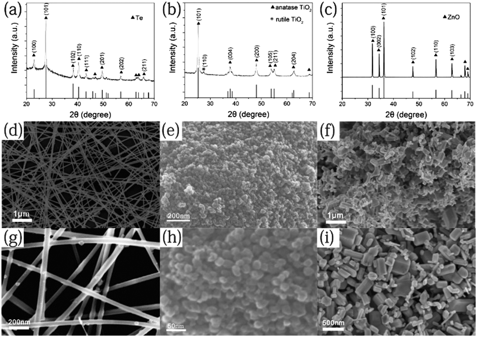 | ||
| Fig. 1 XRD patterns of (a) Te nanowires; (b) TiO2 nanoparticles; and (c) ZnO nanoparticles. SEM images of (d and g) Te nanowires; (e and h) TiO2 nanoparticles; and (f and i) ZnO nanoparticles. | ||
Fig. 1d–i displays scanning electron microscopy (SEM) images of the three samples at different magnifications. In Fig. 1d and g, Te nanowires with a mean diameter of 30–60 nm and length of more than 10 μm are observed. The aspect ratio is in the range of 150–350, which shows the anisotropy of the Te products and indicates the preferential growth direction of (101). The surfaces are smooth, indicating the high purity and quality of the Te nanowires. The TiO2 NPs, with an average diameter of less than 100 nm, are observed as agglomerating together, as shown in Fig. 1e and h. The images of the cuboid ZnO NPs in Fig. 1f and i, demonstrate that the sizes of the nanoparticles are mainly in the range of 200–300 nm and that they are densely packed. The morphologies and sizes match well with those of commercial TiO2 and ZnO NPs.
Fig. 2a presents a schematic diagram of the Te/TiO2 UV PD. The Te nanowires and commercial TiO2 NPs are dispersed in ethanol to form an ink and then transferred onto filter paper using two brushes. The rough surface of the filter paper allows the ethanol to be easily absorbed and quickly volatilized, leaving the particles attached to the paper. Indium paste was used as the electrodes and the optoelectronic properties of the Te/TiO2 UV PD were investigated at room temperature. Fig. 2b shows typical current–voltage (I–V) curves from the Te/TiO2 UV PD as logarithmic plots in the dark and upon 350 nm UV illumination. The dark current under a bias of 0 V is 0.02 nA and under a forward bias of 0.5 V is 0.5 nA; this shows an unsymmetrical response for forward and reverse biases. The values for the photocurrent under 350 nm light at biases of −0.5, 0 and 0.5 V are estimated to be 0.01, 1, and 2 nA, respectively. Notably, the photocurrents are lower than the dark currents when the bias is lower than −0.25 V, with the lowest photocurrent occurring at −0.5 V, while the photocurrents are higher than the dark current at +0.5 V. This interesting feature will be elaborated on later. The relatively high photocurrent of 1 nA existing at a nominal zero bias indicates that the hybrid device can operate without an external bias. In comparison, I–V curves for a pristine TiO2 device and pure Te device are shown in Fig. 2c and d, respectively. The pure TiO2 PD shows a noticeable photoresponse, while the pure Te PD shows no obvious photoelectric properties. The dark current and the photocurrent indicate that neither pure TiO2 nor Te PDs are able to generate such self-powered behavior. Thus, it is believed that the self-powered behavior of the Te/TiO2 hybrid device mainly arises from a heterojunction formed between the Te nanowires and TiO2 NPs.
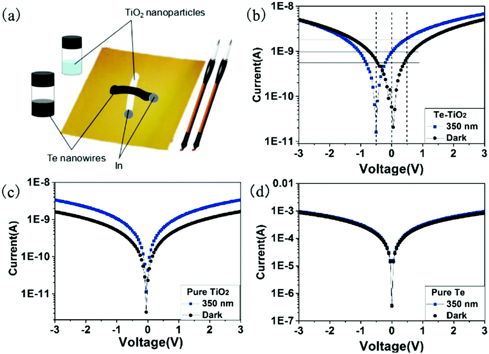 | ||
| Fig. 2 (a) A schematic diagram of the Te/TiO2 UV PD. The I–V characteristics of (b) Te/TiO2, (c) pure TiO2 and (d) pure Te photodetectors under dark conditions and when illuminated with 350 nm UV light. | ||
Fig. 3a exhibits a time-dependent current (I–t) curve of the Te/TiO2 PD upon periodic 350 nm light illumination under zero bias. After each cycle of switching on, the current instantly increases to 0.8–1.0 nA, which corresponds well with the results in Fig. 2b. The rise (decay) time is the time taken for the photocurrent to increase from 10% to 90% (drop from 90% to 10%) in the normalized curve. An enlarged graph of one on–off cycle (Fig. 3b) shows the rise time and decay time of the device. For the presented Te/TiO2 PD, the values are calculated as 0.772 s and 1.492 s. The spectral responsivity (Rλ) of a device, defined as the photocurrent per unit of incident power, is another key parameter to evaluate the performance of a PD, indicating how efficiently a detector responds to optical signals. It is usually calculated using the equation
 | (1) |
 | (2) |
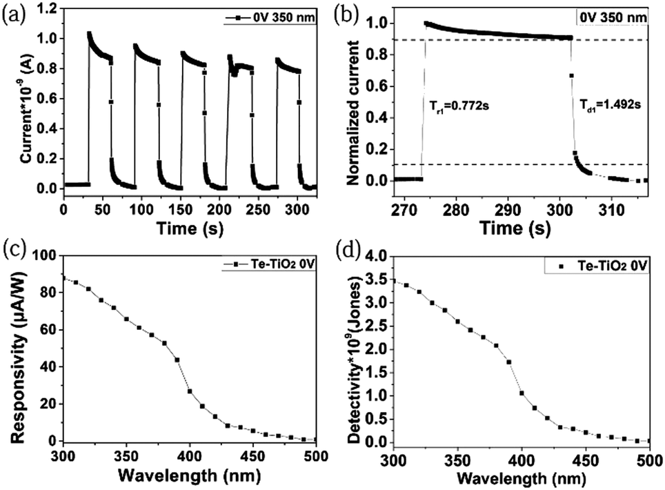 | ||
| Fig. 3 (a) The I–t curve of the Te/TiO2 PD with periodic on/off switching upon 350 nm UV light illumination under a 0 V bias. (b) The normalized I–t curve of the Te/TiO2 PD. (c) The spectral responsivity of the device under a 0 V bias. (d) The detectivity of the Te/TiO2 PD as a function of wavelength under a 0 V bias. | ||
To further explore the characteristics of the Te/TiO2 self-powered PD, we examined its binary response under +0.5 V and −0.5 V biases at a wavelength of 350 nm. As displayed in Fig. 4a, the photocurrent is higher than the dark current under +0.5 V, while lower than dark current under −0.5 V. The I–t curve under negative bias reveals that on/off switching is repeatable and stable without apparent photocurrent-decay over multiple cycles. Interestingly, the photocurrent decreases when the light is turned on and increases when the light is turned off under a −0.5 V bias, showing the opposite trend in variation to that at +0.5 V. This may result from photovoltaic effects and the photo-to-dark current ratio shown in Fig. 2b. Under a bias of −0.5 V, the dark current is at a relatively high level, while the photocurrent goes down to the lowest point. On the contrary, the Te/TiO2 PD under positive biases shares similar photoelectric properties with regular UV PDs. Fig. 4b shows that the responsivity under a bias of −0.5 V reaches up to 100 mA W−1, while under 0.5 V the value of Rλ rises to 125 mA W−1.
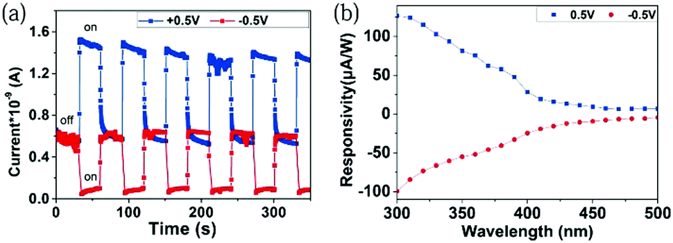 | ||
| Fig. 4 (a) I–t curves of a Te/TiO2 PD with periodic on/off switching upon 350 nm UV light illumination under 0.5 V and −0.5 V biases; and (b) the spectral responsivity. | ||
To demonstrate the effectiveness and generality of this writing method to prepare self-powered UV PDs, Te/ZnO devices are also examined, as shown in Fig. 5. Like TiO2, ZnO has been well-explored for use in UV PDs. As displayed in Fig. 5c, pure ZnO shows no self-powered response, though it presents a large photo-to-dark current ratio. Comparing the results in Fig. 2d and 5a, it is indicated that a typical Te/ZnO PD shows self-powered behavior, which originates from a heterojunction between Te nanowires and ZnO NPs. Fig. 5b shows that the current under 350 nm at 0 V reaches ∼0.5 nA immediately when the light is switched on, and the photocurrent grows stepwise as the on/off cycling continues. The on–off ratio is close to 100. Notably, the response times of the Te/ZnO PD are quick. As shown in Fig. 5d, the rise time and decay time of the device are 2.46 s and 1.75 s, respectively. The fast response to light illumination is significant for high performance PDs. Fig. 5e demonstrates that the responsivity of the Te/ZnO hybrid device is close to 7 μA W−1 in the wavelength range of 400–500 nm but rapidly rises with a reduction of wavelength and reaches a value of 387 mA W−1 at a wavelength of 300 nm. The detectivity variation trend matches well with the responsivity, with the highest value of 4 × 10¹⁰ Jones occurring at a wavelength of 300 nm (Fig. 5f). These results are close to those for Te/TiO2 UV PDs. The self-powered features of the as-prepared UV PDs are discussed as follows. As shown in Fig. 6, p type Te (∼0.34 eV) and n type TiO2 (∼3.2 eV) or ZnO (∼3.37 eV) produce a typical Type II heterojunction.21–23 Under UV-light illumination, photogenerated electrons and holes will be quickly separated by the built-in electric field.24
 | ||
| Fig. 5 I–V curves of the (a) Te/ZnO PD and (c) pure ZnO under dark conditions and illumination with 350 nm UV light. (b) The I–t curve of the Te/ZnO PD with periodic on/off switching upon 350 nm light illumination under a 0 V bias. (d) The normalized I–t curve of the Te/ZnO PD. (e and f) The spectral responsivity and detectivity of Te/ZnO PD as a function of wavelength under a 0 V bias. | ||
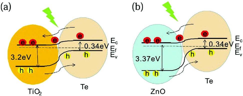 | ||
| Fig. 6 Schematic energy-band diagrams of the (a) Te/TiO2 and (b) Te/ZnO PDs, showing the photogenerated carrier transfer process under UV illumination. | ||
The anisotropy of Te makes it easier to form one dimensional nanostructures. This structure-determined nature makes Te an appealing candidate for versatile applications, especially for PDs, where the mechanism explained above may be applied to other Te-based PDs to gain attractive self-powered features. Meanwhile, the writing method introduced in this article may also be employed in the fabrication of other optoelectronic devices. In addition, brushes may even be used to transfer nanomaterials to form pictures, displaying the high controllability of fabricating devices in different shapes. It is also possible to substitute paper for other deformable materials, like cloth and plastic bags. Compared with other processes, including spin-coating, annealing or growing arrays,25–30 writing is more efficient, energy saving and low-cost. Compared with pressed pencils17,18 which require expensive facilities and special conditions, brushes are low-cost. This architecture may result in more ways to manufacture electronic devices.
Conclusions
In summary, Te nanowires are synthesized via a low-cost, green, hydrothermal process. Commercial TiO2 NPs are also low-cost. UV PDs based on Te/TiO2 are developed via a writing method using brushes and paper. This approach is so simple and effective that TiO2 can be substituted by other n-type materials, such as ZnO, without compromising on performance. The built-in field at the heterojunction of Te and TiO2 or ZnO allows the device to operate without an external power supply. Both UV PDs are energy-saving, and the photocurrents of both PDs at 0 V reach up to 1 nA. The results reported in this work lay solid groundwork for future research into Te-based heterojunction PDs with excellent power-to-cost ratios, high signal-to-noise ratios and good spectral selectivities. More importantly, the simple and green writing method for fabricating low-cost self-powered UV PDs can be applied to more practical studies, showing promise for future applications in biomedical sensors, mobile devices and so on.Experimental section
Preparation of Te nanowires
All reagents purchased from Aladdin were directly used without further treatment. Firstly, 0.165 g of TeO2, 0.167 g of KOH and 30 mL of glycol were added to a 100 mL beaker, and then heated to 85 °C under stirring. After a transparent solution was obtained, 0.1 g of PVP (K30) was added under continuous stirring. Then 1.5 mL of ascorbic acid was added to the solution. The solution was stirred until it turned yellow and it was transferred to a Teflon-lined stainless steel autoclave. The sealed autoclave was kept for 6 hours at 150 °C and was then naturally cooled to room temperature. The product was separated using high-speed centrifugation and then was rinsed with absolute alcohol and acetone three times. Finally, the product was dispersed in alcohol for the next step of composition.Fabrication of Te/TiO2 and Te/ZnO composites
150 mg of TiO2 NPs (purity 99.8%, 60 nm, anatase) or ZnO NPs (purity 99.9%, 200 nm), purchased from Aladdin, were dispersed in 5 mL of ethanol. The devices were prepared using a Chinese brush. We painted a line of TiO2 or ZnO NPs on certain substrates, such as filter paper, and then a line of Te ink was added perpendicularly and linked to the former line. After the volatilization of ethanol, the PDs were obtained.Material characterization
Sample morphologies were characterized using FE-SEM (Zeiss Sigma). XRD patterns were collected using a Bruker D8-A25 diffractometer using Cu Kα radiation (l = 1.5405 Å) over a 2θ range from 20° to 70°. To construct the photodetectors, two small pieces of indium paste with areas approximating 0.1 cm2 were doctor-bladed onto the composite films as electrodes. The photoelectric performances were characterized using a program-controlled semiconductor characterization system (Keithley 4200, USA). The light intensity was measured with a NOVA II power meter (OPHIR Photonics). All measurements were conducted under ambient conditions.Conflicts of interest
The authors declare no conflicts of interest.Acknowledgements
This work was supported by the National Key Research and Development Program of China (2017YFA0204600), the National Postdoctoral Science Foundation of China (2017M621355), the National Natural Science Foundation of China (Grant No. 51721002, 51872050, 11674061 and 51471051), the Science and Technology Commission of Shanghai Municipality (18520710800, 17520742400, and 15520720700), the Programs for Professors of Special Appointment (Eastern Scholar) at Shanghai Institutions of Higher Learning, and the National Program for the Support of Top-notch Young Professionals. Part of the experimental work was carried out in the Fudan Nanofabrication Laboratory.Notes and references
- H. Y. Chen, H. Liu, Z. M. Zhang, K. Hu and X. S. Fang, Adv. Mater., 2016, 28, 403 CrossRef CAS.
- G. Chen, B. Liang, X. Liu, Z. Liu, G. Yu, X. Xie, T. Luo, D. Chen, M. Q. Zhu, G. Z. Shen and Z. Y. Fan, ACS Nano, 2014, 8, 787 CrossRef CAS.
- Y. Ning, Z. M. Zhang, F. Teng and X. S. Fang, Small, 2018, 14, 1703754 CrossRef PubMed.
- W. Tian, Y. D. Wang, L. Chen and L. Li, Small, 2017, 13, 1701848 CrossRef PubMed.
- M. H. Zarifi, B. Wiltshire, N. Mahdi, P. Kar, K. Shankar and M. Daneshmand, Nanoscale, 2018, 10, 4882 RSC.
- W. X. Ouyang, F. Teng and X. S. Fang, Adv. Funct. Mater., 2018, 28, 1707178 CrossRef.
- S. M. Hatch, J. Briscoe and S. Dunn, Adv. Mater., 2012, 25, 867 CrossRef PubMed.
- F. Teng, K. Hu, W. X. Ouyang and X. S. Fang, Adv. Mater., 2018, 30, 1706262 CrossRef.
- B. S. Ouyang, K. W. Zhang and Y. Yang, Adv. Mater. Technol., 2017, 2, 1700208 CrossRef.
- X. J. Xu, S. Li, J. Chen, S. Cai, Z. Long and X. S. Fang, Adv. Funct. Mater., 2018, 28, 1802029 CrossRef.
- K. Zhang and S. Wang, Carbon, 2014, 69, 46 CrossRef CAS.
- G. Zhang, H. Fang, H. Yang, L. A. Jauregui, Y. P. Chen and Y. Wu, Nano Lett., 2012, 12, 3627 CrossRef CAS PubMed.
- M. Amani, C. L. Tan, G. Zhang, C. S. Zhao, J. Bullock, X. H. Song, H. Kim, V. R. Shrestha, Y. Gao, K. B. Crozier, M. Scott and A. Javey, ACS Nano, 2018, 12, 7253 CrossRef CAS PubMed.
- H. Zhu, H. Zhang, J. Liang, G. Rao, J. Li, G. Liu, Z. Du, H. Fan and J. Luo, J. Phys. Chem. C, 2011, 115, 6375 CrossRef CAS.
- J. W. Liu, J. H. Zhu, C. L. Zhang, H. W. Liang and S. H. Yu, J. Am. Chem. Soc., 2010, 132, 8945 CrossRef CAS.
- H. H. Li, P. Zhang, C. L. Liang, J. Yang, M. Zhou, X. H. Lu and G. A. Hope, Cryst. Res. Technol., 2012, 47, 1069 CrossRef CAS.
- R. S. Veerla, P. Sahatiya and S. Badhulika, J. Mater. Chem. C, 2017, 5, 10231 RSC.
- L. X. Zheng, K. Hu, F. Teng and X. S. Fang, Small, 2016, 13, 1602448 CrossRef.
- J. Yoo, S. Jeong, S. Kim and J. H. Je, Adv. Mater., 2015, 27, 1712 CrossRef CAS.
- C. H. Lin, D. S. Tsai, T. C. Wei, D. H. Lien, J. J. Ke, C. H. Su, J. Y. Sun, Y. C. Liao and J. H. He, ACS Nano, 2017, 11, 10230 CrossRef CAS.
- D. Iqbal, A. Sarfraz and A. Erbe, Nanoscale Horiz., 2018, 3, 58 RSC.
- K. Hu, F. Teng, L. X. Zheng, P. P. Yu, Z. M. Zhang, H. Y. Chen and X. S. Fang, Laser Photonics Rev., 2017, 11, 1600257 CrossRef.
- X. S. Fang, L. F. Hu, C. H. Ye and L. D. Zhang, Pure Appl. Chem., 2010, 82, 2185 CAS.
- L. X. Su, W. Yang, J. Cai, H. Y. Chen and X. S. Fang, Small, 2017, 13, 1701687 CrossRef.
- J. Cai, J. Huang, M. Ge, J. Iocozzia, Z. Lin, K. Zhang and Y. Lai, Small, 2017, 13, 1604240 CrossRef.
- J. M. Song, Y. Z. Lin, Y. J. Zhan, Y. C. Tian, G. Liu and S. H. Yu, Cryst. Growth Des., 2008, 8, 1902 CrossRef CAS.
- H. Y. Chen, K. W. Liu, L. F. Hu, A. A. Al-Ghamdi and X. S. Fang, Mater. Today, 2015, 18, 493 CrossRef CAS.
- X. Huang, Y. Q. Yu, T. Jones, H. Fan, L. Wang, J. Xia, Z. J. Wang, L. D. Shao, X. M. Meng and M. G. Willinger, Adv. Mater., 2016, 28, 7603 CrossRef CAS.
- W. Yang, K. Hu, F. Teng, J. H. Weng, Y. Zhang and X. S. Fang, Nano Lett., 2018, 18, 4697 CrossRef CAS.
- C. Y. Nam and A. Stein, Adv. Opt. Mater., 2017, 5, 1700807 CrossRef.
Footnote |
| † These authors contributed equally to this work. |
| This journal is © The Royal Society of Chemistry 2019 |