
Unveiling exceptionally robust valley contrast in AA- and AB-stacked bilayer WS2†
Yanlong
Wang
 ab,
Chunxiao
Cong
*c,
Jingzhi
Shang
a,
Mustafa
Eginligil
d,
Yuqi
Jin
b,
Gang
Li
b,
Yu
Chen
a,
Namphung
Peimyoo
a and
Ting
Yu
*a
ab,
Chunxiao
Cong
*c,
Jingzhi
Shang
a,
Mustafa
Eginligil
d,
Yuqi
Jin
b,
Gang
Li
b,
Yu
Chen
a,
Namphung
Peimyoo
a and
Ting
Yu
*a
aDivision of Physics and Applied Physics, School of Physical and Mathematical Sciences, Nanyang Technological University, 637371, Singapore. E-mail: yuting@ntu.edu.sg
bKey Laboratory of Chemical Lasers, Dalian Institute of Chemical Physics, Chinese Academy of Sciences, Dalian 116023, China
cState Key Laboratory of ASIC & System, School of Information Science and Technology, Fudan University, Shanghai 200433, China. E-mail: cxcong@fudan.edu.cn
dKey Laboratory of Flexible Electronics (KLOFE) & Institute of Advanced Materials (IAM), Jiangsu National Synergetic Innovation Centre for Advanced Materials (SICAM), Nanjing Tech University (NanjingTech), 30 South Puzhu Road, Nanjing 211816, China
First published on 1st November 2018
Abstract
Valleytronics is a particularly interesting field that employs the valley degree of freedom for information manipulation. The fascinating prospects for realizing valleytronic devices have inspired persistent efforts towards exploring material systems with robust valley polarization. Monolayer transition metal dichalcogenides (TMDs) obey the well-known valley-dependent selection rule as a result of their inversion asymmetry. However, for inversion-symmetric bilayer tungsten-based TMDs, highly selective valley polarization has been surprisingly observed and is not yet fully understood. Here we systematically study the origin of the anomalously high valley polarization in bilayer WS2 by temperature-dependent polarization-resolved photoluminescence measurements. It is found that acoustic phonons play a critical role in the valley polarization of bilayer WS2. For some WS2 bilayers with relatively small intensity ratios of indirect to direct bandgap emission, acoustic phonons could remarkably assist the intervalley scattering process and smear the valley contrast. On the other hand, in other bilayers, which show obvious indirect band gap emission, the indirect optical transition process depletes the phonon mode at the Λ point dramatically and results in anomalously robust valley polarization in bilayer WS2. These results help recognize the crucial role of electron–phonon coupling in intervalley relaxation in bilayer WS2 and provide new insights into the future design of valleytronic devices based on two-dimensional TMDs.
Conceptual insightsValleytronics has emerged as a particularly interesting field and shows fascinating prospects for realizing valleytronic devices. Monolayer transition metal dichalcogenides (TMDs) possess valley polarization as a result of their inversion asymmetry, which makes them promising for next-generation valleytronics. For bilayer TMDs with tunable interlayer interaction, valley polarization is more desirable and experimentally observed to be even larger than the monolayer counterpart in WS2 with inversion symmetry. However, the exact mechanism of the robust valley polarization in bilayers remains unknown, which greatly limits the development of valleytronic devices based on TMDs. We, for the first time, report the correlation between the intensity of the indirect bandgap emission and valley polarization. We have demonstrated that acoustic phonons play a leading role in the valley polarization of bilayer WS2 and the depletion of such phonons in the indirect optical transition process could contribute to the exceptionally robust valley polarization. The observed tunable valley polarization by interlayer coupling not only sheds light on the critical role of electron–phonon coupling in the intervalley scattering process in bilayer WS2, but also provides guidance for enhancing the valley contrast in few-layer TMDs, both of which are essential for the future development of novel valleytronic devices based on two-dimensional materials. |
Introduction
Two-dimensional (2D) group-VIB transition metal dichalcogenides (TMDs) have generated considerable research interest in recent years for both fundamental studies and application prospects as a result of their inherent energy gaps and numerous other promising features such as the transformation from the indirect to direct bandgap when approaching the monolayer limit.1–9 In particular, semiconducting TMDs with the general formula of MX2 (M represents Mo or W and X represents S or Se)6,10 are considered interesting candidates for achieving valleytronics,11,12 a rather interesting field where the valley degree of freedom is explored as an information carrier.13 In monolayer TMDs, there exist inequivalent and energetically degenerate valleys at K and K′ points in the hexagonal Brillouin zone.14–16 It has been predicted that interband transitions obey the valley-dependent optical selection rule in non-centrosymmetric monolayer TMDs.17–20 More specifically, the direct bandgap transitions at K (K′) exclusively couple to σ+ (σ−) circularly polarized light.6,10 This valley-contrasted circular polarization, together with the large separation between K and K′ points in the momentum space, makes the valley serve as another robust index of charge carriers in addition to spin.20 Valley polarization could be detected by measuring the circular states of photoluminescence (PL) after selective optical pumping and the expected circular dichroism has been observed in monolayer TMDs in this way.14–16,21,22In bilayer TMDs with inversion symmetry, the valley-dependent selection rule does not apply anymore and low valley contrast was observed in AB-stacked bilayer MoS2,15,23,24 which greatly restricts the range of thickness selection for achieving potential MoS2-based valleytronics. In contrast to MoS2 with comparable spin-valley coupling and interlayer hopping energy, the significantly higher spin-valley coupling strength in bilayer tungsten-based TMDs (WX2) leads to suppressed interlayer hopping. Therefore, WX2 bilayers possess an extra index called layer polarization in addition to valley and spin indices, which could provide information on the location of charge carriers (either top-layer or bottom-layer).14,25 The giant spin–layer–valley coupling paves a new way to manipulation of the electronic degrees of freedom in WX2.14,25 Excitingly and surprisingly, highly selective circular polarization has been reported for the direct transition in centrosymmetric bilayer WS2 and WSe2,14,26,27 which is not only contrary to the widely accepted anticipation that valley-induced circular polarization should be inherently absent in centrosymmetric materials, but also shows an even larger valley contrast value than that of the monolayer,14,26 indicating that bilayer WX2 is a fascinating platform for further exploration of valley physics.18 However, the unexceptionally large valley contrast in bilayer WX2 is far from being well understood and deserves further investigation. The anomalous valley property was attributed to either localization of spin polarization in each individual layer by Liu et al.28 or suppressed interlayer hopping as a result of large spin-valley coupling compared to the interlayer hopping amplitude by Zhu et al. in bilayer WX2.14,25 Though these explanations provide valuable information that valley polarization is not only limited to noncentrosymmetric systems in WX2, why the valley polarization in bilayer WX2 could be obviously larger than that in the monolayer counterpart14,27 still cannot be explained from either of these two viewpoints and remains to be elucidated.
Interlayer coupling has been shown to significantly tune the optical properties of bilayer WX2.29,30 However, up to now, the experimental studies of valley properties have been limited to mechanically exfoliated (ME) bilayer WS2 samples with quite strong interlayer coupling.14,26,27 Though the interlayer coupling is expected to have a pronounced effect on valley polarization,24 systematic studies of their relationship are still lacking in bilayer WX2. A detailed study of the modulation of the valley polarization by interlayer coupling should help unveil the physics behind the unexpectedly large circular polarization in bilayer WS2 and provide new insights into the future development of valleytronic devices based on TMDs. In this work, we explore the origin of the anomalously high valley polarization in bilayer WS2 by a systematic study of samples with different polytypes and on distinct substrates fabricated by different methods. The effect of phonons on valley polarization is clearly revealed by a comparison of valley behaviors in various bilayer WS2 samples using temperature-dependent circularly polarized PL spectroscopy. Bilayer WS2 samples whose light emissions are mainly contributed by the direct-gap emission peak possess low-temperature valley contrast similar to the monolayer counterpart as a result of the suppressed interlayer hopping and the acoustic phonons are shown to be the dominant factor in assisting the intervalley scattering process. And, the depletion of such phonons in the indirect optical transition process could give rise to the exceptionally robust valley polarization in some WS2 bilayers, where indirect-gap emission contributes significantly to the overall light emission.
Results and discussion
Before we probe the circularly polarized behaviors of bilayer WS2, we first studied the effects of substrates and fabrication methods on valley contrast in monolayer WS2 as a reference. Temperature-dependent circularly polarized PL measurements were performed on three kinds of monolayer samples, i.e. chemical vapor deposition (CVD)-grown WS2 both on sapphire and on SiO2/Si substrates, and a ME one on a SiO2/Si substrate. Fig. S1 (ESI†) shows the evolution of PL spectra for the three monolayer WS2 samples from 80 to 300 K. The PL emission of monolayer WS2 consists of two components corresponding to the direct excitonic transition at the K point in the Brillouin zone: neutral excitons (A) at higher energy and trions (A−) at relatively lower energy.31,32 Though the relative spectral weights of A and A− may vary for different types of monolayer WS2 samples, they all share similar trends of A−–A spectral weight transformation with increasing temperature, which can be explained by the escape of electrons from the trion state owing to thermal fluctuations.33,34 The degree of circular polarization is calculated as26 | (1) |
We then studied the valley behaviors of bilayer WS2. When two individual layers are vertically stacked, different bilayer structures can be formed depending on the twist angle θ, among which the most stable configurations are an AA stacking sequence when θ = 0° and an AB stacking (also called Bernal stacking) sequence when θ = 60°.35 To begin with, we compared the valley behaviors of AA- and AB-stacked bilayer WS2 on SiO2/Si substrates (Fig. 1). According to the relative orientation of the two vertically stacked layers from the optical images in Fig. 1c and d, the twist angle and the corresponding stacking order can be determined.35Fig. 1a and b present the circularly polarized components of PL spectra as a function of temperature for AA- and AB-stacked bilayer WS2. The A peak dominates the PL spectra and redshifts with the increase of temperature, which is attributed to the reduction of the direct transition energy caused by the expanded in-plane lattice constant.36 As can be seen in Fig. 1e, both these two samples have similar dependences of valley contrast on temperature and the valley contrast at 80 K is close to that of the monolayer WS2 on the SiO2/Si substrate. This observation is due to the suppressed interlayer hopping in these two samples. In AB-stacked bilayer WS2, it is caused by the large spin-valley coupling of holes compared to the interlayer hopping amplitude,25,37 while the opposite spin of electrons between neighbouring layers inhibits the interlayer hopping in AA-stacked bilayer WS2.17,24,38 By increasing the integration time, the indirect bandgap peak (denoted I) corresponding to Λ–Γ transition39 could also be observed, as shown in Fig. S3 of the ESI.† Though the I peak is much broader than the A exciton peak, the integrated intensity of the former is only slightly larger than one quarter of that of the latter, which makes it difficult to resolve the I peak under the measurement conditions in Fig. 1. Since the polarization of the weak I peak in bilayer WS2 on the SiO2/Si substrate is not the focus of this paper, we did not use long integration times for the collection of PL spectra at low temperatures to avoid laser-induced damage.
 | ||
| Fig. 1 Circularly polarized behaviors of CVD-grown AA- and AB-stacked bilayer WS2 on SiO2/Si substrates. Circularly polarized components of PL spectra as a function of temperature for (a) AA- and (b) AB-stacked bilayer WS2. (c) and (d) show optical images of AA- and AB-stacked bilayer WS2 samples, respectively. (e) Temperature dependence of circular polarization for AA- and AB-stacked bilayer WS2. The excitation light is left-circularly polarized in all the measurements. | ||
To investigate the effect of the fabrication method on valley contrast in bilayer WS2, temperature-dependent circularly polarized PL measurements were performed on ME bilayer WS2. Fig. 2 shows the circularly polarized behaviors of ME bilayer WS2 on a SiO2/Si substrate as a function of temperature. Since ME bilayer WS2 was exfoliated from a bulk 2H-WS2 crystal, it is supposed to possess an AB stacking sequence.40 As shown in Fig. 2a, the obvious I peak appears over the whole temperature range and exhibits a blueshift with increasing temperature, consistent with a previous report.36 In contrast to the remarkable valley-polarized behaviors of A excitons, the I peak is circularly unpolarized at all the measured temperatures, in good agreement with a previous observation.14 A comparison of Fig. 1e and 2c shows that the valley polarization of A excitons in ME bilayer WS2 is obviously larger than that of the CVD-grown AB-stacked bilayer WS2 on the SiO2/Si substrate and can reach 64.3% at 80 K. Considering that ME monolayer WS2 shows comparable valley polarization to that of the CVD-grown monolayer WS2, the pure effect of the fabrication method on the valley polarization of individual layers can be excluded and intervalley scattering may possibly be weakened by the interlayer coupling in ME bilayer WS2 on the SiO2/Si substrate.
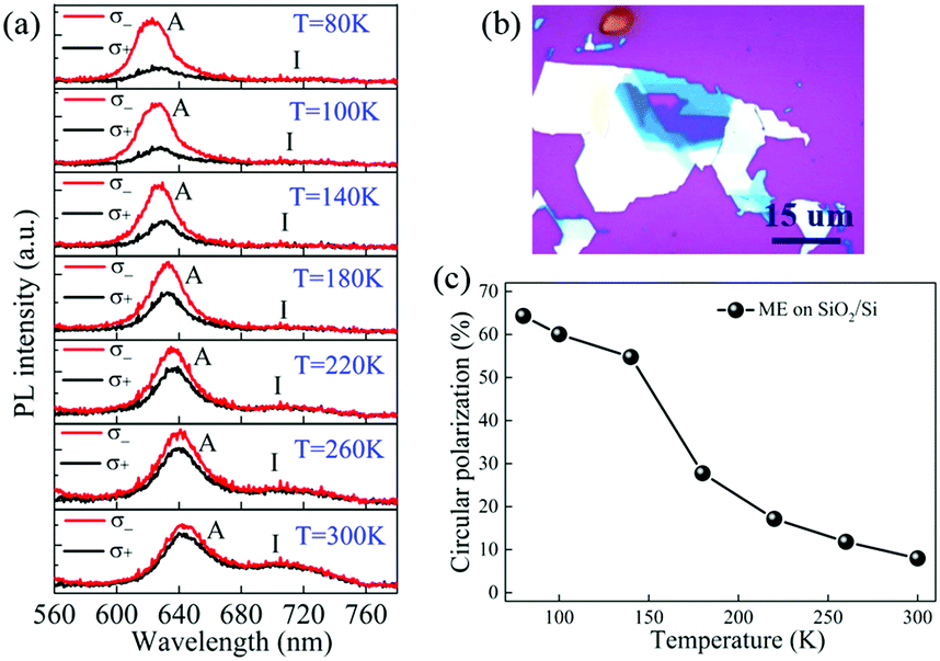 | ||
| Fig. 2 Circularly polarized behaviors of ME bilayer WS2 on a SiO2/Si substrate. (a) Circularly polarized components of PL spectra of as a function of temperature for ME bilayer WS2 on a SiO2/Si substrate. (b) Optical image of the ME bilayer WS2 sample. (c) Temperature dependence of circular polarization for ME bilayer WS2. The excitation light is left-circularly polarized in all the measurements. | ||
To probe whether the underlying substrate could influence the intervalley scattering, we then measured the circularly polarized behaviors of CVD-grown AA-stacked bilayer WS2 on the sapphire substrate (Fig. 3). As shown in Fig. 3a and b, CVD-grown AA-stacked bilayer WS2 on the sapphire substrate can be classified into two types based on their distinct valley polarization and light emission pattern. For the first kind of sample (marked as AA-1) with relatively large valley polarization (see also Fig. 3e), PL spectra contain obvious contribution of the I peak apart from the A exciton peak at high temperatures. In contrast, the I peak is much weaker for the other kind of bilayer sample (marked as AA-2) and its valley polarization is close to that of the CVD-grown AA-stacked bilayer WS2 on the SiO2/Si substrate. Therefore, it could be inferred that the valley polarization is associated with the intensity of the I peak. According to the calculated structural energy for WS2 bilayers with different stacking patterns, there are two possible high-symmetry AA stacking configurations, with the S atoms in the top layer placed above either the W atoms or the S atoms in the bottom layer.29 Due to steric effects, the interlayer distances are different for these two configurations,35 which may result in different interlayer coupling interactions and intensities of the I peak. The varying interlayer coupling strength in different CVD-grown bilayer WS2 samples will be further discussed later. In addition, the sharp and strong emission from the sapphire substrate appears at around 693 nm41 in all PL spectra and is circularly unpolarized over the whole temperature range. We also performed the temperature-dependent circularly polarized PL measurement on AB-stacked bilayer WS2 on a sapphire substrate (see Fig. S4 of the ESI†), but the signal-to-noise ratio is too low to resolve the valley behaviors due to the vanished interference effect, which fails to enhance the efficiency of light absorption and collection unlike a SiO2/Si substrate.42
 | ||
| Fig. 3 Circularly polarized behaviors of CVD-grown AA-stacked bilayer WS2 on a sapphire substrate. (a) Circularly polarized components of PL spectra as a function of temperature for AA-stacked bilayer WS2 with a relatively (a) strong and (b) weak I peak (marked as AA-1 and AA-2, respectively). (c) and (d) show optical images of the two bilayer WS2 samples corresponding to AA-1 and AA-2. (e) Temperature dependence of circular polarization for these two kinds of AA-stacked bilayer WS2 samples. The excitation light is left-circularly polarized in all the measurements. | ||
Finally, to obtain a comprehensive view of the correlation between the valley contrast and I peak, we compared the unpolarized PL spectra at room temperature and the corresponding valley behaviors of different types of bilayer WS2 samples in Fig. 4. It can be clearly seen that the valley polarization is indeed closely related to the intensity of the I peak in the bilayer WS2 samples (see Fig. 4a and b). More specifically, the bilayer WS2 samples with a relatively strong I peak have a larger valley contrast than those with relatively weak indirect bandgap emission. The link can be explained by phonons which play an important role in both the indirect transition and intervalley scattering process.14,35,43 The indirect transition in both AA- and AB-stacked bilayer WS2 occurs between Γ and Λ points29,36 with the assistance of Λ-point phonons for the momentum conservations. On the other hand, the intervalley scattering between K and K′ points requires the participation of a phonon with the corresponding wave vector difference,43 twice as large as that of the previous one which assists the indirect transition process.15 Therefore, the existence of a relatively strong I peak decreases the possibility of intervalley scattering by depleting phonons which may have participated in this process in pairs, leading to enhanced valley contrast. Among the three bilayer WS2 samples with a relatively weak indirect-gap emission peak, AA-stacked bilayer WS2 on the sapphire substrate has larger valley contrast than those on the SiO2/Si substrates at low temperature, which is attributed to the inheritance of the valley behaviors of monolayer WS2 on the two substrates (see Fig. S2 of the ESI†). To further confirm the relationship between valley polarization and the I peak, we explored the temperature dependence of valley polarization in five bilayer WS2 samples. Phonons are bosons and their number at equilibrium obeys Bose–Einstein statistics. As shown in Fig. 4b, for the bilayer samples which do not show a strong I peak, their circular polarization dependence on temperature can be well fitted by eqn (2), which is inversely proportional to the phonon population.
| ρ ∝ [exp(Ep/kBT) − 1] | (2) |
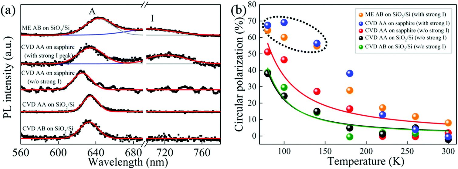 | ||
| Fig. 4 Dependence of circular polarization on the I peak. (a) PL spectra of different types of bilayer WS2 samples at 300 K. The PL features of sapphire were subtracted from the spectra of bilayer WS2 on a sapphire substrate for clarity. (b) Temperature dependence of circular polarization for different types of bilayer WS2 samples. | ||
| E p (meV) | ω p (cm−1) | Assignment | |
|---|---|---|---|
| CVD AA on SiO2 | 17.13 | 138.1 | ZA (Λ) |
| CVD AB on SiO2 | 19.15 | 154.5 | LA (Λ) |
| CVD AA on sapphire (without any strong I peak) | 12.55 | 101.2 | TA (Λ) |
From Fig. 4a, it should also be noticed that both the peak position and width vary for the PL spectra of different types of bilayer WS2 samples. The redshift of the I peak in AA-stacked bilayer WS2 compared with ME bilayer WS2 is due to the lower energy of indirect transition for AA-stacked bilayer WS2 according to theoretical calculation.29 For the A exciton peak, the relative shift is attributed to the combined effect of interlayer coupling and local strain induced by the sample–substrate interactions. A comparison of PL spectra for the samples on the same substrate (i.e. ME versus CVD-grown AA/AB-stacked bilayer WS2 on SiO2/Si and CVD-grown AA-1 versus AA-2 bilayer WS2 on sapphire) demonstrates that the energies of the A exciton peak for bilayer WS2 with a relatively stronger I peak generally redshift compared to those with a weak indirect-gap emission peak. The weak I peak manifests relatively weakened interlayer coupling and therefore the peak positions of the A excitons for bilayer WS2 with a relatively weak indirect-gap emission peak exhibit blueshifts towards those of monolayer WS2 at higher energies.39,46 To further confirm that the shift is indeed caused by interlayer coupling, we compared the frequency differences of the E12g(Γ) and A1g(Γ) modes in different types of bilayer WS2 samples on SiO2/Si substrates, which are indicative of the interlayer coupling strength.35,47 As shown in Fig. S5 of the ESI,† the separation of the E12g(Γ) and A1g(Γ) modes is larger in ME bilayer WS2 than those of the CVD-grown bilayer counterparts, which demonstrates stronger interlayer coupling in the ME sample and provides support for our explanation of the exciton shift for samples on the same substrate from the viewpoint of interlayer coupling. The distinct strength of interlayer coupling is attributed to the change in interlayer distances in the different types of bilayer WS2 samples since van der Waals interaction is negatively related to the interlayer distances.35,48 In contrast to the ME bilayer WS2 sample, the uncontrollable variation of the interlayer distance in different types of CVD-grown bilayer samples could lead to varying interlayer coupling strength.35 Future work will investigate the underlying cause of the varying interlayer coupling strength in different CVD-grown bilayer WS2 samples, even on the same sapphire substrate. Moreover, for the same kind of bilayer WS2 sample (i.e. bilayer WS2 with either a strong or a weak I peak) on different substrates, the relative shift of the A exciton peak might be due to the local strain induced by the sample–substrate interactions during the exfoliation or growth process, which has been commonly observed in atomically thin layered materials.49–54 The lower surface roughness of sapphire compared to SiO249 makes the conformally adhered bilayer WS2 on it subject to smaller tensile strain and leads to higher energies of the exciton peak for bilayer WS2 on the sapphire substrate.32,55 This is consistent with our observation of the exciton redshift in ME (CVD-grown AA/AB-stacked) bilayer WS2 on the SiO2/Si substrate relative to the CVD-grown AA-2 (AA-1) counterpart on the sapphire substrate. Furthermore, it is known that the exciton–phonon interactions broaden the linewidths of excitons.56 For the variation of exciton width as shown in Fig. 4a, the ME and CVD-grown AA-1 bilayer WS2 have broader A exciton peaks than the other bilayer samples, which reflects the stronger exciton–phonon interaction in these two types of samples.
Experimental
Monolayer and bilayer WS2 samples were fabricated by mechanical exfoliation and grown by the CVD method, followed by temperature-dependent circularly polarized PL measurements.Sample preparation
CVD monolayer and bilayer WS2 samples were grown on 300 nm SiO2/Si and sapphire substrates by a previously reported technique.57 Compared with the experimental process to grow monolayer WS2, the growth time at 750 °C was increased for bilayer WS2, which could make vertical layer-by-layer growth more preferable.35 Exfoliated WS2 flakes used in this work were obtained by mechanical cleavage of a bulk 2H-WS2 crystal (2D Semiconductors, CAS #12138-09-9, USA) and then transferred onto 300 nm SiO2/Si substrates. Monolayer and bilayer WS2 flakes were selected using an optical microscope (Olympus BX 51), followed by confirmation through PL/Raman spectroscopy.Optical characterization
The PL measurements were performed with a WITec CRM200 confocal Raman system under a 532 nm excitation laser with a 150 lines per mm grating. To achieve polarization-resolved PL measurements, the linearly polarized light was first transformed into left-circularly polarized light by passing through an achromatic quarter-wave plate (WPQ10M-532, Thorlabs) and then shone on the sample. Next, the emitted backscattering beam comprising both left- and right-circularly light got through the same quarter-wave plate and was separated into two perpendicularly polarized beams, which could be separately detected by rotating the linear polarizer located on top of the edge filter. The accuracy of the circular polarization degree for our setup was no less than 94.0%. The linear polarizer was rotated cautiously to avoid any perturbation effect on the collimation of the whole system throughout the experiment. After both the left- and right-circularly polarized components of PL spectra were measured, the linear polarizer was rotated back to the original position to confirm that the measured spectrum was fully reproducible. To achieve a fair comparison by ruling out the hysteresis effect, all temperature-dependent PL measurements were performed from room temperature down to 80 K. The cooling of the samples was realized using a temperature controlled stage HFS600E (Linkam Scientific Instruments). At each temperature, at least two different points were tested to confirm that the observed trend of the spectral change was typical. A long-working distance 50× objective lens was used in all the PL measurements with a numerical aperture of 0.55. Raman measurements were carried out by the same WITec system under a 532 nm excitation laser with a 1800 grooves per mm grating at room temperature. The laser spot was evaluated to be around 1 μm. The laser power at the sample surface was maintained with great care to avoid laser-induced damage and kept unchanged during the temperature-dependent measurement.Conclusions
In summary, we investigated temperature-dependent valley polarization in various AA- and AB-stacked bilayer WS2 samples and experimentally demonstrated the correlation between the intensity of the indirect bandgap emission and valley polarization. We showed that acoustic phonons play a leading role in the valley polarization of bilayer WS2 and the depletion of such phonons in the indirect optical transition process could contribute to the exceptionally robust valley polarization. Our results shed light on the critical role of electron–phonon coupling in the intervalley scattering process in bilayer WS2 and lay a foundation for developing valleytronic applications exploiting the strong electron–phonon interaction in 2D TMDs. Our findings provide new insights into the realization of more robust valley polarization in broader 2D systems by manipulating the indirect optical transition and intervalley scattering.Conflicts of interest
There are no conflicts to declare.Acknowledgements
This work was supported by the National Natural Science Foundation of China (No. 61774040 and 11774170), Ministry of Education (MOE) Tier 1 RG199/17, the National Young 1000 Talent Plan of China, the Shanghai Municipal Natural Science Foundation (No. 16ZR1402500), the Opening project of the State Key Laboratory of Functional Materials for Informatics, the Shanghai Institute of Microsystem and Information Technology, the Chinese Academy of Sciences, the China Postdoctoral Science Foundation (Grant 2018M631829), the dedicated grant for methanol conversion from DICP, the Six Talent Peaks project in Jiangsu Province under grant number 51235079, and the 100 Foreign Talents Project in Jiangsu Province under grant number 51235228.References
- S. Jo, N. Ubrig, H. Berger, A. B. Kuzmenko and A. F. Morpurgo, Nano Lett., 2014, 14, 2019–2025 CrossRef CAS PubMed.
- T. Georgiou, R. Jalil, B. D. Belle, L. Britnell, R. V. Gorbachev, S. V. Morozov, Y.-J. Kim, A. Gholinia, S. J. Haigh, O. Makarovsky, L. Eaves, L. A. Ponomarenko, A. K. Geim, K. S. Novoselov and A. Mishchenko, Nat. Nanotechnol., 2013, 8, 100–103 CrossRef CAS PubMed.
- R. C. Cooper, C. Lee, C. A. Marianetti, X. Wei, J. Hone and J. W. Kysar, Phys. Rev. B: Condens. Matter Mater. Phys., 2013, 87, 035423 CrossRef.
- Y. Zhang, J. Ye, Y. Matsuhashi and Y. Iwasa, Nano Lett., 2012, 12, 1136–1140 CrossRef CAS PubMed.
- C. Cong, J. Shang, Y. Wang and T. Yu, Adv. Opt. Mater., 2018, 6, 1700767 CrossRef.
- G. B. Liu, D. Xiao, Y. Yao, X. Xu and W. Yao, Chem. Soc. Rev., 2015, 44, 2643–2663 RSC.
- C. Qin, Y. Gao, Z. Qiao, L. Xiao and S. Jia, Adv. Opt. Mater., 2016, 4, 1429–1456 CrossRef CAS.
- H. Kwon, K. Lee, J. Heo, Y. Oh, H. Lee, S. Appalakondaiah, W. Ko, H. W. Kim, J. W. Jung, H. Suh, H. Min, I. Jeon, E. Hwang and S. Hwang, Adv. Mater., 2017, 29, 1702931 CrossRef PubMed.
- F. Barati, M. Grossnickle, S. Su, R. K. Lake, V. Aji and N. M. Gabor, Nat. Nanotechnol., 2017, 12, 1134–1139 CrossRef CAS PubMed.
- H. Zeng and X. Cui, Chem. Soc. Rev., 2015, 44, 2629–2642 RSC.
- Y. Wan, J. Xiao, J. Li, X. Fang, K. Zhang, L. Fu, P. Li, Z. Song, H. Zhang, Y. Wang, M. Zhao, J. Lu, N. Tang, G. Ran, X. Zhang, Y. Ye and L. Dai, Adv. Mater., 2018, 30, 1703888 CrossRef PubMed.
- X. Chen, T. Yan, B. Zhu, S. Yang and X. Cui, ACS Nano, 2017, 11, 1581–1587 CrossRef CAS PubMed.
- C. F. Hirjibehedin, Nat. Phys., 2013, 9, 756–757 Search PubMed.
- B. Zhu, H. Zeng, J. Dai, Z. Gong and X. Cui, Proc. Natl. Acad. Sci. U. S. A., 2014, 111, 11606–11611 CrossRef CAS PubMed.
- K. F. Mak, K. He, J. Shan and T. F. Heinz, Nat. Nanotechnol., 2012, 7, 494–498 CrossRef CAS PubMed.
- A. M. Jones, H. Yu, N. J. Ghimire, S. Wu, G. Aivazian, J. S. Ross, B. Zhao, J. Yan, D. G. Mandrus, D. Xiao, W. Yao and X. Xu, Nat. Nanotechnol., 2013, 8, 634–638 CrossRef CAS PubMed.
- R. Suzuki, M. Sakano, Y. J. Zhang, R. Akashi, D. Morikawa, A. Harasawa, K. Yaji, K. Kuroda, K. Miyamoto, T. Okuda, K. Ishizaka, R. Arita and Y. Iwasa, Nat. Nanotechnol., 2014, 9, 611–617 CrossRef CAS PubMed.
- W. Yao, D. Xiao and Q. Niu, Phys. Rev. B: Condens. Matter Mater. Phys., 2008, 77, 235406 CrossRef.
- H. Yu, X. Cui, X. Xu and W. Yao, Natl. Sci. Rev., 2015, 2, 57–70 CrossRef CAS.
- D. Xiao, G. B. Liu, W. Feng, X. Xu and W. Yao, Phys. Rev. Lett., 2012, 108, 196802 CrossRef PubMed.
- D. Lagarde, L. Bouet, X. Marie, C. R. Zhu, B. L. Liu, T. Amand, P. H. Tan and B. Urbaszek, Phys. Rev. Lett., 2014, 112, 047401 CrossRef CAS PubMed.
- G. Kioseoglou, A. T. Hanbicki, M. Currie, A. L. Friedman and B. T. Jonker, Sci. Rep., 2016, 6, 25041 CrossRef CAS PubMed.
- S. Wu, J. S. Ross, G.-B. Liu, G. Aivazian, A. Jones, Z. Fei, W. Zhu, D. Xiao, W. Yao, D. Cobden and X. Xu, Nat. Phys., 2013, 9, 149–153 Search PubMed.
- T. Jiang, H. Liu, D. Huang, S. Zhang, Y. Li, X. Gong, Y. R. Shen, W. T. Liu and S. Wu, Nat. Nanotechnol., 2014, 9, 825–829 CrossRef CAS PubMed.
- Z. Gong, G. B. Liu, H. Yu, D. Xiao, X. Cui, X. Xu and W. Yao, Nat. Commun., 2013, 4, 2053 CrossRef PubMed.
- A. M. Jones, H. Yu, J. S. Ross, P. Klement, N. J. Ghimire, J. Yan, D. G. Mandrus, W. Yao and X. Xu, Nat. Phys., 2014, 10, 130–134 Search PubMed.
- P. K. Nayak, F. C. Lin, C. H. Yeh, J. S. Huang and P. W. Chiu, Nanoscale, 2016, 8, 6035–6042 RSC.
- Q. Liu, X. Zhang and A. Zunger, Phys. Rev. Lett., 2015, 114, 087402 CrossRef PubMed.
- J. He, K. Hummer and C. Franchini, Phys. Rev. B: Condens. Matter Mater. Phys., 2014, 89, 075409 CrossRef.
- S. Zheng, L. Sun, X. Zhou, F. Liu, Z. Liu, Z. Shen and H. J. Fan, Adv. Opt. Mater., 2015, 3, 1600–1605 CrossRef CAS.
- G. Plechinger, P. Nagler, J. Kraus, N. Paradiso, C. Strunk, C. Schüller and T. Korn, Phys. Status Solidi RRL, 2015, 9, 457–461 CrossRef CAS.
- Y. Wang, C. Cong, W. Yang, J. Shang, N. Peimyoo, Y. Chen, J. Kang, J. Wang, W. Huang and T. Yu, Nano Res., 2015, 8, 2562–2572 CrossRef CAS.
- J. S. Ross, S. Wu, H. Yu, N. J. Ghimire, A. M. Jones, G. Aivazian, J. Yan, D. G. Mandrus, D. Xiao, W. Yao and X. Xu, Nat. Commun., 2013, 4, 1474 CrossRef PubMed.
- X. X. Zhang, Y. You, S. Y. Zhao and T. F. Heinz, Phys. Rev. Lett., 2015, 115, 257403 CrossRef PubMed.
- K. Liu, L. Zhang, T. Cao, C. Jin, D. Qiu, Q. Zhou, A. Zettl, P. Yang, S. G. Louie and F. Wang, Nat. Commun., 2014, 5, 4966 CrossRef CAS PubMed.
- W. Zhao, R. M. Ribeiro, M. Toh, A. Carvalho, C. Kloc, A. H. Castro Neto and G. Eda, Nano Lett., 2013, 13, 5627–5634 CrossRef CAS PubMed.
- H. Zeng, G. B. Liu, J. Dai, Y. Yan, B. Zhu, R. He, L. Xie, S. Xu, X. Chen, W. Yao and X. Cui, Sci. Rep., 2013, 3, 1608 CrossRef PubMed.
- R. Akashi, M. Ochi, S. Bordács, R. Suzuki, Y. Tokura, Y. Iwasa and R. Arita, Phys. Rev. A: At., Mol., Opt. Phys., 2015, 4, 014002 Search PubMed.
- W. Zhao, Z. Ghorannevis, L. Chu, M. Toh, C. Kloc, P.-H. Tan and G. Eda, ACS Nano, 2012, 7, 791–797 CrossRef PubMed.
- S. W. Han, H. Kwon, S. K. Kim, S. Ryu, W. S. Yun, D. H. Kim, J. H. Hwang, J. S. Kang, J. Baik, H. J. Shin and S. C. Hong, Phys. Rev. B: Condens. Matter Mater. Phys., 2011, 84, 045409 CrossRef.
- V. Kudryashov, S. Mamakin and A. Yunovich, Tech. Phys. Lett., 1999, 25, 536–537 CrossRef CAS.
- M. Buscema, G. A. Steele, H. S. J. van der Zant and A. Castellanos-Gomez, Nano Res., 2015, 7, 561–571 CrossRef.
- H. Zeng, J. Dai, W. Yao, D. Xiao and X. Cui, Nat. Nanotechnol., 2012, 7, 490–493 CrossRef CAS PubMed.
- A. Molina-Sánchez and L. Wirtz, Phys. Rev. B: Condens. Matter Mater. Phys., 2011, 84, 155413 CrossRef.
- B. R. Carvalho, Y. Wang, S. Mignuzzi, D. Roy, M. Terrones, C. Fantini, V. H. Crespi, L. M. Malard and M. A. Pimenta, Nat. Commun., 2017, 8, 14670 CrossRef PubMed.
- H. R. Gutierrez, N. Perea-Lopez, A. L. Elias, A. Berkdemir, B. Wang, R. Lv, F. Lopez-Urias, V. H. Crespi, H. Terrones and M. Terrones, Nano Lett., 2013, 13, 3447–3454 CrossRef CAS PubMed.
- A. M. van der Zande, J. Kunstmann, A. Chernikov, D. A. Chenet, Y. You, X. Zhang, P. Y. Huang, T. C. Berkelbach, L. Wang, F. Zhang, M. S. Hybertsen, D. A. Muller, D. R. Reichman, T. F. Heinz and J. C. Hone, Nano Lett., 2014, 14, 3869–3875 CrossRef CAS PubMed.
- S. Huang, X. Ling, L. Liang, J. Kong, H. Terrones, V. Meunier and M. S. Dresselhaus, Nano Lett., 2014, 14, 5500–5508 CrossRef CAS PubMed.
- H. Sahin, S. Tongay, S. Horzum, W. Fan, J. Zhou, J. Li, J. Wu and F. M. Peeters, Phys. Rev. B: Condens. Matter Mater. Phys., 2013, 87, 165409 CrossRef.
- B. G. Shin, G. H. Han, S. J. Yun, H. M. Oh, J. J. Bae, Y. J. Song, C. Y. Park and Y. H. Lee, Adv. Mater., 2016, 28, 9378–9384 CrossRef CAS PubMed.
- Z. Liu, M. Amani, S. Najmaei, Q. Xu, X. Zou, W. Zhou, T. Yu, C. Qiu, A. G. Birdwell, F. J. Crowne, R. Vajtai, B. I. Yakobson, Z. Xia, M. Dubey, P. M. Ajayan and J. Lou, Nat. Commun., 2014, 5, 5246 CrossRef PubMed.
- Z.-Q. Xu, Y. Zhang, S. Lin, C. Zheng, Y. L. Zhong, X. Xia, Z. Li, P. J. Sophia, M. S. Fuhrer and Y.-B. Cheng, ACS Nano, 2015, 9, 6178–6187 CrossRef CAS PubMed.
- R. V. Gorbachev, I. Riaz, R. R. Nair, R. Jalil, L. Britnell, B. D. Belle, E. W. Hill, K. S. Novoselov, K. Watanabe, T. Taniguchi, A. K. Geim and P. Blake, Small, 2011, 7, 465–468 CrossRef CAS PubMed.
- W. G. Cullen, M. Yamamoto, K. M. Burson, J. H. Chen, C. Jang, L. Li, M. S. Fuhrer and E. D. Williams, Phys. Rev. Lett., 2010, 105, 215504 CrossRef CAS PubMed.
- A. Kumar and P. K. Ahluwalia, Modell. Simul. Mater. Sci. Eng., 2013, 21, 065015 CrossRef.
- S. Rudin, T. Reinecke and B. Segall, Phys. Rev. B: Condens. Matter Mater. Phys., 1990, 42, 11218–11231 CrossRef CAS.
- C. Cong, J. Shang, X. Wu, B. Cao, N. Peimyoo, C. Qiu, L. Sun and T. Yu, Adv. Opt. Mater., 2014, 2, 131–136 CrossRef.
Footnote |
| † Electronic supplementary information (ESI) available. See DOI: 10.1039/c8nh00306h |
| This journal is © The Royal Society of Chemistry 2019 |