
Erasable memory properties of spectral selectivity modulated by temperature and bias in an individual CdS nanobelt-based photodetector
Tao
Tong
a,
Shujuan
Wang
a,
Jie
Zhao
b,
Baochang
Cheng
 *ab,
Yanhe
Xiao
b and
Shuijin
Lei
b
*ab,
Yanhe
Xiao
b and
Shuijin
Lei
b
aNanoscale Science and Technology Laboratory, Institute for Advanced Study, Nanchang University, Jiangxi 330031, P. R. China. E-mail: bcheng@vip.sina.com
bSchool of Materials Science and Engineering, Nanchang University, Jiangxi 330031, P. R. China
First published on 31st August 2018
Abstract
Single CdS nanobelt-based photodetectors are strongly dependent on bias and temperature. They not only show a strong photoresponse to close bandgap energy light with ultrahigh responsivity of approximately 107 A W−1, large photo-to-dark current ratio of 104, photoconductive gain of 107, and fast response and recovery speed at a large bias of 20 V, but can also show a weak photoresponse to above- and below-bandgap energy light. Moreover, their spectral response range can show tunable selectivity to above- and below-bandgap light, which can be accurately controlled by temperature and bias. More importantly, the modulated spectral response characteristics show excellent memory behaviour after reversible writing and erasing by using temperature and bias. In nanostructures, abundant surface states and stacking fault-related traps play a vital role in the ultrahigh photoresponse to bandgap light and the erasable memory effect on spectral response range selectivity. Given the erasable memory of the spectral response selectivity with excellent photoconduction performance, the CdS NBs possess important applications in new-generation photodetection and photomemory devices.
Conceptual insightsClassical photodetectors generally only show a strong photoresponse to above-bandgap light. In CdS nanostructures, however, the presence of surface states related to lattice periodicity breaking and traps associated with stacking faults change the conventional photoconductivity. The appropriate temperature can induce traps to empty, while large bias can induce traps to fill, which in turn increases and decreases the width of the surface barrier, respectively. Therefore, the photoresponse region can transform from a depletion region with emptied traps into an interior region with filled traps. Moreover, the filled and emptied traps can be maintained at low operation bias and room temperature, manifesting a reversible writing and erasing memory effect. |
1. Introduction
As the foundation of modern information and new energy technologies, nanostructure semiconductors have captured extensive attention, and their development and application have brought great convenience to people. In particular, their development and progress in computers, artificial intelligence, communications, aerospace and weapons have played a vital role in national security and the national economy. In recent decades, therefore, the construction and integration of nanodevices based on nanosemiconductors have developed rapidly.1–5 One-dimensional (1D) nanosemiconductors in particular have many advantages that are superior to other materials.6–14 On their surfaces, a large number of dangling bonds can be formed owing to the damage of the lattice periodicity, and thus surface states are generated on their surfaces.15,16 For surface traps, moreover, the filling and emptying of charges can be controlled by external stimuli, such as acoustic, optical, electrical, magnetic and heating, thereby obtaining unique properties that are different from those of bulk materials.17–19 When constructing a two-terminal nanodevice, in addition, a large number of surface states will form two back-to-back connected diodes at the semiconductor material and two metal electrode interfaces, and moreover the barrier of surface state-related diodes can also be adjusted at both ends, which will have a great impact on the performance of nanodevices.20–23 Therefore, the modulation of the surface states of nanosemiconductors has become a hot issue in the field of nanodevices.As one of the most studied metal chalcogenides, cadmium sulfide (CdS) is a direct bandgap semiconductor with about 2.42 eV, which has excellent physicochemical properties such as relatively low work function, large refraction index, high sensitivity, fast response, excellent thermal, and chemical stability.24–26 Therefore, it is a promising material for electronic and optoelectronic applications, such as field-effect transistors.27,28 photodetectors.29–37 solar cells,38–41 switches,42–44 and logic circuits.45,46 The current research on CdS-based photodetectors is mainly focused on the ultraviolet (UV)-visible (VIS) light range owing to the proper bandgap width.47–49 However, it is precisely the bandgap width of CdS that limits its response to VIS-near infrared (NIR) light, which will greatly limit the application of these photodetectors in the longer wavelength range. Therefore, how to adjust the spectral response range of CdS is overwhelmingly important for the fabrication of high-performance photodetectors. Especially for photodetectors, if their spectral response range selectivity can effectively be memorized, it will extend their application in photomemories.
In this paper, CdS nanobelts (NBs) were synthesized by a thermal evaporation method,50–52 and then an individual NB-based metal–semiconductor–metal (MSM) two-terminal device was fabricated with two similar silver electrodes.11 By systematically exploring the photoresponse characteristics under different bias voltages, illumination intensities and temperatures, it was found that CdS NB not only can show ultrahigh photoresponse to close bandgap light at a relatively large bias, but also can show temperature and bias dependence of spectral response range selectivity. More importantly, the modulated spectral response characteristics can be memorized at low operation bias and room temperature after reversibly writing and erasing by relatively high temperature and bias. This will enable CdS NBs to be fabricated as a high-performance temperature- and bias-controlled erasable photomemory with excellent selection and memory performance of spectral response.
2. Experimental
2.1. Synthesis of CdS NBs and fabrication of NB-based photodetector
The CdS NBs employed in this work were synthesized by a thermal evaporation method. A horizontal alumina tube was installed inside a tubular furnace. High purity CdS (99.99%) powder was placed at the center of the alumina tube. Before heating, the tube was held in a constant flow of mixed 40 ml min−1 gas (90% N2 + 10% H2) for 30 min to ensure the elimination of O2. The furnace was heated to 1200 °C with a flow rate of 20 ml min−1 and then held for 60 min. After leaving to cool naturally, CdS NBs were obtained on the inner wall of the alumina tube.For the fabrication of an individual NB-based photodetector, a relatively long single CdS NB was transferred on to a flexible Kapton substrate and then the device was fabricated by the contact of semi-dried sliver paste with two ends of a CdS NB. Finally, copper wires were bonded to the silver electrodes for measurement.
2.2. Characterization of materials and measurements of devices
The morphology and microstructure of the as-synthesized products were analyzed by means of X-ray diffraction (XRD; RIGAKU D/max-3b), field emission environmental scanning electron microscopy (FESEM, FEI Quanta 200F), and high-resolution transmission electron microscopy (HRTEM, JEOL JEM-2010), respectively. For photodetection experiments, the continuous and monochromatic wavelength-light source was provided by a fluorescence spectrophotometer (Hitachi F-4600) with a 150 W Xe lamp. For micro-optical detection, the incident light source was provided by a microscope objective. Temperature-controlled detection experiments were performed using an intelligent temperature control platform. For asymmetrical temperature measurement, the temperature was provided by an intelligent temperature control electric iron. For PL mapping observation, a single NB-based device was fabricated on a thin quartz substrate and then observed by laser scanning confocal microscopy (LSCM, Zeiss LSM710) using a diode laser with 405 nm wavelength as the excitation light source. The light emitted from the NB was collected by an objective lens. The detection system operates efficiently in the spectral range from 420 to 720 nm. The electrical measurement was conducted using a synthesized function generator (Stanford Research System Model DS345) and a low-noise current preamplifier (Stanford Research System Model SR570).3. Results and discussion
3.1. Characterization of materials
The XRD pattern of the as-synthesized product is shown in Fig. 1a. It can well be fitted with JCPDS card 41-1049. Moreover, no characteristic peaks of other crystals were detected, indicating that the product is composed of hexagonal phase CdS. The component was analyzed by energy-dispersive X-ray spectroscopy (EDS), as illustrated in Fig. 1b, and the results manifest that the product is only composed of Cd and S without the introduction of other elements. The microstructure and morphology of the product were further measured by FESEM and HRTEM, as shown in Fig. 1c–e. They clearly demonstrate that the product is smooth ribbon-like 1D nanostructures with “Z”-type shape, and their length is in the range from tens to hundreds of microns. Then, the lattice fringe image of the obtained product and the corresponding selected area electron diffraction (SAED), as illustrated in Fig. 1f, prove that CdS is grown along the [0001] direction, and moreover quantities of stacking faults exist in the {0001} planes. | ||
| Fig. 1 Structural characterization of as-synthesized CdS NBs. (a) XRD pattern, revealing the formation of hexagonal wurtzite CdS (JCPDS: 41-1049); (b) EDS spectrum, indicating that the sample is composed of Cd and S; (c) and (d) FESEM images, showing “Z” type bending shape; (e) bright-field TEM image; (f) HRTEM image, and the inset corresponds to its SAED pattern, revealing representative stacking fault features in NB growing along [0001]. | ||
3.2. Realization of green photodetector with high performance in a single NB-based device
Fig. 2 illustrates systematically the possibility of whether a device based on a single CdS NB can be fabricated into a high-performance photodetector with controllable properties modulated by external bias and illumination intensity. Fig. 2a and b show the spectral response characteristics of the device at different bias voltages and incident light intensities, respectively. It can clearly be seen that the spectral response of the device is intensively correlated with bias voltage and light intensity. At relatively low operation bias and illumination intensity, the device hardly shows photoresponse to light of wavelength ranging from UV to NIR. With the increase of applied bias voltage and incident light intensity, however, the device displays a strong photoresponse to green light with a wavelength of about 510 nm, which is consistent with the bandgap energy of CdS. Especially for higher illumination intensity, as seen from Fig. 2b, the device shows a stronger photoresponse to the green light with narrow width. In addition, it shows a certain degree of response to the light from UV and NIR as well; however, the response to the light with wavelength ranging from 200 to 550 nm is relatively strong. To further verify the photoresponse characteristics, the device was irradiated under different wavelengths of 350, 510, 670, and 830 nm at fixed illumination intensity of 140 μW cm−2 and bias of 1 V, as shown in Fig. 2c and d. It can clearly be seen that the device shows a response to all these lights ranging from UV to NIR, and the on/off ratios can reach 102, 103, 5, 5 for light with wavelength of 350, 510, 670, and 830 nm, respectively. Moreover, their response and recovery time is lower than 0.1 s. In addition, they also show excellent stability and repeatability. At a fixed bias of 1 V, the photoresponse of the device was also measured using a 510 nm green light with different irradiation intensities of 4, 10, 35, and 140 μW cm−2, as illustrated in Fig. 2e and f, and their on/off ratios can all reach 103. To further explore the influence of bias, the photoresponse was also measured using a 510 nm green light with different intensities at 20 V bias, as shown in Fig. 2g and h, and their on/off ratio can reach 104. As seen from Fig. 2g, the I–V curves are also nonlinear under illumination, and moreover their currents give a trend of saturation with an increase in bias at much higher illumination intensity.53,54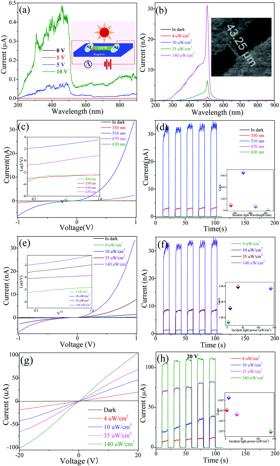 | ||
| Fig. 2 Under different illumination intensities and bias voltages, the photoresponse characteristics of an individual CdS NB-based photodetector at room temperature. (a) Under different fixed biases of 0, 1, 5 and 10 V, the spectral response vs. wavelengths at an illumination intensity of about 10 μW cm−2. The inset in (a) represents a schematic illustration of the device for photoconduction measurement. (b) Under different illumination intensities of 0, 4, 10, 35 and 140 μW cm−2, the spectral response vs. wavelengths at a fixed bias of 1 V. The inset in (b) corresponds to an FESEM image of a two-terminal photodetector. (c) and (d) Under light illumination with different wavelengths of 350, 510, 670 and 830 nm, I–V characteristics and on/off response of photodetector at a fixed bias voltage of 1 V. The insets in (c) and (d) correspond to the plots of P–F mechanism fitting [sqrt(V) − ln(I/V)] for the forward-biased part in (c) and photoconductive gain, respectively. (e) and (f) Under 510 nm green light irradiation with different intensities, I–V characteristics and on/off response of photodetector at 1 V bias. The insets in (e) and (f) correspond to the plots of the P–F mechanism fitting for the forward-biased part in (e) and photoconductive gain, respectively. (g) and (h) Under 510 nm green light irradiation with different intensities, I–V characteristics and on/off response of photodetector at 20 V bias. The inset in (h) corresponds to the plot of photoconductive gain. | ||
The photoresponse behaviour of the detectors was also characterized by measuring the current at different fixed bias voltages as a function of time when the device was periodically exposed to light with different wavelengths, as shown in Fig. 2d, f and g. It can clearly be observed that the photocurrent is strongly dependent on the applied bias voltage, and the wavelength and power density of incident light. The external quantum efficiency (photoconductive gain G), defined as the number of electrons collected by electrodes due to the excitation by one incident photon, can be calculated by the follow equation:16,48,55,56
| G = (hν/e)(ΔI/P) | (1) |
As seen from Fig. 2c and e, I–V curves are nonlinear, and moreover they are not completely symmetrical at forward and reverse bias voltages. However, they can all be fitted well by the Poole–Frenkel (P–F) emission mechanism, and a linear increase relation of ln(I/V) versus V1/2 can be obtained, indicating that the conduction mechanism in the photodetectors mainly arises from the bulk trap-related P–F hopping rather than the NB–electrode interface barrier variation in a low voltage range of 0–1 V. The P–F emission refers to electric-field-enhanced thermal emission from a trapped state into a continuum of electronic state, which is usually, but not necessarily, the conduction band in an insulator. If this mechanism is assumed, the current through the photodetector can be calculated by:58
I = CV![[thin space (1/6-em)]](https://www.rsc.org/images/entities/char_2009.gif) exp(−q(ϕ − (qV/πε0εr)1/2)/kT) exp(−q(ϕ − (qV/πε0εr)1/2)/kT) | (2) |
Compared with the low measurement bias, as seen from Fig. 2h and g, the photodetector not only shows a much larger photoconductive gain at a larger operation bias, but also its I–V curves show a saturation tendency with bias under illumination. For the two-terminal devices, two back-to-back connected diodes with series resistance can be formed. At a larger operation bias, traps can be filled well, and the width of the surface barrier is extremely thin. The influence of traps on the electrical transport can be neglected. Therefore, the interface barrier will play a crucial role compared with trap hopping. For the thin surface barriers with trap filling, the thermionic emission mechanism of two back-to-back diodes is predominant under illumination, and correspondingly I–V curves show saturation tendency with increasing forward and reverse bias.
3.3. Adjustment and memory of spectral response range
For the high performance of single CdS NB-based photodetectors with wide spectral response, if their spectral response range can be selectively adjusted and accurately controlled, they will can be applied in wider areas. All the above measurements were conducted at room temperature. Next, we will further explore the relationship between photoresponse and temperature for a single CdS NB-based detector. Fig. 3a shows the temperature dependence of photocurrent variation under illumination of 510 nm green light at 0.5 V fixed bias. The photocurrent first increases with temperature. It reaches a maximum at around 100 °C, and afterwards decreases with further increasing temperature, demonstrating a negative differential resistance behaviour. When the temperature is higher than about 200 °C, the current increases again with temperature. In the temperature range from 25 to 300 °C, the current of the device shows an obvious “S” shape under illumination of 510 nm green light. Generally speaking,48 the conduction is thought to arise from impurity ionization at the initial rise stage of “AB”. In the fall stage of “BC”, it originates from a lattice vibration scattering due to complete ionization of impurities. The rise again in stage “CD” arises from an intrinsic excitation of CdS. Meanwhile, the I–V characteristics were also measured at different temperatures under illumination with 510 nm green light at 0.5 V bias voltage, as illustrated in Fig. 3b. Similarly, the current increases with temperature, then decreases, and finally increases again. From the I–V curves fitted by P–F mechanism, it can be seen that the slope of the curves is almost similar, except for those measured at 100 and 150 °C. The emptying of traps can give rise to the decrease of the dynamic dielectric constant εr, and accordingly the slope increases at 100 and 150 °C.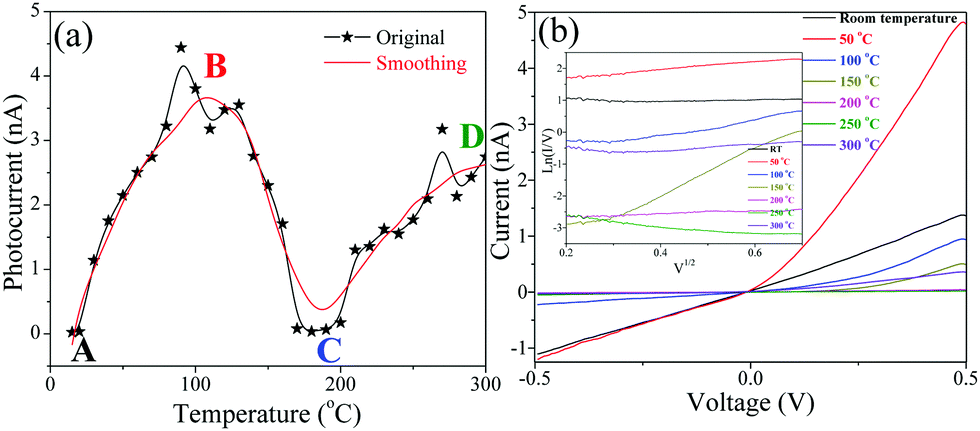 | ||
| Fig. 3 At different temperatures, the current response characteristics of the photodetector under illumination with 510 nm green light. (a) At a fixed bias voltage of 0.5 V, the relationship between photocurrent and temperature ranging from 25 to 300 °C; (b) under different temperatures, I–V characteristics measured at 0.5 V bias. | ||
The spectral response range of a single CdS NB-based photodetector was measured at different temperatures at a fixed bias of 0.5 V, as illustrated in Fig. 4. As can be seen from the figures, an interesting phenomenon was found. That is, the spectral response range of the detector can show an apparent selectivity in temperature ranging from 25 to 250 °C. At room temperature, the photodetector shows a very strong response to above-bandgap light in the wavelength range from UV to green, and furthermore it can also show a weak response to light with wavelengths longer than 500 nm. With the increase of temperature, the response to UV light decreases, and nevertheless it becomes more obvious for below-bandgap light. When the temperature reaches about 150 °C, the device only shows a response to light ranging from roughly 500 to 800 nm, centering at 560 nm. However, the response to light with wavelength ranging from UV to green increases again when the temperature is higher than about 200 °C. When the temperature reaches about 250 °C, the photodetector shows a stronger response to above-bandgap light again, and in contrast the response to below-bandgap light becomes relatively weak.
 | ||
| Fig. 4 At different temperatures, the spectral response of the detector vs. wavelengths under continuous (left) and periodic chopping (right) light source. (a) and (b) Room temperature of 25 °C; (c) and (d) 50 °C; (e) and (f) 100 °C; (g) and (h) 150 °C; (i) and (j) 200 °C; (k) and (l) 250 °C. | ||
For spectral response range, the photodetector shows strong selectivity with temperature. At temperatures lower than 50 °C and higher than 250 °C, the device shows an excellent response to above-bandgap light with wavelength shorter than about 510 nm. Although it also shows a response to light with wavelength longer than 500 nm, it is too weak to consider. In contrast, the device is more sensitive to below-bandgap light with wavelength longer than 500 nm at temperatures ranging from 100 to 200 °C, and moreover the response to above-bandgap light with wavelength shorter than 500 nm can be ignored.
For the spectral response range selectivity, the influence of bias was also examined at a fixed temperature of 150 °C, as shown in Fig. 5. It can be seen that the photodetector only shows a strong response to below-bandgap light at operation bias lower than 0.1 V. With increasing measurement bias, the response to above-bandgap light increases. At 20 V bias, the device shows a response to light with wavelength in a wide range of 280 and 800 nm besides a stronger response to 510 nm green light close to the CdS bandgap.
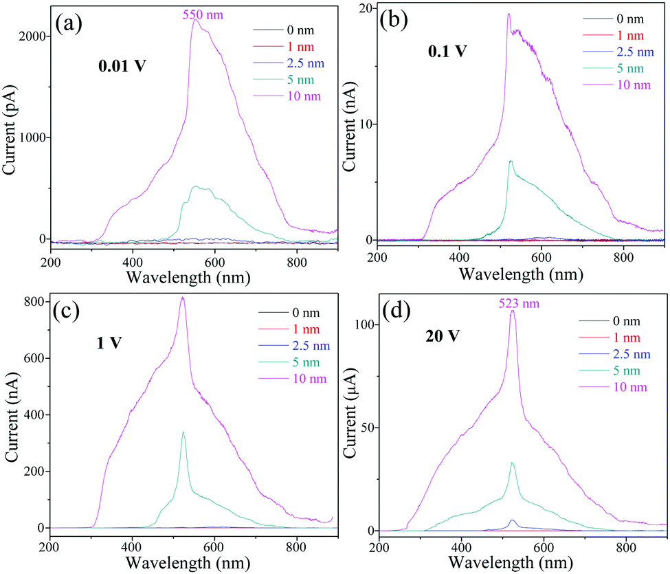 | ||
| Fig. 5 At 150 °C, the spectral response vs. wavelength at different fixed biases and illumination intensities. (a) 0.01 V; (b) 0.1 V; (c) 1 V; and (d) 20 V. | ||
After annealing at 150 °C, in addition, the influence of bias on the spectral response range selectivity was also explored at room temperature of 25 °C, as illustrated in Fig. 6. It can be seen that the photodetector still shows a below-bandgap response at the operation bias lower than 0.1 V, demonstrating a memory effect for the spectral response range. With the increase of measurement bias to 1 V, interestingly, its response to above-bandgap light is also restored. Similarly, the device shows a response to light with wavelength ranging from 280 to 800 nm besides a narrow strong bandgap light of 510 nm at measurement bias of 20 V, suggesting that the stored information of spectral response range can be erased after applying a relatively large bias.
 | ||
| Fig. 6 After annealing at 150 °C, the room temperature spectral photoresponse of detector vs. wavelength at different fixed biases and illumination intensities. (a) 0.1 V, (b) 1 V, (c) 10 V, and (d) 20 V. | ||
3.4. Mechanism of spectral response range tunability with memory characteristics
In order to identify the authentic origin of spectral response range selectivity with a memory feature, for the single NB-based two-terminal device, its I–V characteristics were measured under illumination of different sites, as shown in Fig. 7. It can be seen that the forward current shows a huge increase compared with the reverse current when the vicinity of the end connected with the negative electrode is illuminated, while it is just opposite when the vicinity of the end connected with the positive electrode is illuminated. In addition, the forward and reverse currents both show a tremendous increase when the entire device, including two electrodes, is illuminated. | ||
| Fig. 7 I–V characteristics of the photodetector at room temperature with illumination of different sites, showing asymmetrical increase in the reverse direction when only illuminating near one end electrode. (a) Only illuminating near the end connected with the negative electrode; (b) only illuminating near the end connected with the positive electrode; (c) illuminating entire device including two electrodes; (d) in the dark. | ||
At an asymmetrical temperature between the two terminal electrodes, meanwhile, the I–V characteristics were also researched by only heating the end connected with the positive electrode at different temperatures, as illustrated in Fig. 8. For the positive electrode end with a higher temperature, the reverse-biased current first increases at temperatures lower than about 100 °C, and then decreases with further increasing temperature. At 150 °C, the reverse-biased current is close to zero, resulting in the formation of diode-like current with a rectification ratio of about 200 at ±3 V. At 200 °C, however, the I–V curve becomes almost a symmetrical structure at forward and reverse bias voltage, although the current is very low. Combing the experimental results with asymmetrical illuminating and heating, it can be concluded that this unique spectral response range selectivity with memory feature is related to the trapped electrons in the surface depletion region.
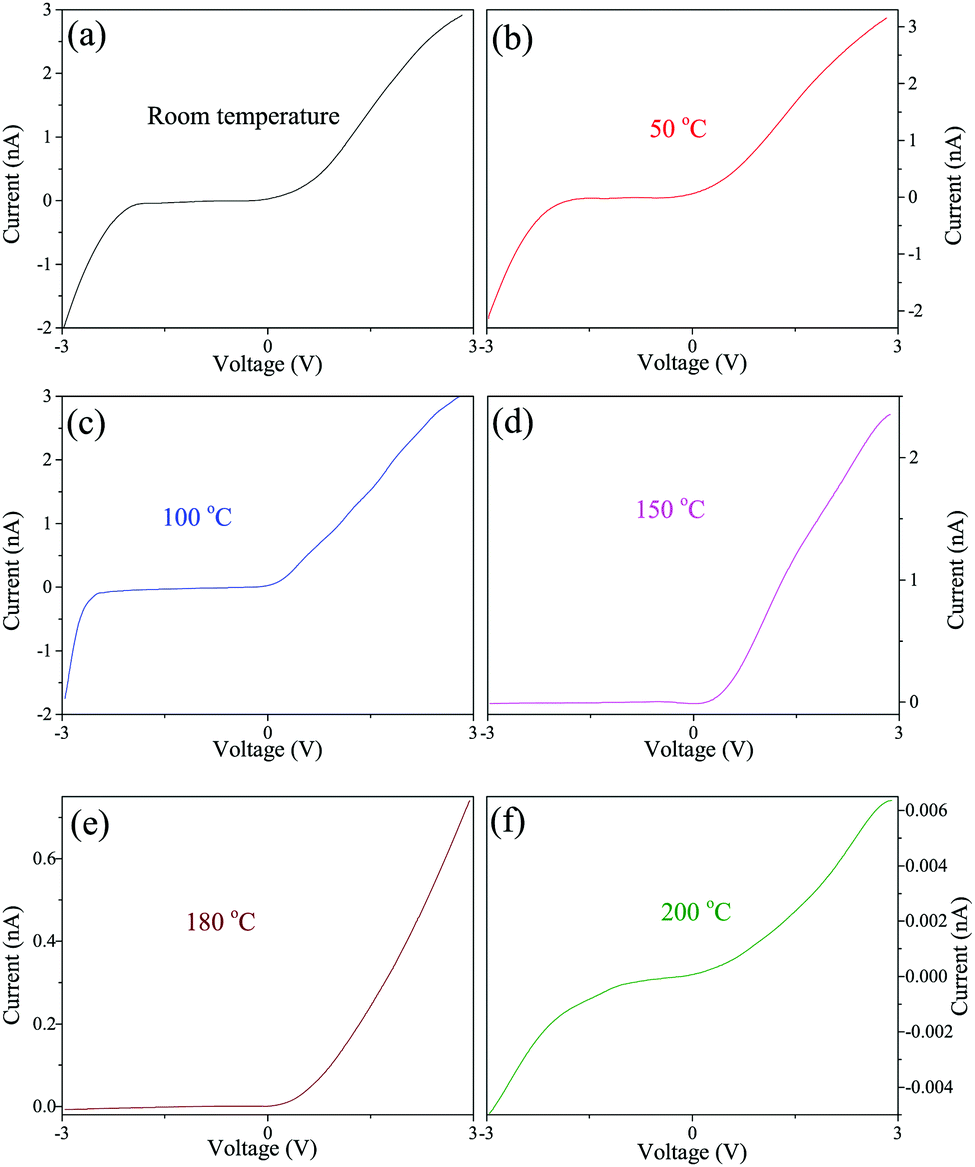 | ||
| Fig. 8 I–V characteristics of the CdS NB-based detector in dark at different temperatures when only annealing the end connected with positive electrode, showing asymmetrical decrease of current at reverse-biased voltage at temperature ranging from 100 to 180 °C. (a) Room temperature of 25 °C; (b) 50 °C; (c) 100 °C; (d) 150 °C; (e) 180 °C; and (f) 200 °C. | ||
To gain more insight into the photoresponse mechanism of CdS NB, we selected an individual NB with relatively large length and width and then conducted direct observation of its emission using a LSCM at different temperatures, as illustrated in Fig. 9. The applied laser wavelength was 405 nm, which is higher than the energy gap of CdS. From the fluorescent images, it can be seen that relatively strong blue and sky-blue emissions both exist at room temperature, and then the blue emission disappears and yellow-green is dominant at 150 °C. However, the blue emission appears again at 250 °C. The results verify firmly that the variation of photoresponse with temperature should arise from the variation of trap filling rather than bandgap narrowing induced by temperature.
 | ||
| Fig. 9 Fluorescent images of an individual CdS NB-based device measured by LSCM At different temperatures. (a) Room temperature; (b) 150 °C; and (c) 250 °C. | ||
For CdS NBs, quantities of acceptor-type surface states exist owing to the huge surface-to-volume ratio and typical n-type properties, resulting in a band bending upward and an existence of a carrier-depletion layer in the vicinity of surfaces, where majority carriers (electrons) are almost depleted completely, and correspondingly surface barriers are formed. For the two-terminal devices with Ag electrodes, two back-to-back connected diodes with series resistance are formed. In addition, quantities of stacking defects also exist in the lattice of NBs, verified by the HRTEM observation, resulting in the formation of different levels of traps. At room temperature and low operation bias, in general, the height of traps (ϕ) is higher than that of the band bending (Vd). For the conduction mechanism of a single NB under illumination of visible light, the bulk trap-related P–F hopping is predominant compared with the surface barrier between the NB and the electrodes, as illustrated diagrammatically in Fig. 10a. Accordingly, the I–V curves can be fitted well by the P–F hopping mechanism. Under a relatively large bias, however, the height of the energy band tilt in the depletion region can exceed that of the traps, which in turn gives rise to an injection of electrons into traps from the negative electrode. As a consequence, the impact of the surface barrier will surpass the hopping of the trapped electrons. Meanwhile, the height and width of the surface barrier connected with the negative electrode decrease. Especially for the tremendous reduction of the surface barrier width, the thermion emission will become a dominant conduction for the surface barrier. At 20 V operation bias, therefore, the I–V curves show a saturation tendency at higher bias under illumination, and the corresponding schematic diagram is shown in Fig. 10b.
 | ||
| Fig. 10 Schematic diagram of the response mechanism of a single CdS NB-based photodetector under different conditions. ϕ and Vd represent the height of the trap barrier and band bending, respectively. Ec, EV, Ei and Ef correspond to the conduction band, valence band, intermediate and Fermi level, respectively. (a) Under an equilibrium state or low operation bias at room temperature, showing that the surface barriers are formed at two ends for the two-terminal device, and moreover the conduction is predominant by the hopping of trapped electrons since the height of the trap (ϕ) is larger than that of band bending (Vd). (b) Under a large bias, the traps near the negative terminal are filled, resulting in a huge decrease of surface barrier height and width, the conduction is predominant by a thermion emission-controlled mechanism when illuminating the vicinity of the negative electrode end at room temperature. (c) At a moderate temperature ranging from 100 to 200 °C, trapped electrons can easily be excited thermally, and therefore electrons can directly transit from the valence band to the bottom of electron traps. (d) At a relatively high temperature, traps are completely emptied owing to thermal excitation, the generation of electrons only arises from an intrinsic excitation of CdS. | ||
For incident light, the shorter the wavelength, the larger the absorption coefficient, namely a shallower penetration depth. In general, quite a few traps are unfilled at a low operation bias and room temperature, and therefore the surface barrier is not too wide. Some of the incident light can penetrate the depletion region to reach the core of NBs, and the photoresponse is determined by both the depletion region and the core of the NBs. Hence, the photodetector can show a strong response to above-bandgap light, accompanied with a weak response to below-band light. At 20 V bias, however, the surface barrier, connected with the negative electrode, becomes extremely thin due to trap filling, and almost all incident light can penetrate the thin depletion region. Accordingly, the influence of surface barriers can be ignored, and the photoresponse is almost completely dependent on the core of the NBs. Moreover, the influence of overfilled traps can be ignored. At 20 V bias, consequently, the detector shows an exceedingly wide photoresponse ranging from 300 to 800 nm besides a strong response to green light close to the CdS bandgap energy.
With increasing measurement temperature at relatively low bias, the trapped electrons can be excited thermally, namely thermal ionization. The width and height of the surface barriers increase. It is difficult for the incident light to penetrate the depletion region, where the incident light can be absorbed completely, and hence the photoresponse only arises from the depletion region. In the depletion region, free carriers are almost completely depleted, and moreover the electrons localized in traps are also excited thermally. It is much easier for the above-bandgap light to recombine with traps. For the below-bandgap light, nevertheless, it is not easy to recombine with traps. Additionally, the electrons can be freely excited thermally from the bottom of the traps into the conduction band. After the photoexcited electrons only transit from the top of the valence band to the bottom of traps, so they can become free carriers. Therefore, the detector can show a strong photoresponse to below-bandgap light at temperatures ranging from 100 to 200 °C. Due to the complete emptying of traps at 150 °C, the surface barrier is intensely wide, and the conduction is controlled by carrier diffusion rather than thermion emission and trapped electron hopping at a low operation bias. Therefore, the I–V curves cannot be fitted well by the P–F mechanism, and moreover the responsivity is relatively low. However, the device still shows a response to the above-bandgap light owing to trap filling at a relatively large bias of 20 V.
When the measurement temperature is higher than 200 °C, the intrinsic excitation increases rapidly, resulting in a tremendous increase of free carrier concentration. Moreover, the electrons are also free in traps owing to thermal excitation. The increase of free carrier concentration is more obvious although the mobility decreases slightly due to lattice thermal vibration, and hence the width and height of the depletion region decrease again. Some of the incident light penetrates the depletion region to reach the core of NBs, and therefore the photoresponse to above-bandgap light can increase again. Correspondingly, I–V curves show a symmetrical structure although their photocurrent is relatively low compared with room temperature. After measuring at a relatively high temperature, the emptied traps cannot be filled in the condition of low bias and room temperature, and accordingly the response to below-bandgap light behaviour can be maintained, showing a memory effect on the below-bandgap light. At a relatively large operation bias, however, electrons can be injected into traps from the negative electrode, resulting in a filling of traps around the depletion region connected with the negative electrode. Moreover, the filled traps cannot also be emptied spontaneously at room temperature, and the modulated response to above-bandgap light can also be memorized.
For a single CdS NB-based photodetector, its spectral response range can not only be modulated accurately by temperature and bias, but the stored spectral response information can also be reversibly written and erased. Especially under the measurement condition of room temperature and 20 V bias, it shows an ultrahigh photoresponse performance to light to close bandgap energy compared with other CdS-based photoconductors.29–37,47–49
4. Conclusions
In summary, CdS NBs, synthesized by a thermal evaporation method, not only show a strong photoresponse to the green light close to bandgap energy with ultrahigh responsivity of approximately 107 A W−1, large photo-to-dark current ratio of 104, photoconductive gain of 107, and fast response and decay speed at 20 V operation bias and room temperature, but also show a weak photoresponse to above-/below-bandgap light. Moreover, their spectral response range shows a tunable selectivity and the corresponding photoresponse to above- and below-bandgap energy light can accurately be controlled by bias and temperature. More importantly, the modulated spectral response characteristics are well maintained at a low operation bias and room temperature, indicating a reversible writing and erasing memory effect. As the size of the materials decreases to nanoscale, they enjoy abundant surface states due to the large surface-to-volume ratio, resulting in the formation of two back-to-back connected diodes with series resistance for the two-terminal devices. Moreover, the presence of quantities of stacking faults in the NB lattice gives rise to the formation of trap centers. Surface states and traps play a decisive role in an ultrahigh photoresponse to the light close to bandgap energy and an erasable memory effect of spectral response range. At an appropriate high temperature and a relatively low bias, the traps can be emptied by thermal excitation, and conversely they can be filled up by electron injection from the negative electrode at a relatively large bias and a low temperature. After being modulated, the emptied traps cannot be injected at a low bias, and furthermore the filled traps cannot be excited thermally at room temperature, demonstrating a memory feature with reversible writing and erasing. The trap emptying induces the surface barrier to broaden, and hence the photoresponse only arises from the depletion region owing to the limitation of the penetration depth of incident light. Moreover, it is much easier for shorter wavelengths to recombine with traps. Therefore, the NB with emptied traps only shows a narrow photoresponse to below-bandgap light. The filled traps can induce a thin surface barrier, and the photoresponse mainly originates from the core of NBs besides the thin surface depletion region. Therefore, the device shows a wide photoresponse from UV to NIR besides a stronger response to green light close to the bandgap energy. The bias and temperature-controlled selectivity and memory of the spectral response range with superior performance make these CdS NBs a potential candidate in next-generation photodetector and photomemories.Conflicts of interest
There are no conflicts to declare.Acknowledgements
This work was financially supported by the National Natural Science Foundation of China (51571107, 51462023) and the Natural Science Foundation of Jiangxi Province (20152ACB20010, 20181BAB216008).References
- R. Frisenda, E. Navarro-Moratalla, P. Gant, D. P. D. Lara, P. Jarillo-Herrero and R. V. Gorbachev, Chem. Soc. Rev., 2018, 47, 53–68 RSC.
- A. Vezzoli, R. J. Brooke, S. J. Higgins, W. Schwarzacher and R. J. Nichols, Nano Lett., 2017, 17, 6702–6707 CrossRef CAS PubMed.
- J. L. Wang, Y. R. Lu, H. H. Li, J. W. Liu and S. H. Yu, J. Am. Chem. Soc., 2017, 139, 9921 CrossRef CAS PubMed.
- Z. Q. Tong, S. K. Liu, X. G. Li, J. P. Zhao and Y. Li, Nanoscale Horiz., 2018, 3, 261–292 RSC.
- M. L. Tsai, M. Y. Li, Y. M. Shi, L. J. Chen, L. J. Li and J. H. He, Nanoscale Horiz., 2017, 2, 37–42 RSC.
- S. Barth, F. Hernandez-Ramirez, J. D. Holmes and A. Romano-Rodriguez, Prog. Mater. Sci., 2010, 55, 563–627 CrossRef CAS.
- F. X. Liang, J. Z. Li, Z. P. Wang and L. B. Luo, Adv. Opt. Mater., 2017, 5, 1700081 CrossRef.
- R. S. Devan, A. R. Patil, J. H. Lin and Y. R. Ma, Adv. Funct. Mater., 2012, 22, 3326–3370 CrossRef CAS.
- M. I. Utama, J. Zhang, R. Chen, X. Xu, D. Li, H. Sun and Q. Xiong, Nanoscale, 2012, 4, 1422–1435 RSC.
- F. Wang, A. Dong and W. E. Buhro, Chem. Rev., 2016, 116, 10888–10933 CrossRef CAS PubMed.
- Y. Xia, P. Yang, Y. Sun, Y. Wu, B. Mayers, B. Gates, Y. Yin, F. Kim and H. Yan, Adv. Mater., 2003, 15, 353–389 CrossRef CAS.
- W. X. Ouyang, F. Teng and X. S. Fang, Adv. Funct. Mater., 2018, 28, 1707178 CrossRef.
- P. P. Yu, K. Hu, H. Y. Chen, L. X. Zheng and X. S. Fang, Adv. Funct. Mater., 2017, 27, 1703166 CrossRef.
- H. N. Chen and S. H. Yang, Nanoscale Horiz., 2016, 1, 96–108 RSC.
- B. C. Cheng, Z. Y. Ouyang, C. Chen, Y. H. Xiao and S. J. Lei, Sci. Rep., 2013, 3, 3249 CrossRef PubMed.
- H. P. Shi, B. C. Cheng, Q. S. Cai, X. H. Su, Y. H. Xiao and S. J. Lei, J. Mater. Chem. C, 2016, 4, 8399–8406 RSC.
- R. R. LaPierre, M. Robson, K. M. Azizur-Rahman and P. Kuyanov, J. Appl. Phys., 2017, 50, 123001 Search PubMed.
- M. Liu, Y. Peng and Z. Z. Wu, Adv. Mater. Res., 2012, 476–478, 1463–1467 CAS.
- H. Zhao, Q. Zhang and Y. X. Weng, J. Phys. Chem. C, 2007, 111, 3762–3769 CrossRef CAS.
- B. C. Cheng, J. Xu, Z. Y. Ouyang, X. Su, Y. H. Xiao and S. J. Lei, J. Mater. Chem. C, 2014, 2, 1808–1814 RSC.
- S. Kar and S. Chaudhuri, J. Phys. Chem. B, 2006, 110, 4542–4547 CrossRef CAS PubMed.
- T. Wei, Y. D. Wang, L. Chen and L. Li, Small, 2017, 13, 1701848 CrossRef PubMed.
- T. F. Zhang, Z. P. Li, J. Z. Wang, W. Y. Kong, G. A. Wu, Y. Z. Zheng, Y. W. Zhao, E. X. Yao, N. X. Zhuang and L. B. Luo, Sci. Rep., 2016, 6, 38569 CrossRef CAS PubMed.
- A. Abdel-Galil, H. E. Ali and M. R. Balboul, Optik, 2017, 129, 153–162 CrossRef CAS.
- H. Q. Li, X. Wang, J. Q. Xu, T. Bando, D. Golberg, Y. Ma and T. Y. Zhai, Adv. Mater., 2013, 25, 3017–3037 CrossRef CAS PubMed.
- T. Y. Zhai, X. S. Fang, L. Li, Y. Bando and D. Golberg, Nanoscale, 2010, 2, 168–187 RSC.
- Z. Fan, H. Razavi, J. W. Do, A. Moriwaki, O. Ergen, Y. L. Chueh, P. W. Leu, J. C. Ho, T. Takahashi, L. A. Reichertz, S. Neale, K. Yu, M. Wu, J. W. Ager and A. Javey, Nat. Mater., 2009, 8, 648–653 CrossRef CAS PubMed.
- L. Li, H. Lu, Z. Y. Yang, L. M. Tong, Y. Bando and D. Golberg, Adv. Mater., 2013, 25, 1109–1113 CrossRef CAS PubMed.
- K. M. Deng and L. Li, Adv. Mater., 2014, 26, 2619–2635 CrossRef CAS PubMed.
- W. Zhao, L. Li, M. Z. Xu, X. W. Wang, T. Zhang, Y. N. Wang, Z. Y. Zhang, S. J. Qin and Z. Liu, Adv. Opt. Mater., 2017, 5, 1700159 CrossRef.
- J. Xu, E. Oksenberg, R. Popovitz-Biro, K. Rechav and E. Joselevich, J. Am. Chem. Soc., 2017, 139, 15958–15967 CrossRef CAS PubMed.
- J. Xu and G. Z. Shen, Nano Energy, 2015, 13, 131–139 CrossRef CAS.
- Y. J. Dai, X. F. Wang, W. B. Peng, C. Xu, C. S. Wu, K. Dong, R. Y. Liu and Z. L. Wang, Adv. Mater., 2018, 30, 1705893 CrossRef PubMed.
- X. X. Yu, H. Yin, H. X. Li, W. Zhang, H. Zhao, C. Li and M. Q. Zhu, Nano Energy, 2017, 34, 155–163 CrossRef CAS.
- Q. W. An, X. Q. Meng and P. Sun, ACS Appl. Mater. Interfaces, 2015, 7, 22941–22952 CrossRef CAS PubMed.
- B. Jin, P. Huang, Q. Zhang, X. Zhou, X. W. Zhang, L. Li, J. W. Su, H. Q. Li and T. Y. Zhai, Adv. Funct. Mater., 2018, 28, 1800181 CrossRef.
- J. Y. Xu, E. Oksenberg, R. Popovitz-Biro, K. Rechav and E. Joselevich, J. Am. Chem. Soc., 2017, 139, 15958–15967 CrossRef CAS PubMed.
- C. Chen, Y. Zhai, F. M. Li, F. R. Tan, G. T. Yue, W. F. Zhang and M. T. Wang, J. Power Sources, 2017, 341, 396–403 CrossRef CAS.
- W. J. Lee, G. A. Umana-Membreno, J. Dell and L. Faraone, IEEE J. Photovolt., 2015, 5, 1783–1790 Search PubMed.
- J. J. Qiu, B. B. Weng, W. Y. Ge, L. L. McDowell, Z. H. Cai and Z. S. Shi, Sol. Energy Mater. Sol. Cells, 2017, 172, 117–123 CrossRef CAS.
- A. B. Wong, S. Brittman, Y. Yu, N. P. Dasgupta and P. Yang, Nano Lett., 2015, 15, 4096–4101 CrossRef CAS PubMed.
- P. G. Chavan, S. S. Badadhe, I. S. Mulla, M. A. More and D. S. Joag, Nanoscale, 2011, 3, 1078–1083 RSC.
- B. Piccione, C. H. Cho, L. K. van Vugt and R. Agarwal, Nat. Nanotechnol., 2012, 7, 640–645 CrossRef CAS PubMed.
- Z. B. Shao, J. S. Jie, T. H. Jiang, X. F. Wu, K. Li, F. F. Xia, X. J. Zhang and X. H. Zhang, Adv. Funct. Mater., 2018, 28, 1706577 CrossRef.
- R. M. Ma, L. Dai, H. B. Huo, W. J. Xu and G. G. Qin, Nano Lett., 2007, 7, 3300–3304 CrossRef CAS PubMed.
- P. C. Wu, Y. Ye, C. Liu, R. M. Ma, T. Sun and L. Dai, J. Mater. Chem., 2009, 19, 7296–7300 RSC.
- Y. L. Pei, R. H. Pei, X. C. Liang, Y. H. Wang, L. Liu, H. B. Chen and J. Liang, Sci. Rep., 2016, 6, 21551 CrossRef CAS PubMed.
- L. Li, P. C. Wu, X. S. Fang, T. Y. Zhai, L. Dai, M. Y. Liao, Y. S. Kido, H. Q. Wang, Y. Bando and D. Golberg, Adv. Mater., 2010, 22, 3161–3165 CrossRef CAS PubMed.
- D. S. Zheng, H. Fang, P. Wang, W. J. Luo, F. Gong, J. C. Ho, X. S. Chen, W. Lu, L. Liao and J. L. Wang, Adv. Funct. Mater., 2016, 26, 7690–7696 CrossRef CAS.
- G. Z. Shen, J. H. Cho, H. J. K. Yoo, G. C. Yi and C. J. Lee, J. Phys. Chem. B, 2005, 109, 9294–9298 CrossRef CAS PubMed.
- G. Z. Shen and C. J. Lee, Cryst. Growth Des., 2005, 5, 1085–1089 CrossRef CAS.
- Z. X. Yang, W. Zhong, Y. Deng, C. T. Au and Y. W. Du, Cryst. Growth Des., 2011, 11, 2172–2176 CrossRef CAS.
- G. G. Macfarlane, T. P. McLean, J. E. Quarrington and V. Roberts, Phys. Rev., 1957, 108, 1377–1383 CrossRef CAS.
- V. Mikhelashvili, R. Padmanabhan and G. Eisenstein, J. Appl. Phys., 2017, 122, 034503 CrossRef.
- G. Z. Shen, J. Xu, X. F. Wang, H. T. Huang and D. Chen, Adv. Mater., 2011, 23, 771–775 CrossRef CAS PubMed.
- S. M. Sze and K. K. Ng, Physics of Semiconductor Devices, John Wiley & Sons, Hoboken, New Jersey, USA, 3rd edn, 2007 Search PubMed.
- A. J. Chiquito, C. A. Amorim, O. M. Berengue, L. S. Araujo, E. P. Bernardo and E. R. Leite, J. Phys., 2012, 24, 225303 Search PubMed.
- F. Vietmeyer, T. Tchelidze, V. Tsou, B. Janko and M. Kuno, ACS Nano, 2012, 6, 9133–9140 CrossRef CAS PubMed.
| This journal is © The Royal Society of Chemistry 2019 |