DOI:
10.1039/C8NH00198G
(Communication)
Nanoscale Horiz., 2019,
4, 148-157
Active tuning of the Fano resonance from a Si nanosphere dimer by the substrate effect†
Received
24th July 2018
, Accepted 30th August 2018
First published on 31st August 2018
Abstract
All-dielectric materials have aroused great interest for their unique light scattering and lower losses compared with plasmonics. Generally, optical properties made by all-dielectric materials can be passively controlled by varying the geometry, size and refractive index at the design stage. Therefore, the realization of active tuning in the field of nanophotonics is important to improve the practicality and achieve light-on-chip technology in the future. Herein, we combine the high refractive index of Si and the phase transition of VO2 to form an active tuning hybrid nanostructure with higher quality factor by depositing Si nanospheres on the VO2 layer with an Al2O3 substrate. As the temperature goes up, the refractive index of the VO2 layer switches from high to low. The scattering intensity of the magnetic dipole resonance of Si nanospheres decreases differently depending on their size, while the intensity of the electric dipole resonance remains almost unchanged. Meanwhile, Fano resonances are observed in the Si nanosphere dimers with a continuous variable Fano lineshape when adjusting the temperature. Mie theory and substrate-induced resonant magneto-electric effects are used to analyze and explain these phenomena. Tuning of the Fano resonance is attributed to the substrate effect from the interaction between Si nanospheres and phase transition of the VO2 layer with temperature. These light scattering properties of such a hybrid nanostructure make it promising for temperature sensing or as a light source at the nanometer scale.
Conceptual insights
As we know, active tuning of the optical properties of nanoantennas and metasurfaces is desirable for a wide range of applications, including building optical circuits, and signal and information processing. Although all-dielectric materials exhibit lots of advantages, how to realize the active control of all-dielectric nanostructures still remains to be explored. We, for the first time, combine the high refractive index of Si nanospheres and the phase transition of a VO2 layer to form a hybrid nanostructure with higher quality factor. We have demonstrated the active tuning of the Fano resonance from a Si nanosphere dimer by the substrate effect in the visible range. We have also established that the phase change in the visible range can be described more precisely as a switch between a mid-refractive index state and a low-refractive index state. Furthermore, two different near field features of VO2 under two states can bring about different interaction situations between VO2 and Si nanospheres and realize the active control of the Fano resonance. Therefore, these findings suggest that devices based on individual phase-change materials and single-element structures will simplify the design of active photonic devices in the future.
|
Introduction
In the last decade, high- or moderate-refractive index semiconductor materials, which are also called all-dielectric materials, have aroused great interest among researchers in the field of nanophotonics.1–7 Compared with plasmonic analogues, the energy losses of all-dielectric optical resonators are much lower at the visible wavelength.1–3,8 Based on their unique light scattering and other optical properties, they are very promising to be a sort of substitution or supplement material for plasmonics in different application areas, such as directional scattering,9,10 Fano resonance,11–15 nonlinearity optic,15–17 enhanced absorption18,19 or emission19–21 and metasurfaces for realizing a wide variety of functions.22–25 Usually, the optical properties of a nanostructure will be changeless upon the completion of production, but can be passively controlled by varying the geometry, size and refractive index at the design stage.1,2,11,15,25,26 To achieve the same function at different wavelengths or under other specific conditions, one may need to redesign and manufacture the structure and device, which will require major expenditure of time, effort and resources. Therefore, the active controlling of a nanostructure makes a lot of sense to improve the practicality and achieve light-on-chip technology in the future.27–31
To date, there are many groups that have turned their focus to this research item and carried out lots of demonstrations about it. For instance, Yan et al. realized the spectral tailoring of a hybrid dielectric-metal nanoantenna through changing the applied voltage to alter the carrier concentration of the silicon nanoparticle.30 Based on voltage-controlled assembly, Montelongo et al. first reported a reversible electrotunable liquid mirror that can be switched from a refractive mirror to a transmissive window.31 As another example, by modifying the excitons in two-dimensional materials which are sensitive to the temperature, Wen et al. demonstrated active control over the strong coupling between gold nanorods and tungsten sulfide.28 However, the strategy most frequently adopted to realize active tuning is combining nanostructures with liquid crystals, which provide a dielectric environment tuned by their phase transition.21,22,32 Apart from the above-mentioned methods, some researchers have focused on the exploration of optically tunable and mechanically tunable all-dielectric Huygens’ metasurfaces to meet various needs of applications.9,33
Vanadium dioxide (VO2) is one of the most interesting and important materials due to the huge difference in electric and optical properties between the monoclinic phase and rutile phase,34 which makes it widely used in recent tunable nanophotonics devices. This insulator-metal phase transition in VO2 usually occurs around 68 °C.29,34 To be specific, these unique features open up the use of VO2 in modulators, color generation,24 smart windows29 and so on. Unfortunately, the refractive index of VO2 only undergoes a little change at the visible wavelength (Fig. S1a and b, ESI†), which makes it difficult to be directly used as a film in an active controlled nanostructure.24 To address this problem, one of the possible ways is to transform a film into a metasurface to support some kinds of resonances.35,36 Even so, the nanostructures made by VO2 have a low quality factor of resonance since its refractive index is not high enough (just about 3). Hence, it seems that combining VO2 with other materials with a higher permittivity will be a more realistic implementation.24,29
Among various semiconductor materials, silicon (Si) is one of the most abundant elements on the earth and especially suited as a building block in the electro-optic field.4,9,11,18–20,37 Its high refractive index (up to 4) is beneficial for forming a strong resonance with a higher quality factor, despite the low absorption losses in the visible region (Fig. S1c and d, ESI†).2,3,37 An individual Si nanoparticle in a free space is a nanoresonator supporting multiple resonances, which can be well described by Mie theory.4 As the most basic research model, Si nanospheres have been heavily used in many fields, such as nanoantenna,4 waveguides,38 sensors,39 and resonant cavities for enhancing the light–matter interaction.19,20,40 Since dielectric nanoparticles are sensitive to the refractive index of the surrounding environment, it is positive that the induction of a considerable refractive index substrate will modify the light scattering from the silicon nanoparticles.41,42
In this contribution, we propose an active tuning hybrid nanostructure by depositing Si nanospheres on a VO2 thin layer to make use of each of their advantages. The VO2 layer is fabricated by a pulsed-laser deposition (PLD) method and the Si nanospheres are acquired by femtosecond laser ablation in liquids (fs-LAL) technology as done in our previous studies.11 Individual Si nanospheres with different diameters on the VO2 layer emit rainbow colors indicating that they supports resonance at different wavelengths, just like on the SO2 substrate. When the temperature increased from 25 °C to 80 °C, the scattering intensity of the magnetic dipole (MD) resonance of the Si nanospheres will decrease differently depending on their size, while the intensity of electric dipole (ED) resonance remains almost unchanged. We use Mie theory and substrate-induced resonant magnetoelectric effects to describe and analyze the change in backward scattering spectra. The simulations have a similar trend with experimental results. Based on the result of the individual nanospheres, we measure the backward scattering spectra of Si nanosphere dimers on the VO2 layer under different temperatures, which show as a lineshape of Fano resonance with different Fano asymmetric parameters q. In addition, the famous Fano formula is used to fit the experimental results and obtain the Fano parameter q. We demonstrate that the Fano resonance of Si nanosphere dimers can be tunable through changing the refractive index of the VO2 layer which is sensitive to temperature. These light scattering properties of such a hybrid nanostructure mean that it can be used as a temperature sensor. Since the phase transition of VO2 can be triggered by different applied electric currents, the hybrid nanostructure could act as a nanoscale light source with tunable illumination intensity or a nanoantenna for information processing.
Experimental and calculation section
Fabrication and characterization
The polycrystalline VO2 thin film was fabricated by a PLD method. During the fabrication, a vanadium metal (99.99% purity) target was ablated by a KrF excimer laser pulse with a pulse rate of 4 Hz and a pulse width about 25 ns. Before the deposition process, the Al2O3 (0006) substrate was kept at 550 °C in a vacuum chamber under pressure of 4.0 Pa with flowing O2 (45 sccm) and Ar2 (30 sccm). To form this VO2 thin film, the HV and the number were set as 25 kV and 12![[thin space (1/6-em)]](https://www.rsc.org/images/entities/char_2009.gif) 000. Si nanoparticles were prepared by fs-LAL technology with pulse energy of 4 mJ and a pulse width about 35 fs. After 10 min of focused laser ablation on a monocrystal Si substrate in deionized water, the solution containing Si nanoparticles was collected. After more than 10 min ultrasonic dispersion, several drops of solution were removed onto the surface of VO2 film. In this work, the scanning electron microscope (SEM) images were taken by an FIB-SEM crossbeam workstation (Carl Zeiss, Auriga-4523) with an extremely high electrical voltage of 3–5 kV. The room-temperature X-ray diffraction (XRD) testing was performed by an LIFM-X ray powder diffractometer. The thickness of the VO2 film was confirmed by atomic force microscopy (AFM, Bruker, dimension fastscan bio). To study the hybrid nanostructure under different temperatures, the whole structure was put on an electrical microheater which can be turned from room temperature to about 80 °C.
000. Si nanoparticles were prepared by fs-LAL technology with pulse energy of 4 mJ and a pulse width about 35 fs. After 10 min of focused laser ablation on a monocrystal Si substrate in deionized water, the solution containing Si nanoparticles was collected. After more than 10 min ultrasonic dispersion, several drops of solution were removed onto the surface of VO2 film. In this work, the scanning electron microscope (SEM) images were taken by an FIB-SEM crossbeam workstation (Carl Zeiss, Auriga-4523) with an extremely high electrical voltage of 3–5 kV. The room-temperature X-ray diffraction (XRD) testing was performed by an LIFM-X ray powder diffractometer. The thickness of the VO2 film was confirmed by atomic force microscopy (AFM, Bruker, dimension fastscan bio). To study the hybrid nanostructure under different temperatures, the whole structure was put on an electrical microheater which can be turned from room temperature to about 80 °C.
Dark-field scattering spectral measurement
The dark-field (DF) backward scattering spectra of the nanostructures in this work were obtained by utilizing a dark-field optical microscope (BX51, Olympus) integrated with a quartz-tungsten-halogen lamp (120 W) with a cooled CCD camera (PiXis 400B-eXcelon, Princeton Instruments) next to it. In addition, the incident white light which was non-polarized irradiated the whole structure from an objective lens (magnification: 100, numerical aperture: 0.80) with an incident angle of 53 degree. Then the scattered light was collected by the same objective and sent to the spectrograph with a slit in front of it. To obtain S- or P-polarized light, a linear polarizer was added into the light path. Without special emphasis, the incident light was non-polarized.
Numerical simulation
The simulations including far-field backward scattering spectra and electromagnetic field amplitudes were carried out using a Finite-difference time-domain (FDTD) method. In the calculation model, a sphere whose size is determined by the SEM images was centered. By adding a semi-infinite substrate below the sphere, we could calculate the spectra in this work. The simulation area was meshed in three-dimensions (360 × 360 × 360 nm) composed of 2 nm cubic cells. In this case, we used two plane wave light sources (two electric fields were parallel to the x-axis and y-axis respectively) with normally incidence to the structure. This substitution of light sources proved simpler and more efficient without large deviation from the experimental data. The complex refractive index of VO2 and Si at different temperatures was extracted from ref. 34, 43 and 44. We changed the refractive index of VO2 in the models to simulate the insulator-metal phase transition.
Results and discussion
The proposed hybrid nanostructure composed of Si nanospheres and a VO2 thin layer is shown in Fig. 1a. The VO2 layer used in this work was grown on Al2O3 substrates by PLD and Si nanospheres were deposited onto the VO2 layer by self-assembly. To explore the optical properties of the hybrid nanostructure under different temperatures, the whole structure was put onto a microheater which can be tuned from 25 °C to 80 °C. Before combining the Si nanospheres and VO2 layer, we first investigated the properties of the VO2 layer. Fig. 1b shows the SEM image of the VO2 layer, which is featured by many small nanoparticles on its surface indicating that the sample is polycrystalline. For later analyses, the thickness of the VO2 layer was measured by AFM, which is shown in Fig. 1c. The right region represents the VO2 layer which is about 40 nm thick with a small roughness. Then the VO2 layer was characterized by room-temperature XRD with respect to the Al2O3 substrate. From Fig. 1d, it is evident that the VO2 layer has an orientation of (020) while the orientation of the Al2O3 substrate is (0006). To assess the phase-transition behavior of the VO2 we prepared, we measured the resistance between two points on the surface of the VO2 layer when heating the sample from 25 °C to 80 °C. The measurement results in Fig. 1e exhibit a hysteresis centered around 50 °C with a small hysteresis width of about 5 °C, which is suggestive of increased structural homogeneity and compactness, with little variation in grain size, crystallographic domain orientations and strain.24
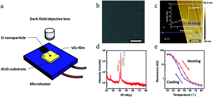 |
| | Fig. 1 Schematic illustration of the hybrid nanostructure and the properties of the VO2 layer. (a) Hybrid nanostructure including Si nanospheres and a thin VO2 layer below it, and the whole structure is put onto a microheater. (b) SEM image, (c) AFM image, (d) XRD spectrum and (e) electrical properties of the VO2 layer we fabricated in this work (the scale bars in SEM and AFM images are 300 nm and 2 μm, respectively). | |
To explore the Si nanosphere dimers on the VO2 layer, we first study the optical properties of single nanospheres. Due to the high refractive index of such Mie resonators and according to the relationship λ ≈ nd,4 the diameter of the particles we chose to study is about 100 nm to 200 nm to make sure the resonant wavelength will be confined in the visible region. Diameter, SEM images, DF images, experimental backward scattering spectra and the corresponding simulated results are displayed in Fig. 2. With the increase of diameter, the silicon nanospheres generate different colors ranging from blue, to green, yellow, orange and red, which correspond to different wavelengths of their strong magnetic and electric dipole scattering. To understand this observation in dark-field images, we performed the backward scattering spectrum measurement based on these five representative Si nanospheres on the VO2 layer with the Al2O3 substrate, whose diameters confirmed by SEM images are 107.2 nm, 126.4 nm, 155.2 nm, 170.2 nm and 187.6 nm respectively. As it can be seen from the blue lines in Fig. 2c, the backward scattering spectra are mostly dominated by the MD and ED resonances. When the nanoparticles get larger, the MD and ED resonances will shift to the long-wavelength spectral side. Typically, when the nanospheres are large enough, the higher order resonant modes such as magnetic quadrupole (MQ) and electric quadrupole (EQ) gradually appear in the short-wavelength region, just as the experimental phenomenon in previous work.45 The wavelength of the strongest resonant peak of each Si nanosphere matches their color observed in the backward direction. Using the same structures and parameters, we theoretically calculated the backward scattering spectra, which are displayed as celesta lines in Fig. 2d and well correspond to experiments. After that, a voltage was applied on the microheater below the whole hybrid nanostructure to heat it up to 80 °C directly. When the temperature settled down, we repeated the spectra measurement for these five Si nanospheres. Their backward scattering intensity has decreased differently. For each particle, the decreasing degree of MD resonance is always larger than that of ED resonance which remains nearly unchanged. As for the large particles, the decreasing degree of their MD is larger than that of smaller nanoparticle and the wavelength of MD resonance exhibits a slight blue-shift. Similarly, we preformed the calculation again to simulate the insulator-metal phase transition through changing the refractive index of VO2. The latest simulations presented as orange lines in Fig. 2d have a similar trend with experimental phenomena including an alike spectral lineshape and decreasing scattering intensity. To determine whether the properties of Si nanospheres were changed by the increased temperature, we performed a contrast experiment by replacing the VO2 layer on the Al2O3 substrate with a SiO2 substrate which is very stable. The experimental results (Fig. S2, ESI†) suggest that the Si nanospheres with a diameter ranging from 132.9 nm to 201.6 nm won’t be affected by the temperature change. Also, the complex refractive index of Si at 20 °C and 100 °C also confirms this point (Fig. S1, ESI†).
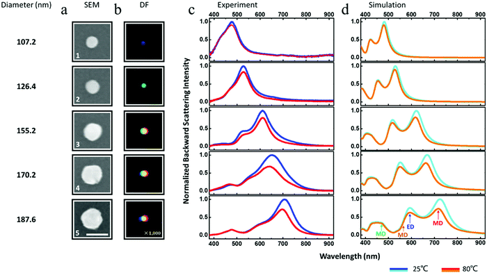 |
| | Fig. 2 Experimental and simulated backward scattering spectra of a single Si nanosphere on the VO2 layer. (a) SEM images, (b) DF images, (c) experimental and (d) simulated normalized backward scattering spectra of a single Si nanosphere with a diameter of 107.2 nm, 126.4 nm, 155.2 nm, 170.2 nm and 187.6 nm (the scale bar in the SEM images is 200 nm and the magnification of the optical microscope is 1000). | |
As mentioned above, it seems that the decreasing degrees become larger with the increase of diameter. Therefore, we measured twenty other Si nanospheres with different diameters (see Fig. S3, ESI†) and plot their change in Fig. 3a, which approaches a linear relationship approximately. The different decrease originates from the different changing degrees of the refractive index of VO2 at different wavelengths and the different values of scattering cross section for different particles. It is noteworthy that the phase transition of the VO2 layer is reversible, and we measure particle 4 for three cycles to test the reversibility of our active controlled hybrid nanostructure. As shown in Fig. 3b, the hybrid nanostructure exhibits reversiblity to some extent after heating and cooling several times. Finally, based on the same particle 4, we observed a continued changing process by varying the applied voltage on the microheater to heat the structure to different target temperatures, which is presented in Fig. 3c. Compared with the scattering intensity of MD resonance at 25 °C, it falls from 1 to 0.6 at 80 °C. As for that of ED resonance, this value falls from 0.4 to 0.3 for the same process.
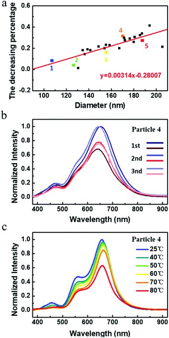 |
| | Fig. 3 More optical properties of the hybrid nanostructure based on a single Si nanosphere. (a) The decreasing percentage of light scattering intensity of MD resonance of 25 particles with different diameters during the phase transition of a VO2 layer. (b) The reversibility and (c) continuous tunability from particle 4. | |
To theoretically investigate this influence, we first consider a single Si nanosphere on different kinds of supporting substrates. The calculated backward scattering spectra of an individual Si nanosphere with a diameter of 170 nm deposited on different substrates are shown in Fig. 4a. As described by Mie theory, the light scattering of sub wavelength dielectric particles can be analyzed by dipole approximation,4
where
p1 and
m1 are the effective electric and magnetic dipole moments,
ε0 is the vacuum permittivity,
αE and
αH are the effective polarizabilities,
E0 and
H0 are the electric and magnetic fields of the incident light, and
a1 and
b1 are the Mie's dipole scattering coefficients. The calculated scattering cross section of a Si nanosphere under vacuum is plotted as a black line in
Fig. 4a. Two resonances located at about 550 nm and 700 nm represent the MD and ED resonances. For the MQ and EQ resonances located at about 450 nm and 520 nm, we will neglect them since they are far away from the MD and ED resonances and of weak strength, so they won’t make a big difference to the analysis and discussion.
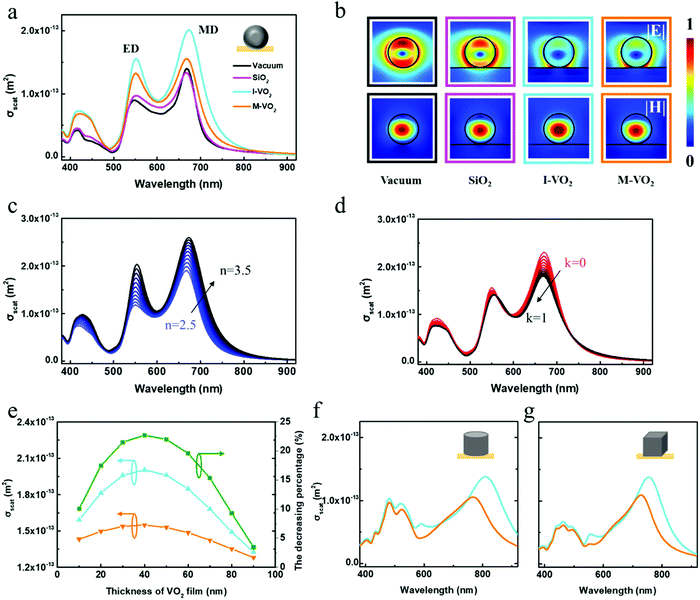 |
| | Fig. 4 Theoretical analysis of the substrate effect on a single subwavelength dielectric particle. (a) Simulated backward scattering spectra and (b) normalized electromagnetic field amplitudes at MD resonance of a Si nanosphere with a diameter of 170 nm on different kinds of substrates. (c) Calculated scattering cross section as a function of wavelength of a Si nanosphere with a diameter of 170 nm on a fictitious substrate with 2.5 ≤ n ≤ 3.5 and k = 0, in index steps of 0.1. (d) Calculated scattering cross section for the same particle in (c) on another fictitious substrate with n = 3 and 0 ≤ n ≤ 1, in index steps of 0.1. (e) Influence of a VO2 layer toward active control for a Si nanosphere with a diameter of 170 nm. (f) Calculated backward scattering spectra of a Si nanodisk with a bottom diameter and height of 170 nm and (g) a Si nanocube with a side length of 170 nm on the same VO2 layer as (a). | |
Then the same nanoparticle is put onto a SiO2 substrate, whose spectra are the purple lines in Fig. 4a. This is no big difference compared with the situation when the particle is under vacuum. When the particle is transferred to a 40 nm-thick insulator-phase VO2 layer with the Al2O3 substrate, however, the spectrum has changed obviously with an increasing scattering cross section at both ED and MD resonances. On inspection, it is not only the change in the refractive index of the supporting substrate that leads to the spectral difference since the particle and the supporting film have an extremely small contact point. Hence, we assume that this substrate effect mainly originated from the image dipoles in the supporting film induced by the dipole moments of the nanoparticles. When the refractive index of a substrate is high enough, the substrate will couple to the particles near it and the substrate-induced resonant magnetoelectric effects should be considered. In this situation, the image dipoles will apply an additional electric and magnetic field as a feedback to the particles. As a result, eqn (1) and (2) will be modified a little by taking the additional fields into consideration,42
| | p1 = ε0![[small alpha, Greek, circumflex]](https://www.rsc.org/images/entities/i_char_e101.gif) EEE0 + ε0EMH0 EEE0 + ε0EMH0 | (5) |
| | | m1 = MMH0 + MEE0 | (6) |
where
EE,
EM,
MM and
ME are the modified effective polarizabilities. The calculated normalized electromagnetic field amplitudes of a single Si nanosphere with different substrates at MD resonance are given in
Fig. 4b. Compared with the nanoparticle under vacuum, the electric and magnetic fields near a particle with the SiO
2 substrate are almost the same. The electric fields are mostly distributed on two sides of the nanoparticle while the magnetic field is inside it. It is different that the electric field concentrates at the contact point between the Si nanosphere and insulator-phase VO
2 layer while the magnetic field profile inside the particle starts to increase. Based on the above discussion, hence, we think that it is the coupling between the Si nanospheres and the supporting substrate that also contributes to the spectral difference. However, if the same nanoparticle is deposited on a metal-phase VO
2 layer, the scattering cross section of ED and MD resonances will decrease to different degrees. We attribute this to the different changes of refractive index of a VO
2 layer at different wavelengths during the phase transition and the sensibility of ED and MD resonances. To understand this process,
Fig. 4c shows the scattering cross section for the same resonator on a fictitious substrate with an imaginary part of the refractive index
k = 0 and a real part in the range from 2.5 to 3.5, varying in steps of 0.1. The scattering cross sections of ED and MD resonances have almost the same decrease when increasing the index of the substrate. A small shift to the short-wavelength spectral side is observed for both the ED and MD resonances. Compared with a cylinder resonator, the valve of blue-shift of resonant wavelength is smaller because of the smaller contact point and most light is limited inside the resonator which is not as sensitive to the index of the substrate as the plasmonics.
41 In the same way, we discuss the influence of the imaginary part of the refractive index of the substrate by putting the same resonator on another fictitious substrate with a real part of the refractive index
n = 3 and an imaginary part in the range from 0 to 1, varying in steps of 0.1. Interestingly, the profile of MD modes reduces significantly while the ED modes remain nearly unchanged. By the above analysis and discussion, taking the change rule of the real and imaginary part of the refractive index of VO
2 during the phase transition (the decreases of
n and
k get higher with increased wavelength, see Fig. S1, ESI
†) into consideration, the scattering intensity of MD resonance reduces a lot while the phase transitions of VO
2 have a small impact on that of ED resonance at the visible wavelength. In addition, we calculated the same nanosphere on a VO
2 layer with different thickness to determine how the thickness influences the active control in this case, which is summarized in
Fig. 4e (more details in Fig. S4, ESI
†). In the beginning, the scattering cross section of MD resonance increases with the thickening of the VO
2 layer. It reaches the maximum when the thickness is 40 nm and declines for a thicker VO
2 layer. To a certain extent, a 40-thick-VO
2 layer is the optimum for a Si nanosphere with a diameter of 170 nm. The decreasing percentage of scattering cross section when the VO
2 layer changes from an insulator-phase to metal-phase has a maximum of 22.7%. In the same model, if the Si nanosphere is replaced by a Si nanodisk or a Si nanocube, their backward scattering spectra are similar to the former situation (
Fig. 4f and g). As mentioned above, the more contact area between them, the more obvious the change of backward scattering spectra because of the change in the refractive index of the supporting substrate. Based on that, their wavelength of MD resonance changes a lot during the phase transition of VO
2. However, considering the coupling between particle and substrate, the decreasing percentage of scattering cross section of MD resonance is 23.5% and 20.6% for the disk and cube. But, the sphere has a higher scattering cross section, which makes it advantageous to be used rather than a disk or a cube.
Then, we dealt with the Si nanosphere dimers in the same manner. Diameter, SEM images, DF images, experimental backward scattering spectra and the corresponding simulations of our studied dimers are displayed in Fig. 5. Discussed by our previous work based on Si nanosphere dimers,11 the size we chose to investigate is 128.6 nm & 128.6 nm, 125.1 nm & 138.1 nm and 137.5 nm & 150.8 nm to generate a Fano dip in the visible region. At room temperature, all three dimers produce a small Fano dip at different wavelengths depended on their size. However, the light scattering intensity goes down when the 40 nm-thick VO2 layer on the Al2O3 substrate transfers into the metal phase. In addition, the spectral line shapes change and the Fano dips become smaller. Through simulations, we observed a similar result that well corresponds with the experiment. Moreover, we repeated the measurement by using both S- and P-polarized incident light (Fig. S5, ESI†). The spectra obtained by using different polarized incident light for each dimer reveal a uniform trend.
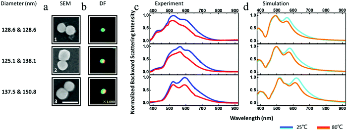 |
| | Fig. 5 Experimental and simulated backward scattering spectra of Si nanosphere dimers on the VO2 layer. (a) SEM images, (b) DF images, (c) experimental and (d) simulated normalized backward scattering spectra of a Si nanosphere dimer with a size of 128.6 nm & 128.6 nm, 125.1 nm & 138.1 nm and 137.5 nm & 150.8 nm (the scale bar in SEM images is 200 nm and the magnification of the optical microscope is 1000). | |
According to Albella's work, when two Si nanospheres on the VO2 layer start to get close to each other, another additional electric and magnetic dipole will be induced by the nearby particle, apart from that caused by the image dipole in the substrate.46 A dipole–dipole coupling model can be used to analyze this situation. If the polarization of incident light is parallel to the long axis of the dimer, the induced dipoles can be expressed in the following form:46
| | p2 = ε0εh![[small alpha, Greek, tilde]](https://www.rsc.org/images/entities/i_char_e0dc.gif) eyE0 eyE0 | (7) |
| | | m2 = −mxE0/Z | (8) |
| | | ey = αe′/(1 − αe′k2gyy) | (9) |
| | | mx = αm′/(1 + αm′k2gxx) | (10) |
where
ey and
mx are the dressed polarizabilities,
k is the wavenumber,
αe′ and
αm′ are related to the modified effective polarizabilities
EE,
EM,
MM and
ME in
eqn (5) and (6),
gxx and
gyy are scalar Green's functions related to the distances between two particles, and
Z is the vacuum impedance. Therefore, their ED resonance in each sphere couples strongly to another one to form a much broader resonant mode. While the MD resonances will reduce their resonant peak and become a little narrower after forming a dimer. As a result, these new-formed hybrid continuous ED modes and discrete MD modes overlap and generate a Fano resonance as illuminated in
Fig. 6a. Based on the above analysis, when the VO
2 layer was transferred from an insulator phase to a metal phase, the scattering intensity of the dimer reduced. And because of the different decreasing degrees of ED and MD resonances in a single nanoparticle, the lineshape of Fano resonance from a dimer changed with them.
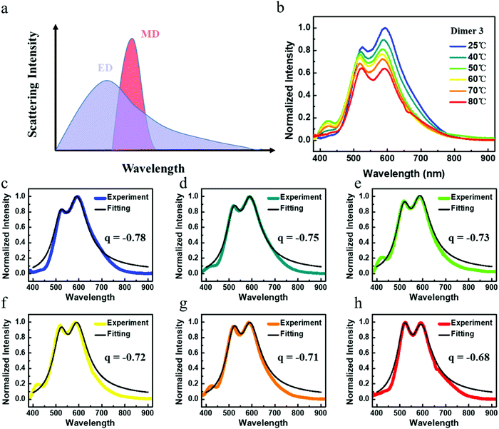 |
| | Fig. 6 Backward scattering spectra of a Si nanosphere dimer on the VO2 layer at different temperatures. (a) Illustration of the formation mechanism of Fano resonance in the Si nanosphere dimer. (b) Continuous tunability from dimer 3. (c–h) Normalized experimental scattering spectra of dimer 4 showing similar Fano lineshapes at different temperatures and the results of theoretical analysis with different fitting Fano parameter q. | |
Taking dimer 3 for example, a continued changing process can be observed by gradually increasing the applied voltage on the microheater, which is presented in Fig. 6b. To study carefully this process, we employed a simple approach including the most famous Fano formula47 and the original Fano model48 to fit the experimental results to obtain the key Fano asymmetry parameter q,
| | | σcon = a2/(1 + (2(ω − ωE)/ΓE)2) | (13) |
| | | σdis = (D2((q + Ω)2 + b))/(1 + Ω2) | (14) |
| | | D2 = 4sin2δ | (16) |
| | | q = cotδ | (17) |
where
ωE and
ωM are the resonant frequency of the ED and MD modes,
ΓE and
ΓM are the half-width of the resonance line at a half-maximum of the ED and MD modes,
q is the Fano asymmetry parameter,
a and
b are the maximal amplitude of the resonance and the damping parameter, and
δ is the phase shift of the continuum. The results of fitting are summarized in
Fig. 6c–h. From 25 °C to 80 °C, the observed spectra maintain a Fano lineshape while the Fano parameter
q increases from −0.78 to −0.68. It is evidence that the Fano resonance from Si nanosphere dimers on the VO
2 layer can be tuned by the phase transition of VO
2 which is related to temperature. Such tunable Fano resonance has a variety of applications, such as in biochemical sensing, light switch, information processing.
However, one can easily see that there are some differences between the experimental results and theoretical calculations. For the single Si nanosphere, the ED resonance in the experiment is weaker than that in the simulations because of the non-ideality of the particle shape, which has been discussed in previous work.26 Apart from the above analysis, the discrepancy between the refractive index of VO2 we prepared and that we extract from a ref. 34 is another primary cause. It is worth mentioning that the contact point is different from the ideal situation since the VO2 layer in this work does not have a perfectly smooth surface. In addition, the light source in the experiment is also different from the simulations. The oxide layer of Si nanospheres is unavoidable,4 which weakens the coupling between the particles and substrate. All these factors lead to the difference between the experiment and the simulation. In the same manner, the oxide layer of Si nanospheres increased the actual distance between two particles and weakens the coupling. At the same time, thinking again that the intensity of the continuous ED mode is weaker than the discrete MD mode, the Fano dips on the spectra are not very recognizable, which is unlike those very sharp Fano resonances.15,47 Last but not least, during the measurement, the actual temperature of VO2 will be hardly controlled accurately and a little lower than the setting object temperature. And because of personal error, there may be some difference for the same research object under the same conditions. In short, our simulation is still in good agreement with the experimental data.
Generally speaking, we use all-dielectric nanoparticles to take the place of plasmonics in this work for two main reasons. One reason is that the Fano resonance can be easily observed in all-dielectric nanosphere dimers, which is attributed to the abundant resonant modes in each single nanosphere. It is unlikely that active control of the Fano resonance will be achieved by using a metallic nanosphere dimer. As another reason, the inherent Ohmic loss will lead to Joule heating and hinder their applications considering the temperature.3,8 The use of the metallic nanosphere in our case would lower the temperature of phase-transition of VO2 and narrow the tuning range. Anyway, the utilization of VO2 destines that the active control can only work near the temperature of phase-transition of VO2. However, VO2 in this platform can be replaced by other active materials to sense different environment parameters.
Conclusions
In summary, based on PLD, LAL and self-assembly methods, we have fabricated Si nanospheres and dimers on a VO2 layer with an Al2O3 substrate. When the VO2 layer transfers from an insulator phase to a metal phase, the scattering intensity of MD resonance of an individual Si nanosphere reduces more than that of ED resonance. The prime reason is that Si nanospheres couple to the VO2 layer and the MD resonance is more sensitive to the change in the refractive index of VO2 during phase transition. According to this feature, we investigated Si nanosphere dimers in the same manner and observed a significant change in the Fano resonant lineshape. In addition, we used the famous Fano formula to fit the experimental results and got the Fano parameter q. We demonstrated that the Fano resonance generated in Si nanosphere dimers can be actively tuned by utilizing the phase transition of VO2 which is sensitive to temperature. Therefore, the light scattering properties of this hybrid nanostructure mean it can be used as a temperature sensor for healthcare or information processing. Considering that the phase transition of VO2 can be triggered by different applied electric currents directly, the hybrid nanostructure could act as a nanoscale light source with tunable illumination intensity or a nanoantenna with varying signals.
Conflicts of interest
There are no conflicts to declare.
Acknowledgements
The National Basic Research Program of China (2014CB931700), Guangzhou city (201804020074) and State Key Laboratory of Optoelectronic Materials and Technologies supported this work.
References
- S. Jahani and Z. Jacob, Nat. Technol., 2016, 11, 23 CAS.
- Y. Kivshar and A. Miroshnichenko, Opt. Photonics News, 2017, 28, 24 CrossRef.
- A. I. Kuznetsov, A. E. Miroshnichenko, M. L. Brongersma, Y. S. Kivshar and B. Luk’yanchuk, Science, 2016, 354, 2472 CrossRef PubMed.
- A. B. Evlyukhin, S. M. Novikov, U. Zywietz, R. L. Eriksen, C. Reinhardt, S. I. Bozhevolnyi and B. N. Chichkov, Nano Lett., 2012, 12, 3749 CrossRef CAS PubMed.
- A. Garcia-Etxarri, R. Gomez-Medina, L. S. Froufe-Perez, C. Lopez, L. Chantada, F. Scheffold, J. Aizpurua, M. Nieto-Vesperinas and J. J. Saenz, Opt. Express, 2011, 19, 4815 CrossRef CAS PubMed.
- Z. Yang, R. Jiang, X. Zhuo, Y. Xie, J. Wang and H. Lin, Phys. Rep., 2017, 701, 1 CrossRef CAS.
- A. E. Miroshnichenko, A. B. Evlyukhin, Y. F. Yu, R. M. Bakker, A. Chipouline, A. I. Kuznetsov, B. Luk’yanchuk, B. N. Chichkov and Y. S. Kivshar, Nat. Commun., 2015, 6, 8069 CrossRef CAS PubMed.
- J. B. Khurgin, Nat. Nanotechnol., 2015, 10, 2 CrossRef CAS PubMed.
- K. Fan, J. Zhang, X. Liu, G. Zhang, R. D. Averitt and W. J. Padilla, Adv. Mater., 2018, 30, 1800278 CrossRef PubMed.
- J. Li, N. Verellen, D. Vercruysse, T. Bearda, L. Lagae and P. V. Dorpe, Nano Lett., 2016, 16, 4396 CrossRef CAS PubMed.
- J. Yan, P. Liu, H. Wang, H. Chen, C. Wang and G. Yang, ACS Nano, 2015, 9, 2968 CrossRef CAS PubMed.
- B. Hopkins, D. S. Filonov, A. E. Miroshnichenko, F. Monticone, A. Alu and Y. S. Kivshar, ACS Photonics, 2016, 2, 724 CrossRef.
- Y. Tsuchimoto, T. Yano, T. Hayashi and M. Hara, Opt. Express, 2016, 24, 14451 CrossRef CAS PubMed.
- T. Cao, L. Zhang, Z. Xiao and H. Huang, J. Phys. D: Appl. Phys., 2013, 46, 603 CrossRef.
- P. P. Vabishchevich, S. Liu, M. B. Sinclair, G. A. Keeler, G. M. Peake and I. Brener, ACS Photonics, 2018, 5, 1685 CrossRef CAS.
- M. Shcherbakov, D. Neshev, B. Hopkins, A. Shorokhov, I. Staude, E. Melik-Gaykazyan, M. Decker, A. Ezhov, A. Miroshnichenko, I. Brener, A. A. Fedyanin and Y. S. Kivshar, Nano Lett., 2014, 14, 6488 CrossRef CAS PubMed.
- C. Ma, J. Yan and G. Yang, Nanotechnology, 2016, 27, 425206 CrossRef CAS PubMed.
- N. O. Lank, R. Verre, P. Johansson and M. Kall, Nano Lett., 2017, 17, 3054 CrossRef PubMed.
- E. Tiguntseva, A. Chebykin, A. Ishteev, R. Haroldson, B. Balachandran, E. Ushakova, F. Komissarenko, H. Wang, V. Milichko, A. Tsypkin, D. Zuev, W. Hu, S. Makarov and A. Zakhidov, Nanoscale, 2017, 9, 12486 RSC.
- A. F. Cihan, A. G. Curto, S. Raza, P. G. Kik and M. L. Brongersma, Nat. Photonics, 2018, 12, 284 CrossRef CAS.
- J. Bohn, T. Bucher, K. E. Chong, A. Komar, D. Choi, D. N. Neshev, Y. S. Kivshar, T. Pertsch and I. Staude, Nano Lett., 2018, 18, 3461 CrossRef CAS PubMed.
- J. Sautter, I. Staude, M. Decker, E. Rusak, D. N. Neshev, I. Brener and Y. S. Kivshar, ACS Nano, 2015, 9, 4308 CrossRef CAS PubMed.
- Y. F. Yu, A. Y. Zhu, R. Paniagua-Dominguez, Y. H. Fu, B. Luk’yanchuk and A. I. Kuznetsov, Laser Photonics Rev., 2015, 9, 412 CrossRef CAS.
- F. Shu, F. Yu, R. Peng, Y. Zhu, B. Xiong, R. Fan, Z. Wang, Y. Liu and M. Wang, Adv. Opt. Mater., 2018, 6, 1700939 CrossRef.
- M. Khorasaninejad, W. T. Chen, R. C. Devlin, J. Oh, A. Y. Zhu and F. Capasso, Science, 2016, 352, 1190 CrossRef CAS PubMed.
- Y. H. Fu, A. I. Kuznetsov, A. E. Miroshnichenko, Y. F. Yu and B. Luk’yanchuk, Nat. Commun., 2013, 4, 1527 CrossRef PubMed.
- A. L. Holsteen, S. Raza, P. Fan, P. G. Kik and M. L. Brogersma, Science, 2017, 358, 1407 CrossRef CAS PubMed.
- J. Wen, H. Wang, W. Wang, Z. Deng, C. Zhuang, Y. Zhang, F. Liu, J. She, J. Chen, H. Chen, S. Deng and N. Xu, Nano Lett., 2017, 17, 4689 CrossRef CAS PubMed.
- Q. Hao, W. Li, H. Xu, J. Wang, Y. Yin, H. Wang, L. Ma, F. Ma, X. Jiang, O. G. Schmidt and P. K. Chu, Adv. Mater., 2018, 30, 1705421 CrossRef PubMed.
- J. Yan, C. Ma, P. Liu, C. Wang and G. Yang, Nano Lett., 2017, 17, 4793 CrossRef CAS PubMed.
- Y. Montelongo, D. Sikdar, Y. Ma, A. J. S. Mclntosh, L. Velleman, A. R. Kucernak, J. B. Edel and A. A. Kornyshev, Nat. Mater., 2017, 16, 1469 CrossRef PubMed.
- A. Komar, Z. Fang, J. Bohn, J. Sautter, M. Decker, A. Miroshnichenko, T. Pertsch, I. Brener, Y. S. Kivshar, I. Staude and D. N. Neshev, Appl. Phys. Lett., 2017, 110, 071109 CrossRef.
- P. Gutruf, C. Zou, W. Withayachumnankul, M. Bhaskaran, S. Sriram and C. Fumeaux, ACS Nano, 2015, 10, 133 CrossRef PubMed.
- H. W. Verleur, A. S. Barker and C. N. Berglund, Phys. Rev., 1968, 172, 788 CrossRef CAS.
- F. Ligmajer, L. Kejik, U. Tiwari, M. Qiu, J. Nag, M. Konecny, T. Sikola, W. Jin, R. F. Haglund, Jr., K. Appavoo and D. Y. Lei, ACS Photonics, 2018, 5, 2561 CrossRef CAS.
- K. Sun, C. A. Riedel, A. Urbani, M. Simeoni, S. Mengali, M. Zalkovskij, B. Bilenberg, C. H. de Groot and O. L. Muskens, ACS Photonics, 2018, 5, 2280 CrossRef CAS.
- I. Staude and J. Schilling, Nat. Photonics, 2017, 11, 274 CrossRef CAS.
- R. M. Bakker, Y. Yu, R. Paniagua-Dominguez, B. S. Luk’yanchuk and A. I. Kuznetsov, Nano Lett., 2017, 17, 3458 CrossRef CAS PubMed.
- J. Yan, P. Liu, Z. Lin and G. Yang, Nanoscale, 2016, 8, 5996 RSC.
- H. Wang, Y. Ke, N. Xu, R. Zhan, Z. Zheng, J. Wen, J. Yan, P. Liu, J. Chen, J. She, Y. Zhang, F. Liu, H. Chen and S. Deng, Nano Lett., 2016, 16, 6886 CrossRef CAS PubMed.
- J. van de Groep and A. Polman, Opt. Express, 2013, 21, 26285 CrossRef CAS PubMed.
- A. E. Miroshnichenko, A. B. Evlyukhin, Y. S. Kivshar and B. N. Chichkov, ACS Photonics, 2015, 2, 1423 CrossRef CAS.
-
E. D. Palik, Handbook of Optical Constants of Solids, Academic Press, San Diego, 1998 Search PubMed.
- G. Vuye, S. Fisson, V. N. Van, Y. Wang, J. Rivory and F. Abeles, Thin Solid Films, 1993, 233, 166 CrossRef CAS.
- C. Zhang, Y. Xu, J. Lin, J. Li, J. Xiang, H. Li, J. Li, Q. Dai, S. Lan and A. E. Miroshnichenko, Nat. Commun., 2018, 9, 2964 CrossRef PubMed.
- P. Albella, M. A. Poyli, M. K. Schmidt, S. A. Maier, F. Moreno, J. J. Saenz and J. Aizpurua, J. Phys. Chem. C, 2013, 117, 13573 CrossRef CAS.
- M. F. Limonov, M. V. Rybin, A. N. Poddubny and Y. S. Kivshar, Nat. Photonics, 2017, 11, 543 CrossRef CAS.
- M. Wang, A. Krasnok, T. Zhang, L. Scarabelli, H. Liu, Z. Wu, L. M. Liz-Marzan, M. Terrones, A. Alu and Y. Zheng, Adv. Mater., 2018, 30, 1705779 CrossRef PubMed.
Footnote |
| † Electronic supplementary information (ESI) available. See DOI: 10.1039/c8nh00198g |
|
| This journal is © The Royal Society of Chemistry 2019 |
Click here to see how this site uses Cookies. View our privacy policy here. 
 and
Guowei
Yang
and
Guowei
Yang


