
Enhanced moisture stability of metal halide perovskite solar cells based on sulfur–oleylamine surface modification†
Yu
Hou‡
 ,
Zi Ren
Zhou‡
,
Tian Yu
Wen
,
Hong Wei
Qiao
,
Ze Qing
Lin
,
Bing
Ge
and
Hua Gui
Yang
*
,
Zi Ren
Zhou‡
,
Tian Yu
Wen
,
Hong Wei
Qiao
,
Ze Qing
Lin
,
Bing
Ge
and
Hua Gui
Yang
*
Key Laboratory for Ultrafine Materials of Ministry of Education, School of Materials Science and Engineering, East China University of Science and Technology, 130 Meilong Road, 200237 Shanghai, China. E-mail: hgyang@ecust.edu.cn
First published on 30th July 2018
Abstract
As one of the most promising light-harvesting materials, perovskites have drawn tremendous attention for their unique advantages, such as high efficiency, low cost and facile fabrication compared with other photovoltaic materials. Nevertheless, poor moisture tolerance of the perovskites greatly hampers the operation of such devices and hinders their commercialization. Herein, we demonstrate a facile dipping treatment using sulfur–oleylamine solution for surface atomic modulation of perovskite films. Oleylammonium polysulfides (OPs) would be self-assembled on the etched perovskite film as an ultrathin outer layer. This layer could passivate the surface chemical activity of the outer perovskite layers. Moreover, the hydrophobic OPs significantly enhance moisture stability of such devices. As a result, the obtained device without encapsulation retains more than 70% of its initial power conversion efficiency (PCE) after 14 days of exposure to a relative humidity of 40 ± 10%.
Conceptual insightsIn recent years, perovskite solar cells have reached certified power conversion efficiency (PCE) of 22.7%. However, these devices degrade rapidly in humid conditions. Developing new perovskite materials, such as 2D perovskites, is an efficient approach to tackling this drawback. However, as the length or bulk of the alkyl carbon chains increase, PCE of devices declines due to the steric hindrance. In this paper, for the first time, a sulfur–oleylamine precursor prepared at low temperature is introduced to modulate the chemical activity of perovskite film. Under the controllable pre-etching effect of H2S, smoother perovskite films can be obtained. Subsequently, the volume-dependent dipping treatment reaches equilibrium between the etching and assembling processes, leading to an enhancement in moisture stability for these devices. More importantly, devices based on such materials have shown almost no loss in energy conversion efficiency. The reaction properties of sulfur and other alkylamines are yet to be investigated. The regulation of size and shape of perovskite single crystals may be realized using this precursor. This method may also be used for the surface ligand exchange on perovskite quantum dots, which may bring exceptional results. Overall, the surface-treatment based on this method provides new insights into stable perovskite materials for optical applications. |
Introduction
The organometal halide perovskite solar cells (OHPSCs) with a ABX3 (A = alkylammonium, B = metal, X = halide) structure has been developed rapidly since its first appearance in 2009. The power conversion efficiency of these cells has already reached a certified record value of 23.3%.1,2 However, the moisture sensitivity of such perovskite materials greatly hampers their further development.3–8 Hydration of organometal halide perovskites in air is thermodynamically preferred, for example, MAPbI3 perovskites usually degrades within 3 hours under a relative humidity in the range of 70–80%.3,9 Previous research has revealed that the moisture instability of these perovskites can be attributed to the molecular absorption of water at surface Pb sites. The (100) surface of tetragonal perovskite with relatively low absorption energy is prone to interacting with water molecules, thus causing degradation of the perovskite.10To improve moisture stability of the perovskites, Ruddlesden–Popper type perovskite materials with layered structures have been developed, which impede ion migration and prevent the lattice from collapsing inside.11 Innovatively, Li et al. added gallium acetylacetonate to the perovskite precursor solution.12 The isomer of gallium acetylacetonate aggregates in the grain boundaries and surrounds the perovskite grain, thus forming a core/shell structure that protects the perovskite from moisture. Although the above-mentioned structural adjustments can enhance the moisture stability of perovskites effectively, the accompanying incrementally disordered structure will impede carrier transport and impair the performance of OHPSCs.11 Moreover, numerous studies have focused on emerging metal oxides (SnO2,13 Al2O314) and binary chalcogenides (In2S3,15 ZnSe16) as replacements for traditional electron/hole transport materials, and the devices based on these materials exhibit benign operation stability.
Besides the abovementioned methods, surface modification of perovskites is also employed as a novel strategy for its interfacial optimization while having limited impact on the bulk material. The perovskite surface is passivated by introducing functionalized molecules or polymers, which prevent the perovskite from erosion by water molecules as well as facilitate electron/hole extraction between the perovskite and the electron/hole transport layer (ETL/HTL). After surface modification, lattice defects can be significantly reduced, which results in lower charge recombination and enhanced device performance.17,18 It is demonstrated that long chain alkyls or aromatic rings, such as alkylphosphonic acid ammonium,19 polystyrene17 and polytetrafluoroethylene,20 can interact with perovskites by crosslinking, thus suppressing the lattice plane interactions with water molecules and enhancing the moisture tolerance of such devices. By forming Pb–S bonds, thiourea can passivate the perovskite film and achieve excellent stability after 60 days of operation.21 Hydrophobic alkylammonium cations were assembled onto the perovskite surface via dipping method, and the obtained devices exhibited exceptional moisture stability under a high relative humidity over 90% after more than 30 days.10 Although Organic molecules or polymers anchored on the perovskite surface effectively improve moisture stability of the device, its PCE will decline evidently with the increase in lengths of such insulating carbon chains.10,22 The reaction products of sulfur and long-chain alkylamines had been previously employed to regulate the shape and size of nanocrystals.23,24 Thus, they may have a potential application for halide perovskites.
In this study, we demonstrate a novel sulfur–alkylamine precursor for facile treatment of perovskite films by a post-dipping method. The precursor was produced by dissolving powdered sulfur in oleylamine via thermal and dynamic driving forces. The as-prepared sulfur–oleylamine solution (S–Oam) produces hydrogen sulfide (H2S) and OPs, which were the pre-etching and post-assembly molecules, respectively. A smoother film was obtained through the etching process and subsequent assembling of OPs generated a hydrophobic capping layer on the perovskite film surface. Surprisingly, the device assembled with long-chain OPs exhibited a slightly higher performance. After the dipping treatment, energy loss of the unsealed device is below 30% after a 14 days test at a humidity level of 40 ± 10%. In contrast, the device without dipping treatment loses almost all efficiency.
Results and discussion
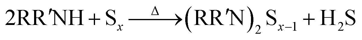
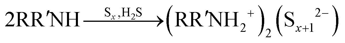
As shown in a reported article, sulfur exists as S8 rings in its standard state.25,26 At relatively low temperature (<50 °C) heating, the S8 rings are liable to open under attack by nitrogen from an alkylamine and form a N–S bond (reaction (1), R represents alkyl group). Secondary amines will react with sulfur to form two N–S bonds, resulting in liberation of H2S.27,28 In case of the S–Oam solution in this study, the polysulfide anions react with the remaining oleylammonium and liberate H2S, causing decreased stoichiometry of S in polysulfides (reaction (2)). Meanwhile, H2S is proposed to react with S8 to form Sx2− anions under the reducing effect of amino groups (reaction (3)).29 The reactions are presented as follows: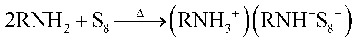 | (1) |
 | (2) |
 | (3) |
A schematic diagram of sulfurization treatment process on perovskite films is illustrated in Scheme 1. A certain volume of the as-prepared S–Oam solution (reaction (4)) was mixed with octadecene and preheated to 40 °C before use. Then, an annealed perovskite film was transferred to the S–Oam/octadecene solution and dipped for 3 minutes. During the dipping process, the perovskite surface was etched by S–Oam in solution, while octadecene, with the long carbon chains, serves as a stabilizer in the surface reaction.30 Under the etching effect of H2S, methylamine cations (MA+) and iodide anions (I−) are prone to dissolve into the solution, leading to degradation of the perovskite (reaction (5)). OP molecules were anchored on the perovskite film by interatomic interactions: nitrogen atoms in the Sx rings can form H-bonds with MA+, while sulfur atoms tend to form Pb–S bonds with Pb2+. Moreover, we measured the pH of S–Oam (pH = 11.7) and S-25 (pH = 7.9) solutions at 40 °C and observed that alkaline conditions favored the proceeding of reactions. It can be inferred that the S-25 treated film was formed by dynamic equilibrium between etching and assembling, thus greatly benefitting the device. As depicted in Scheme 1, the hydrophobic OPs layer protects the perovskite from being attacked by water molecules as well as prevents ion migration between perovskite/HTL interface, resulting in a stabilized perovskite film. Finally, the residual oleylamine, octadecene and other impurities can be successfully removed by rinsing with cyclohexane without affecting the OPs assembly on the perovskite film. Generation of OPs and decomposition of perovskite, induced by H2S, should proceed as per the following equations:
 | (4) |
 | (5) |
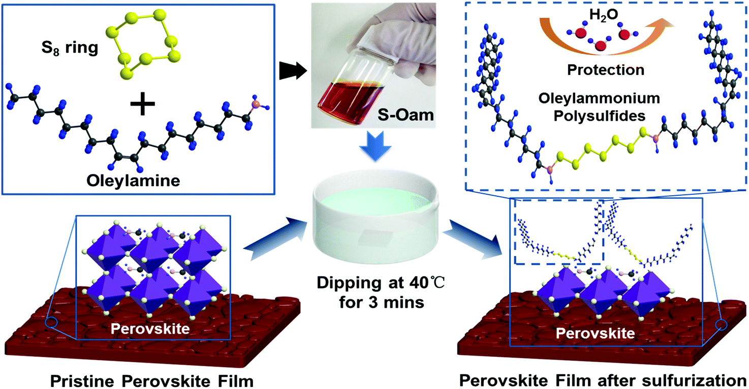 | ||
| Scheme 1 Schematic of the surface modification process with S–Oam solution by H2S etching and OPs assembling on the perovskite surface. Hydrophobic properties are attributed to the long carbon chains of OPs. (The blue, red, black, pink, gray and yellow balls represent hydrogen, oxygen, carbon, nitrogen, lead and sulfur atoms, respectively.) | ||
To confirm the existence of OPs and investigate their structure, two signals were alternatively pulsed to obtain their 1H-HCOSY 2D NMR spectra. As shown in the bitmap plots in Fig. 1(a and b), for both pristine and S-25 treated perovskite samples, protons of N–H and C–H in MA+ were observed at 7.46 ppm and 2.42 ppm, respectively, without drift.10 The bitmap plot of the sample after dipping treatment, however, shows several signal regions in a diagonal line. The chemical shifts of protons in imido, methylene adjacent to imido, middle alkenyl and terminated methyl were 1.50 ppm, 2.63 ppm, 5.34 ppm and 0.88 ppm, respectively. Other protons in the long carbon chain were distributed in 1.26–1.33 ppm range.23,31 Overall, it could be inferred that OP molecules were successfully assembled onto the perovskite film.
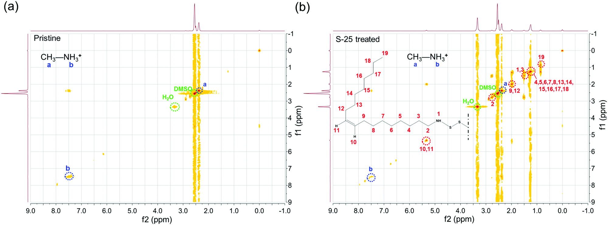 | ||
| Fig. 1 1H-HCOSY spectra of (a) pristine and (b) S-25 samples. The mechanically scraped perovskite powder was dissolved in deuterated dimethyl sulfoxide (DMSO-d6) before analysis. Chemical shifts of protons in methyl (a, blue letter) and amino (b, blue letter) for MA+ and part of the OPs molecule (number 1–19) are marked with blue dashed circle and red dashed circle, respectively. | ||
To further understand the etching behavior of an S–Oam solution, MAPbI3 films were coated on the FTO/TiO2 substrate via sequential deposition method, and then dipped in 25 μL of S–Oam solution. X-ray photoelectron spectra (XPS) were recorded to study the bond and valence information of S-25 treated sample. As shown in Fig. 2(a), a notable peak located at 160.2 eV for S 2p was found in the dip treated perovskite, which suggested the formation of S–Pb bond.32,33 In addition, a peak corresponding to the S–S bond in S8 ring was found at 164.4 eV.34 Another signal at 167.8 eV was supposed to be ascribed to the N–S bond.35 In comparison, no such S 2p signals were found in the XPS map of the pristine sample. Binding energies of C 1s for pristine and S-25 treated samples are illustrated in Fig. 2(b). Two peaks in the spectrum of the pristine sample, located at 286.2 eV and 284.8 eV, represent the C–N bond and C–C bond, respectively. After dipping treatment, the peak of C–N bond slightly shifted to a lower binding energy field by approximately 0.6 eV (285.6 eV). This variation manifests the change in chemical environment of the C–N bond from methylamine to oleylamine.36 From the rising intensity of C–C bond signal, we deduced that the compound loaded on the perovskite film was OPs. However, significant drop in intensities of Pb 4f, I 3d and N 1s peaks was found, as shown in Fig. S1 (ESI†). This can be explained by the coverage of long carbon chains on the perovskite, which weakened the signal response of noncarbon elements. Full XPS spectra are provided in Fig. S1 (ESI†). Furthermore, SEM-EDS mapping and ICP-AES spectra were recorded to detect S in the S-25 sample (Fig. S2 and Table S1, ESI†), the results of which were in line with XPS measurements.
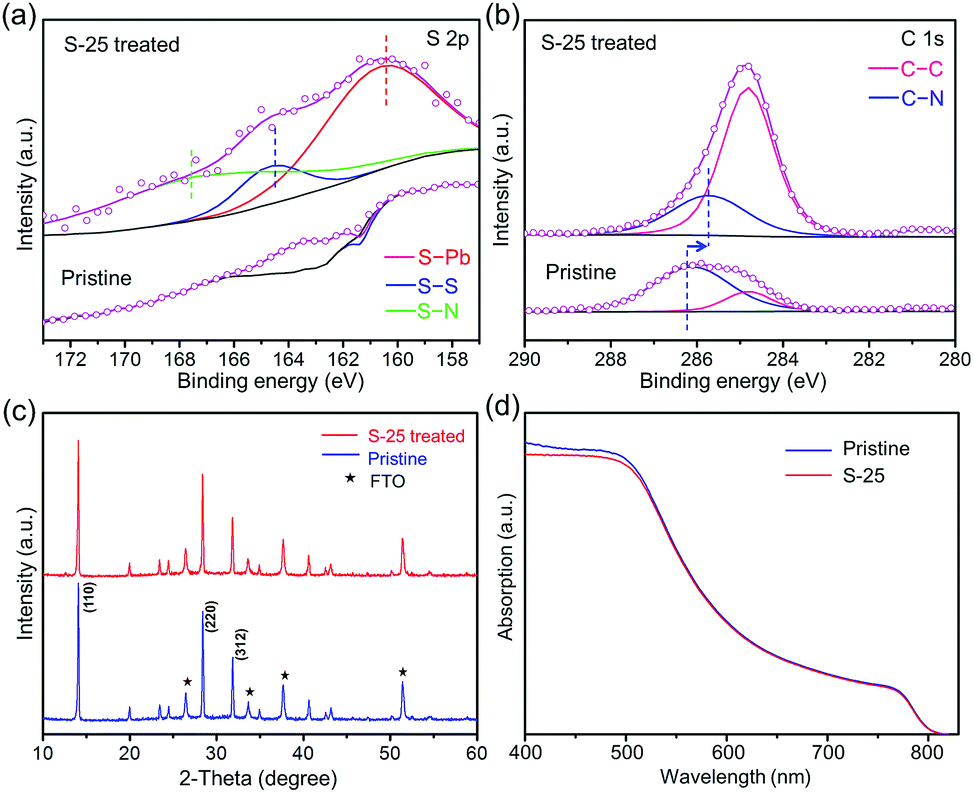 | ||
| Fig. 2 (a and b) XPS patterns of S 2p and C 1s of S-25 treated samples. (c) XRD patterns and (d) absorption spectra of pristine and S-25 samples. | ||
As presented in Fig. S3(a–f) (ESI†), we investigated the relationship between the as-prepared S–Oam solution volume and crystallization behavior of the perovskite films. As the volume of S–Oam increased from 0 to 150 μL, the color of the perovskite thin films gradually lightened and became transparent when the volume reached 150 μL. Moreover, scanning electron microscopy (SEM) images (Fig. S3(A–F), ESI†) suggest that bright spots and grain gap appear on the perovskite surface after S–Oam dipping treatment, forming a ravine-shaped morphology on the perovskite layer surface. With the increase in S–Oam solution volume, the grain gap enlarges and the grain size starts to decrease, which indicates a deeper etching degree of the perovskite film by S–Oam. As a result of continuous dissolution of perovskite into the solution, the entire perovskite layer is etched at high S–Oam concentration condition, thus changing the morphology of substrate (Fig. S3 (ESI†)). Furthermore, atomic force microscopy (AFM) images (Fig. S4(a and b), ESI†) were recorded to study the roughness of the perovskite films. The variation of mean roughness and maximum height in selected area for pristine (15.34 nm, 144.60 nm, respectively) and S-25 (11.74 nm, 137.85 nm, respectively) samples manifests that S–Oam can etch surface swelling and smoothen the film, leading to a better contact between the perovskite and HTL. As a control, the same volume of Oam was added to octadecene for dipping treatment. Only upon treatment with 150 μL of this solution, the color of perovskite film lightens and the grain gap enlarges (Fig. S5(a–d and A–D), ESI†), which suggests that the reaction product of sulfur and oleylamine accelerates the etching process.
X-ray diffraction (XRD) pattern (Fig. 2(c)) shows three distinct peaks appearing at 14.1°, 28.4° and 31.9°, which correspond to the (110), (220) and (312) crystal planes of pristine MAPbI3. The peak position and intensity of S-25 treated sample almost displayed no difference compared to those of the pristine sample. However, the peak intensity of perovskite started to decrease when the volume of S–Oam surpassed 50 μL (Fig. S6, ESI†). As depicted in the UV-vis spectra (Fig. 2(d)), the profile and slopes of absorption curves for pristine and S-25 samples nearly overlap, which indicates that the dipping treatment barely impacts optical absorption properties and band gap of the perovskite film.
To study the influence of dipping treatment on the performance of solar cells, a normal planar heterojunction configuration FTO/planar-TiO2/MAPbI3/spiro-OMeTAD/Ag was utilized (Fig. 3(a)). Band alignment of the as-fabricated device is presented in Fig. 3(b). To investigate the defects and carrier recombination in the perovskite film, we conducted steady-state photoluminescence (PL) test. As shown in Fig. 3(c), the PL intensity and peak area of S-25 sample is higher than those of the pristine sample when deposited on glass. In the absence of ETL, the PL intensity represents the fluorescence quenching intensity of bulk perovskite, which directly manifests the number of defects in the perovskite film. The enhancement in PL intensity can be attributed to retardation of the trap-related non-radiative recombination, induced by the pre-etching process.37,38 Thus, it is believed that the OPs layer can effectively passivate a perovskite film and reduce the number of defects.
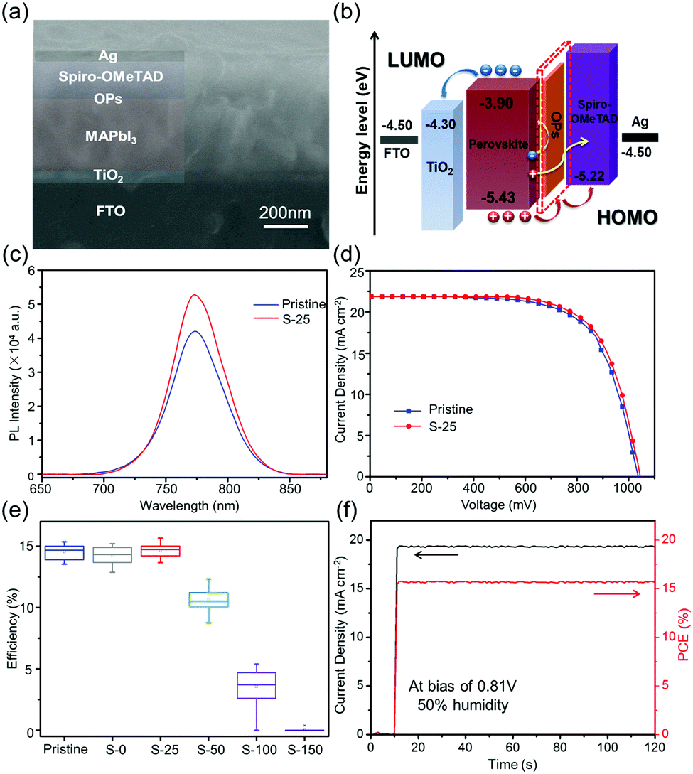 | ||
| Fig. 3 (a) Cross-sectional SEM image of sulfurized device with the FTO/TiO2/MAPbI3/OPs/HTL/Ag structure. (b) Energy level diagram of sulfurized perovskite device. (c) Steady-state photoluminescence spectra of pristine and S-25 samples. (d) J–V curves of pristine and S-25 devices. (e) Box-plot of PCEs for pristine, S-0, S-25, S-50, S-100 and S-150 devices. (f) Steady-state photocurrent and power output at MPP for the S-25 champion device. | ||
Photocurrent density–photovoltage (J–V) curves were measured from forward bias to short circuit under AM 1.5 standard illumination (100 mW cm−2) with a scan rate of 0.15 V s−1. We first investigated the variation in S–Oam volumes; 25 individual devices were selected for each volume. As shown in the Fig. 3(d), the S-25 treated device yields an open-circuit voltage (VOC) of 1.04 V, a fill factor (FF) of 0.69, and a PCE of 15.71%. For the same batch, the pristine device exhibits a VOC of 1.03 V, a FF of 0.68 and a PCE of 15.35%. Moreover, the Oam-25 treated device yielded a sharply reduced PCE of 0.72% (Fig. S7, ESI†). From the box-plot data (Fig. 3(e)) we know that the dipping treatment has minor impact on the performance of devices when the volume is below 25 μL as the surface morphology of such films is similar to the untreated perovskite film, according to SEM images. However, PCE values declined rapidly when the treatment volume surpassed 25 μL, which corresponds to the deeply etched morphology of perovskite films. Then, we selected the maximum efficiency-device of S-25 for comparison with the pristine device. Stable power output (SPO) test was conducted on S-25 treated device at bias of 0.81 V under a relative humidity of 50% condition (Fig. 3(f)). Performance at the maximum power point (MPP) is a vital factor to judge the stability of the device at high-load operation. As we desired, a stable photocurrent and efficiency output were obtained for S-25 treated device, with a constant illumination time of 120 s.
Long-term stability under high humidity conditions is always a big challenge for OHPSCs. We carried out humidity tests for pristine and S-25 treated devices under a relative humidity condition of 40 ± 10% in the temperature range of 25–35 °C. As shown in Fig. 4(a), the pristine device lost almost all efficiency by the 8th day, while the S-25 treated device still retains more than 70% of its initial PCE even after 14 days. In order to clearly present the variable photovoltaic performances of pristine and S-25 treated devices during this test, the observed trends of normalized VOC, JSC and FF are displayed in Fig. 4(b–d). Detailed performance values for the pristine and sulfurized devices are exhibited in Table S2 (ESI†). In addition, we performed water contact angle test on the pristine and S-25 treated perovskite films (Fig. 4(e)). The contact angles at 5 s were 52.65° and 83.35° for pristine and S-25 treated samples, respectively. Then, these angles changed to 34.87° and 59.64° after 10 min of droplet-loading, which suggests that dipping treatment endows the perovskite film with better hydrophobicity. Combining these results with the PCE test results, we demonstrated that the enhanced moisture tolerance of S-25 treated device is ascribed to the hydrophobic OPs layer assembled on the perovskite film. The bulky alkyl chains in OPs are in situ assembled by forming Pb–S and hydrogen bonds, which strengthen the OPs–perovskite interactions and prevent the perovskite from interacting with water molecules.
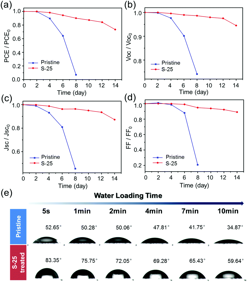 | ||
| Fig. 4 Long-term stability tests of pristine and S-25 solar cells in air for 14 days. The evolution (a–d) of normalized PCE, VOC, JSC and FF for pristine and sulfurized devices. (e) Photographs of water contact angles for pristine and S-25 samples. | ||
Conclusions
In summary, we utilized a facile and easily-controlled sulfurization of perovskite film, by dipping treatment with alkylammonium polysulfides and H2S in a S–Oam precursor. The assembled OPs act both as passivated and hydrophobic layers at the perovskite/HTL interface, which was formed by post-dipping reaction with dual-functional S–Oam solution. The device after surface modification exhibited a significantly enhanced moisture stability compared to the untreated device. This facile and low-cost solution processed method provides new insights into surface modification of perovskite solar cells to fabricate highly stable, efficient and reproducible devices.Conflicts of interest
There are no conflicts to declare.Acknowledgements
This study was financially supported by National Natural Science Foundation of China (51602103), National Natural Science Funds for Distinguished Young Scholar (51725201), Young Elite Scientists Sponsorship Program by CAST (2017QNRC001), Shanghai Pujiang Program (18PJD009), “Chen Guang” Project supported by Shanghai Municipal Education Commission and Shanghai Education Development Foundation (15CG26), Fundamental Research Funds for the Central Universities (222201718002), and the Major Research plan of National Natural Science Foundation of China (91534202).Notes and references
- A. Kojima, K. Teshima, Y. Shirai and T. Miyasaka, J. Am. Chem. Soc., 2009, 131, 6050–6051 CrossRef CAS PubMed.
- https://www.nrel.gov/pv/assets/images/efficiency-chart.png .
- A. M. A. Leguy, Y. Hu, M. Campoy-Quiles, M. I. Alonso, O. J. Weber, P. Azarhoosh, M. van Schilfgaarde, M. T. Weller, T. Bein, J. Nelson, P. Docampo and P. R. F. Barnes, Chem. Mater., 2015, 27, 3397–3407 CrossRef CAS.
- J. A. Christians, P. A. Miranda Herrera and P. V. Kamat, J. Am. Chem. Soc., 2015, 137, 1530–1538 CrossRef CAS PubMed.
- J. Liang, C. X. Wang, Y. R. Wang, Z. R. Xu, Z. P. Lu, Y. Ma, H. F. Zhu, Y. Hu, C. C. Xiao, X. Yi, G. Y. Zhu, H. L. Liu, L. B. Ma, T. Chen, Z. X. Tie, Z. Jin and J. Liu, J. Am. Chem. Soc., 2016, 138, 15829–15832 CrossRef CAS PubMed.
- Q. S. Shan, J. H. Li, J. Z. Song, Y. S. Zou, L. M. Xu, J. Xue, Y. H. Dong, C. X. Huo, J. W. Chen, B. N. Han and H. B. Zeng, J. Mater. Chem. C, 2017, 5, 4565–4570 RSC.
- Z. F. Shi, Y. Li, S. Li, X. J. Li, D. Wu, T. T. Xu, Y. T. Tian, Y. S. Chen, Y. T. Zhang, B. L. Zhang, C. X. Shan and G. T. Du, Adv. Funct. Mater., 2018, 28, 1707031 CrossRef.
- Z. F. Shi, S. Li, Y. Li, H. F. Ji, X. J. Li, D. Wu, T. T. Xu, Y. S. Chen, Y. T. Tian, Y. T. Zhang, C. X. Shan and G. T. Du, ACS Nano, 2018, 12, 1462–1472 CrossRef CAS PubMed.
- G. Li, T. Y. Zhang and Y. X. Zhao, J. Mater. Chem. A, 2015, 3, 19674–19678 RSC.
- S. Yang, Y. Wang, P. Liu, Y. B. Cheng, H. J. Zhao and H. G. Yang, Nat. Energy, 2016, 1, 15016–15022 CrossRef CAS.
- H. Tsai, W. Nie, J. C. Blancon, C. C. Stoumpos, R. Asadpour, B. Harutyunyan, A. J. Neukirch, R. Verduzco, J. J. Crochet, S. Tretiak, L. Pedesseau, J. Even, M. A. Alam, G. Gupta, J. Lou, P. M. Ajayan, M. J. Bedzyk, M. G. Kanatzidis and A. D. Mohite, Nature, 2016, 536, 312–318 CrossRef CAS PubMed.
- W. Li, C. Zhang, Y. Ma, C. Liu, J. Fan, Y. Mai and R. E. I. Schropp, Energy Environ. Sci., 2018, 11, 286–293 RSC.
- Y. Hou, X. Chen, S. Yang, C. Li, H. J. Zhao and H. G. Yang, Adv. Funct. Mater., 2017, 27, 1700878 CrossRef.
- Q. Liu, M. Qin, W. Ke, X. Zheng, Z. Chen, P. Qin, L. Xiong, J. Ma, Z. Zhang and G. Fang, Adv. Funct. Mater., 2016, 26, 6069–6075 CrossRef CAS.
- Y. Hou, X. Chen, S. Yang, Y. L. Zhong, C. Z. Li, H. J. Zhao and H. G. Yang, Nano Energy, 2017, 36, 102–109 CrossRef CAS.
- X. Li, J. Yang, Q. Jiang, H. Lai, S. Li, J. Xin, W. Chu and J. Hou, ACS Nano, 2018, 12, 5605–5614 CrossRef CAS PubMed.
- Q. Wang, Q. Dong, T. Li, A. Gruverman and J. Huang, Adv. Mater., 2016, 28, 6734–6739 CrossRef CAS PubMed.
- Y. Bai, Q. Dong, Y. Shao, Y. Deng, Q. Wang, L. Shen, D. Wang, W. Wei and J. Huang, Nat. Commun., 2016, 7, 12806–12814 CrossRef CAS PubMed.
- X. Li, M. I. Dar, C. Yi, J. Luo, M. Tschumi, S. M. Zakeeruddin, M. K. Nazeeruddin, H. Han and M. Grätzel, Nat. Chem., 2015, 7, 703–715 CrossRef CAS PubMed.
- I. Hwang, I. Jeong, J. Lee, M. J. Ko and K. Yong, ACS Appl. Mater. Interfaces, 2015, 7, 17330–17339 CrossRef CAS PubMed.
- L. Gao, S. Huang, L. Chen, X. Li, B. Ding, S. Huang and G. Yang, Sol. RRL, 2018, 2, 1800088 CrossRef.
- T. Y. Wen, S. Yang, P. F. Liu, L. J. Tang, H. W. Qiao, X. Chen, X. H. Yang, Y. Hou and H. G. Yang, Adv. Energy Mater., 2018, 8, 1703143 CrossRef.
- J. W. Thomson, K. Nagashima, P. M. Macdonald and G. A. Ozin, J. Am. Chem. Soc., 2011, 133, 5036–5041 CrossRef CAS PubMed.
- B. Yuan, X. Tian, S. Shaw, R. E. Petersen and L. Cademartiri, Phys. Status Solidi A, 2016, 214, 543–548 Search PubMed.
- L. Pauling, Proc. Natl. Acad. Sci. U. S. A., 1949, 35, 495–499 CrossRef CAS.
- S. S. Zumdahl, Chemical Principles, Houghton Mifflin, Boston, 2009 Search PubMed.
- T. G. Levi, Gazz. Chim. Ital., 1930, 60, 975–987 CAS.
- T. G. Levi, Gazz. Chim. Ital., 1931, 61, 286–293 CAS.
- R. E. Davis and H. F. Nakshbendi, J. Am. Chem. Soc., 1962, 84, 2085–2090 CrossRef CAS.
- M. V. Kovalenko, M. Scheele and D. V. Talapin, Science, 2009, 324, 1417–1420 CrossRef CAS PubMed.
- X. Liu, M. Atwater, J. H. Wang, Q. Dai, J. H. Zou, J. P. Brennan and Q. Huo, J. Nanosci. Nanotechnol., 2007, 7, 3126–3133 CrossRef CAS PubMed.
- D. S. Zingg and D. M. Hercules, J. Phys. Chem., 1978, 82, 1992–1995 CrossRef CAS.
- J. H. Heo, M. H. Jang, M. H. Lee, D. H. Shin, D. H. Kim, S. H. Moon, S. W. Kim, B. J. Park and S. H. Im, ACS Appl. Mater. Interfaces, 2017, 9, 41104–41110 CrossRef CAS PubMed.
- A. M. D. Jong, H. J. Borg, L. J. V. Ijzendoorn, V. G. F. M. Soudant, V. H. J. D. Beer, J. A. R. V. Veen and J. W. Niemantsverdriet, J. Phys. Chem., 1993, 97, 6477–6483 CrossRef.
- M. Doring, M. Rudolph and E. Uhlig, Z. Anorg. Allg. Chem., 1987, 554, 217–226 CrossRef.
- D. H. Karweik and N. Winograd, Inorg. Chem., 1976, 2336–2342 CrossRef CAS.
- C. Ding, Y. Zhang, F. Liu, Y. Kitabatake, S. Hayase, T. Toyoda, R. Wang, K. Yoshino, T. Minemoto and Q. Shen, Nanoscale Horiz., 2018, 3, 417–429 RSC.
- J. J. Shi, H. Y. Zhang, Y. M. Li, J. J. Jasieniak, Y. S. Li, H. J. Wu, Y. H. Luo, D. M. Li and Q. B. Meng, Energy Environ. Sci., 2018, 11, 1460–1469 RSC.
Footnotes |
| † Electronic supplementary information (ESI) available: Experimental procedures, characterization data. See DOI: 10.1039/c8nh00163d |
| ‡ These authors contributed to this article equally. |
| This journal is © The Royal Society of Chemistry 2019 |