
Enhancing potassium-ion battery performance by defect and interlayer engineering†
Yang
Xu‡
 *a,
Farzaneh
Bahmani‡
ab,
Min
Zhou
a,
Yueliang
Li
c,
Chenglin
Zhang
a,
Feng
Liang
d,
Sayed Habib
Kazemi
b,
Ute
Kaiser
c,
Guowen
Meng
*e and
Yong
Lei
*a
*a,
Farzaneh
Bahmani‡
ab,
Min
Zhou
a,
Yueliang
Li
c,
Chenglin
Zhang
a,
Feng
Liang
d,
Sayed Habib
Kazemi
b,
Ute
Kaiser
c,
Guowen
Meng
*e and
Yong
Lei
*a
aFachgebiet Angewandte Nanophysik, Institut für Physik & ZMN MacroNano (ZIK), Technische Universität Ilmenau, Ilmenau 98693, Germany. E-mail: yang.xu@tu-ilmenau.de; yong.lei@tu-ilmenau.de
bDepartment of Chemistry, Institute for Advanced Studies in Basic Sciences, Zanjan 45137, Iran
cCentral Facility for Electron Microscopy, Electron Microscopy Group of Materials Science, Ulm University, Ulm 89081, Germany
dState Key Laboratory of Complex Nonferrous Metal Resources Clean Utilization, Kunming University of Science and Technology, Kunming 650093, China
eInstitute of Solid State Physics, Chinese Academy of Sciences, Hefei, Anhui 230031, China. E-mail: gwmeng@issp.ac.cn
First published on 9th October 2018
Abstract
Defect and interlayer engineering is applied to exploit the large van der Waals gaps of transition metal dichalcogenides for potassium-ion batteries (KIBs). As a demonstrator, MoS2 nanoflowers with expanded interlayer spacing and defects in the basal planes are used as KIB anodes in the voltage range of 0.5–2.5 V, where an intercalation reaction rather than a conversion reaction takes place to store K-ions in the van der Waals gaps. The nanoflowers show enhanced K-storage performance compared to the defect-free counterpart that has a pristine interlayer spacing. Kinetic analysis verifies that the K-ion diffusion coefficient and surface charge storage are both enhanced in the applied voltage range of the intercalation reaction. The collective effects of expanded interlayer spacing and additionally exposed edges induced by the in-plane defects enable facile K-ion intercalation, rapid K-ion transport and promoted surface K-ion adsorption simultaneously.
Conceptual insightsThe large size of K-ions causes kinetic difficulties in potassium-ion batteries. Two-dimensional transition metal dichalcogenides (2D TMDs) have come into the spotlight owing to the unique van der Waals gaps that form ideal 2D K-ion diffusion pathways. Previous work was focused on pursuing high capacity through the reduction reaction and therefore lacks the exploitation of the van der Waals gaps as a natural asset to store K-ions, not to mention that the reaction could destroy the gaps. We propose a concept of defect and interlayer engineering to fully exploit the van der Waals gaps for K-ion storage. The engineering creates in-basal-plane defects that generate extra sites to intercalate K-ions and exposed edges to adsorb K-ions. It also expands the interlayer spacing to reduce K-ion diffusion resistance. As a proof-of-concept, MoS2 with an expanded interlayer spacing of 0.91 nm and defects in its basal planes exhibited 40% higher reversible capacity and 120% higher rate capability than the defect-free counterpart, in a controlled voltage window of intercalation reactions. The presented concept enhances K-ion intercalation, transportation and adsorption simultaneously, and transforms K-ion storage in TMDs from 2D to 3D. This work may provide insights into nanomaterial design using defects and ion storage in other (electro)chemical systems. |
Introduction
The greater abundance and accessibility of the Na and K resources compared with the Li resource have prompted researchers to investigate the feasibility of Na-ion and K-ion batteries (KIBs).1–5 Given the more negative redox potential of K+ than Na+ (K+/K = −2.93 V, Na+/Na = −2.71 V vs. standard hydrogen electrode), there could be no loss of cell capacity and energy density even though K+ is bigger than Na+,6 making KIBs hold much promise for large-scale stationary energy storage. However, the size of K+ imposes a major challenge to ion diffusion, often resulting in poor kinetics. This calls for electrode materials with proper structural features that could facilitate K-ion diffusion.Two-dimensional transition metal dichalcogenides (2D TMDs) have gained world-wide attention in recent years and are being heavily studied in many research domains.7–10 TMDs possess a unique layered structure characterized by the weak van der Waals interaction between neighboring layers and strong in-plane covalent bonding within each layer. Such uniqueness allows the intercalation of guest species in the interlayer space without significant structural distortion. In this regard, 2D TMDs have been employed as electrode materials in KIBs very recently.11–13 Hierarchical VS2 nanosheet assemblies12 and MoS2 “nano-rose”@reduced graphene oxide composites13 displayed some of the best electrochemical performances to date as KIB anodes owing to the architectural and/or compositional features. As we pointed out, the large van der Waals gaps should be ideal for fast 2D K-ion diffusion, but they have not been well exploited because these studies on KIBs focused on high capacity derived from the four-electron reduction reaction that could destroy the gaps as diffusion pathways. Wu et al. observed a stoichiometric K+ intercalation compound, K0.4MoS2, in commercial MoS2 power, and demonstrated a cycling stability under this intercalation ratio at the discharge depth of 0.5 V (vs. K+/K) to ensure the preservation of the van der Waals gaps.11 Despite the relatively low reversible capacity (∼64 mA h g−1) and moderate rate capability (∼55 mA h g−1 at 160 mA g−1), this work encourages us to fully exploit the van der Waals gaps for K-storage.
The enhancement of K-storage in the van der Waals gaps arises when two criteria are met (Fig. 1): (i) the interlayer spacing is expanded and (ii) the interlayer space becomes more accessible for K-ions to intercalate. On the one hand, interlayer expansion could straightforwardly facilitate K-ion transport because of the reduced transport resistance. On the other hand, making interlayer space more accessible could be achieved by creating defects in the basal planes of the layers, where micro-channels are created to act as K-ion intercalation sites to shorten the diffusion distance and open up the inner space between the layers. Moreover, the second point could bring extra benefit that the micro-channels could generate additional edges of the layers with additionally exposed edge sites that are known to exhibit a fast response to faradaic and non-faradaic processes.14 Surface K-ion storage and fast kinetics can be expected since edge sites are theoretically and experimentally found to be active for the bonding interaction with ions and molecules.15–17 Surprisingly, utilization of the edge sites of TMDs is scarce in the studies of ion batteries. It is therefore of great importance to achieve a full exploitation of the van der Waals gaps in 2D TMDs by realizing the above discussed benefits, yet it remains challenging to simultaneously expand interlayer spacing, open interlayer space, and create additional edge sites. This shall lead to the enhancement of K-storage in 2D TMDs.
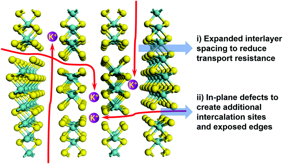 | ||
| Fig. 1 Illustration of defect and interlayer engineering to enhance KIB performance. | ||
Herein, we highlight a facile defect and interlayer engineering to meet the challenge. We chose MoS2 as a demonstrator because it has received rapidly increasing attention as a KIB anode material. We obtained interlayer-expanded and defect-rich MoS2 nanoflowers (D-MoS2 NFs) by adjusting the ratio between the Mo and S precursors during synthesis. By controlling the working voltage to be 0.5–2.5 V in which the intercalation reaction dominates the electrochemical mechanism, we demonstrate the feasibility of enhancing KIB performance through modulating K-storage behavior in the van der Waals gaps. The nanoflowers exhibited a K-intercalation capacity that is 40% higher than that of the defect-free counterpart with pristine interlayer spacing, and a rate capability of ∼50 mA h g−1 at 0.8 A g−1. We attribute the enhancement to the increased K-ion diffusivity and surface charge storage, which is enabled by the expanded interlayer spacing and in-plane defects.
Results and discussion
D-MoS2 NFs were synthesized by reacting ammonium molybdate with excess thiourea through a one-pot hydrothermal reaction, while the defect-free NFs were obtained using the stoichiometric ratio (ESI†). The excess thiourea releases a large amount of ammonia that can be in situ intercalated into the space between the MoS2 layers, which is responsible for the expansion of the interlayer spacing. A similar phenomenon was observed in previous work of transition metal dichalcogenides with expanded interlayer spacing.18,19 The morphology and the microstructure of the as-prepared samples were characterized via scanning electron microscopy (SEM) and aberration-corrected transmission electron microscopy (TEM). Fig. S1a and c (ESI†) show that both samples have a flower-like spherical architecture with a diameter of 2.5–3.5 μm. Fig. S1b and d (ESI†) reveal that the flowers consist of ultrathin nanosheets with obvious corrugations. The thickness of the nanosheets is estimated to be around 10 nm. High-resolution TEM (HRTEM) images in Fig. 2 give direct depiction of the side and basal planes, showing a typical lamellar structure with curvy edges and a thickness of around 10 nm, which is consistent with the SEM observations. An interlayer spacing of 0.91 nm was observed in D-MoS2 NFs (Fig. 2a), while 0.63 nm was observed in MoS2 NFs (Fig. 2c), demonstrating a substantial expansion of the interlayer space. The crystal fringes of D-MoS2 are discontinuous along the curvy edge, forming “cracks” at different locations indicated by the arrows, which is attributed to the rich defects in basal planes.20,21 A lattice fringe of 0.27 nm, corresponding to the d spacing of the (100) plane of MoS2, can be seen in the basal planes of both samples (Fig. 2b and d), suggesting the same atomic orientation along this dimension. However, careful observation reveals that the directions of the (100) fringes of D-MoS2 NFs are not consistent over the entire basal surface and slightly rotate from one micro-region to another (Fig. 2b), causing lattice fringe distortion as indicated by the circles. The generated defects in the basal planes can cause discontinuity of the sides and additionally exposed edges (“cracks” in Fig. 2a).17,22 In contrast, more continuous and highly oriented fringes are found in MoS2 NFs (Fig. 2d). Three-window elemental maps (Fig. S2, ESI†) acquired through energy-filtered TEM (EFTEM)23,24 demonstrate the existence and even distribution of Mo and S in both samples.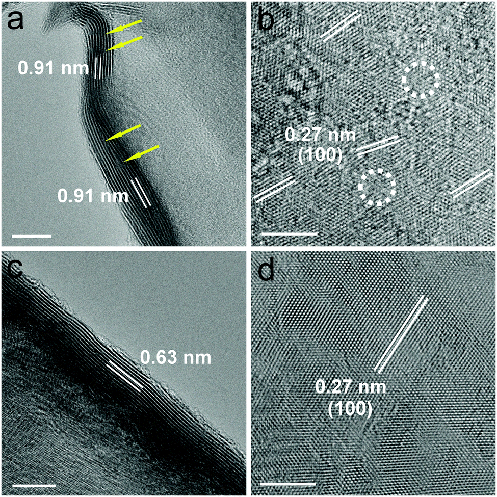 | ||
| Fig. 2 HRTEM images of the side (a and c) and basal planes (b and d) of D-MoS2 (a and b) and MoS2 NFs (c and d). The “cracks” indicated by the arrows in (a) show the discontinuity of the side, implying the rich defects caused by the missing atoms. Scale bars: 10 nm (a and c) and 5 nm (b and d). | ||
Fig. 3a shows the X-ray diffraction (XRD) patterns that can be well indexed to hexagonal MoS2 (JCPDS 37-1492). Peak broadening implies a small number of stacked layers as observed in Fig. 2a and c. A shift of the (002) peak from 14.4° in the standard pattern to 14.0° in the experimental patterns indicates an increased interlayer spacing to 0.63 nm, which agrees with other reported nanosized MoS2.25,26 D-MoS2 NFs show another peak located at 9.7° that corresponds to the substantially expanded interlayer spacing of 0.91 nm that is observed in Fig. 2a. A second-order (004) diffraction peak appears between 17° and 19°, which could probably be ascribed to ammonia intercalating in the interlayer space.18,27 After being annealed at 700 °C, the absence of both peaks indicates that ammonia is expelled from the interlayer space, resulting in the conversion to the thermodynamically stable structure and the restoration to the spacing of 0.63 nm (Fig. S3, ESI†). This provides an auxiliary support of the expanded spacing under the as-prepared conditions.20 Two broadened peaks at 32° and 57° can be indexed to (100) and (110) planes of MoS2, respectively, once again indicating that the two samples have the same atomic orientation along the basal planes. It is worth noting that D-MoS2 exhibits more broadened (100) and (110) peaks than MoS2, which is attributed to the more disordered crystal structure caused by the in-plane defects, as seen in Fig. 2b where the defects induce many nanodomains in the basal planes. Raman spectra (Fig. 3b) show the peaks located at 381.6 and 407.1 cm−1 which are attributed to the planar (E12g) and out-of-plane (A1g) vibration modes of MoS2, respectively,13,28 further demonstrating the phase purity of the samples. As shown in the spectra of the X-ray photoelectron spectroscopy image (XPS, Fig. 3c and d), the peaks at 228.5 and 231.7 eV are assigned to Mo 3d5/2 and 3d3/2 of Mo4+, respectively, and those at 161.3 and 162.5 eV are assigned to S 2p3/2 and 2p1/2 of S2−, respectively. The lowered binding energies of 0.4–0.5 eV in D-MoS2 NFs imply their enlarged interlayer spacing.29 The atomic ratio of S![[thin space (1/6-em)]](https://www.rsc.org/images/entities/char_2009.gif) :Mo is 1.89 and 1.77 for D-MoS2 and MoS2 NFs, respectively. Previous studies reported that a metal edge with an unsaturated S coverage is the most stable structure among differently exposed edges, which results in a higher content of S.30 The obtained ratio hints that D-MoS2 NFs have more exposed Mo–S edges caused by the defects in basal planes. The combined analysis of the phase, composition, morphology and microstructure prove the existence of expanded interlayer spacing and defects along with the additionally exposed edges in D-MoS2 NFs. These features are expected to facilitate K-ion intercalation/diffusion and increase surface K-ion adsorption, leading to the enhancement of K-storage in the van der Waals gaps.
:Mo is 1.89 and 1.77 for D-MoS2 and MoS2 NFs, respectively. Previous studies reported that a metal edge with an unsaturated S coverage is the most stable structure among differently exposed edges, which results in a higher content of S.30 The obtained ratio hints that D-MoS2 NFs have more exposed Mo–S edges caused by the defects in basal planes. The combined analysis of the phase, composition, morphology and microstructure prove the existence of expanded interlayer spacing and defects along with the additionally exposed edges in D-MoS2 NFs. These features are expected to facilitate K-ion intercalation/diffusion and increase surface K-ion adsorption, leading to the enhancement of K-storage in the van der Waals gaps.
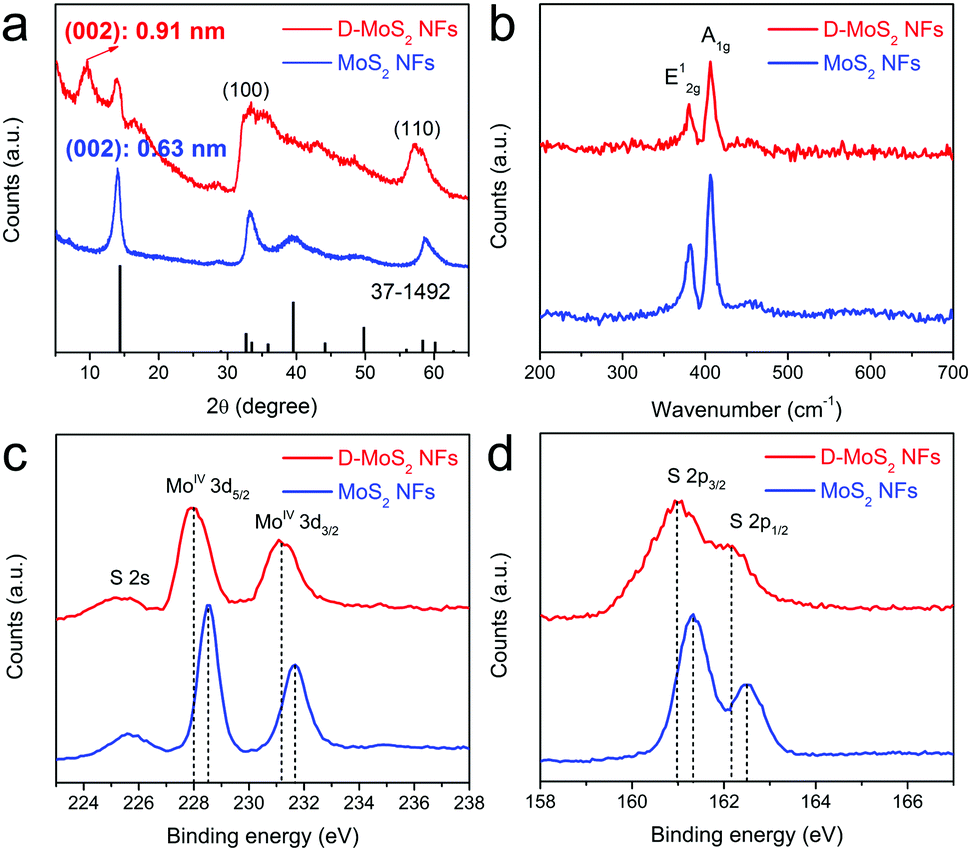 | ||
| Fig. 3 XRD patterns (a), Raman spectra (b), Mo 3d XPS spectra (c), and S 2p XPS spectra (d) of D-MoS2 and MoS2 NFs. | ||
Prior to testing batteries, it is critical to ensure that no crystal reconstruction caused by conversion reactions occurs upon K-ion intercalation/de-intercalation because reconstruction could destroy the van der Waals gaps as K-ion diffusion pathway. Previous studies showed that Na intercalation in MoS2 occurs at a voltage above 0.4 V (vs. Na+/Na), beyond which intercalation is replaced by conversion and the layered structure collapses.25,31,32 A recent work of KIBs showed 0.5 V (vs. K+/K) to be a suitable discharge depth at which only intercalation occurs.11 Accordingly, we chose a voltage range of 0.5–2.5 V in this work. Fig. 4 shows the XRD patterns of the two samples recorded after the first discharge and charge processes. All the patterns show the characteristic (002), (100), and (110) peaks of the layered structure, and no peaks of Mo or K2S were detected. The peak located at 9.7° remains upon cycling D-MoS2 NFs. The results prove that only intercalation reaction occurs and both samples maintain the layered structure.
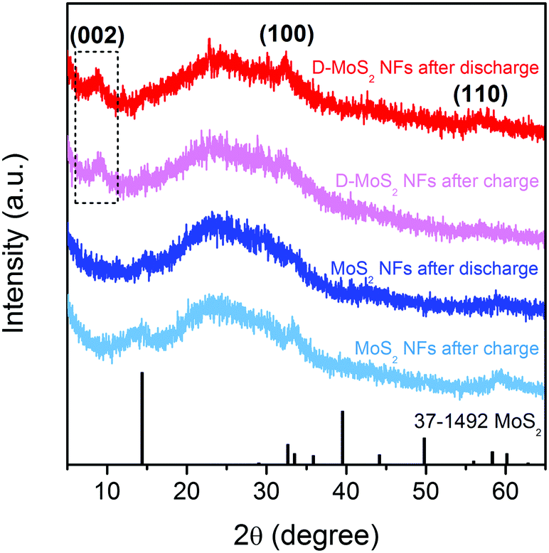 | ||
| Fig. 4 XRD patterns of D-MoS2 and MoS2 NFs after discharge and charge at the current density of 50 mA g−1. The broad peak between 20° and 30° is attributed to super P which is used as a conductive additive in the electrodes. | ||
With the above prerequisite established, we tested batteries to verify the defect and interlayer engineering for fully exploiting the van der Waals gaps towards enhanced KIB performance. Fig. S4 (ESI†) and Fig. 5a show the discharge–charge profiles at cycle 1, 2 and 100. MoS2 NFs have an initial discharge plateau at around 1.15 V, followed by a quasi-plateau centered at 0.75 V before reaching the cutoff voltage. At cycle 2, the discharge plateau shifts to a slightly higher voltage and becomes less defined, while the charge curve remains unchanged. For the case of D-MoS2, a slope replaces the plateau during discharge at cycle 1 and remains at cycle 2. Both samples display sloping curves at cycle 100 (Fig. 5a). The observed results agree with the cyclic voltammetry (CV) profiles shown in Fig. S5 (ESI†). The cycle 1 discharge/charge capacities are 280/104 mA h g−1 for D-MoS2 NFs and 225/77 mA h g−1 for MoS2 NFs, giving relatively low initial coulombic efficiencies (CEs) of 37 and 34%, respectively. This is most likely due to the decomposition of the electrolyte and the formation of the solid–electrolyte interface (SEI). We tested a control battery using only the conductive additive and the binder, and it showed a lower initial CE of 16% (Fig. S6, ESI†). As shown in Fig. 5b, the CE of D-MoS2 NFs reaches 90% at cycle 4, compared with cycle 7 for MoS2 NFs. D-MoS2 NFs delivered a reversible capacity of 94 mA h g−1 at cycle 100, being 40% higher than that of MoS2 NFs (67 mA h g−1). To the best of our knowledge, the presented K-intercalation capacity is higher than the previously reported numbers of MoS2 in KIBs and even comparable to some Na-intercalation capacities.11,25,31,33 The results show the necessity to control the electrochemical mechanism to be dominated by intercalation reactions in order to make full use of the van der Waals gaps. Rate performance is shown in Fig. 5c. D-MoS2 NFs exhibited higher capacities than MoS2 NFs at all testing rates. They delivered reversible capacities of 90, 75, 61, and 48 mA h g−1 at 100, 200, 400, and 800 mA g−1 (at cycle 13, 18, 23, and 28), in comparison with 65, 47, 33, and 22 mA h g−1 of MoS2 NFs at the corresponding rates. The capacity of D-MoS2 NFs was fully recovered to 104 mA h g−1 when the current density was reduced back to 50 mA g−1. Stable discharge–charge profiles of D-MoS2 NFs were obtained at all rates (Fig. 5d). The results show the benefits of the defect and interlayer engineering in MoS2. First, the expanded interlayer spacing kinetically facilitates the K-intercalation into and K-diffusion within the van der Waals gaps. The “cracks” provide additional ion intercalation sites, as D-MoS2 NFs show smaller discharge/charge polarization than MoS2 NFs in the prolonged cycles. The faster increased CE of D-MoS2 NFs during the initial cycles signals a higher reversibility owing to the less trapped K-ions between the layers.34,35 Second, the additionally exposed edges provide extra active sites to adsorb K-ions and increase surface charge storage. It can be evidenced by the more sloping voltage profiles of D-MoS2 NFs, which may originate from a distribution of adsorption energy.36,37
 | ||
| Fig. 5 (a) Discharge–charge profiles at cycle 2 and cycle 100. (b) Cycling performance. (c) Rate capability. (d) Discharge–charge profiles of D-MoS2 NFs at various current densities. | ||
We next sought to understand the defect and interlayer engineering by using two electrochemical characterization techniques. The first one is galvanostatic intermittent titration (GITT) that can evaluate the K-ion diffusion coefficient (Dk) during potassiation. Fig. 6a shows the potential response, where the potential change during each relaxation period represents the overpotential at the corresponding potassiation stage.38 D-MoS2 NFs exhibited much smaller overpotentials than MoS2 NFs in the entire potential range, which implies a better kinetic property. The linearity of the potential change with the square root of the relaxation time is shown in Fig. S7 (ESI†) and the calculation of Dk is shown in Fig. S8 (ESI†). Fig. 5b shows the values of Dk as a function of potential. Both samples displayed a progressively decreasing Dk with the potassiation proceeding toward the cut-off voltage, which agrees with the previous literature.39,40 However, the Dk of D-MoS2 NFs is much higher than that of MoS2 NFs, especially in the low-voltage region, being in accordance with the smaller overpotentials. This indicates that K-diffusion is much faster in D-MoS2 NFs owing to the expanded interlayer spacing and additional intercalation sites through the “cracks” that make interlayer spaces easily accessible for K-ions. The second characterization technique is CV. Fig. 6c and Fig. S9 (ESI†) show the curves of D-MoS2 and MoS2 NFs recorded at the scan rates of 0.1–1 mV s−1, respectively. For the case of D-MoS2 NFs, broad (de)potassiation peaks are maintained at high scan rates, and the peak separation hardly changes, signaling a very small polarization. For the case of MoS2 NFs, the peaks become steeper and large polarization can be seen. These observations once again indicate the better kinetic property of D-MoS2 NFs. We used the relationship of peak current (i) and scan rate (ν) to analyze the charge storage process according to the equation of i = aνb, where the b value can be extracted from the slope by plotting log(i) against log(ν). It is 0.5 for an ideal faradiac intercalation process controlled by semi-infinite linear diffusion while close to 1 for a surface charge storage process free of diffusion control.41,42 A good linear relationship can be seen in both samples (Fig. 6d). D-MoS2 NFs show the b values of 0.94 and 0.86 for the anodic and cathodic processes, respectively, and both are higher than those of MoS2 NFs (0.74 and 0.76). The comparison suggests that the K-storage is less diffusion controlled in D-MoS2 NFs, which can be ascribed to the active sites that could adsorb more K-ions on the additionally exposed edges, resulting in faster kinetics.
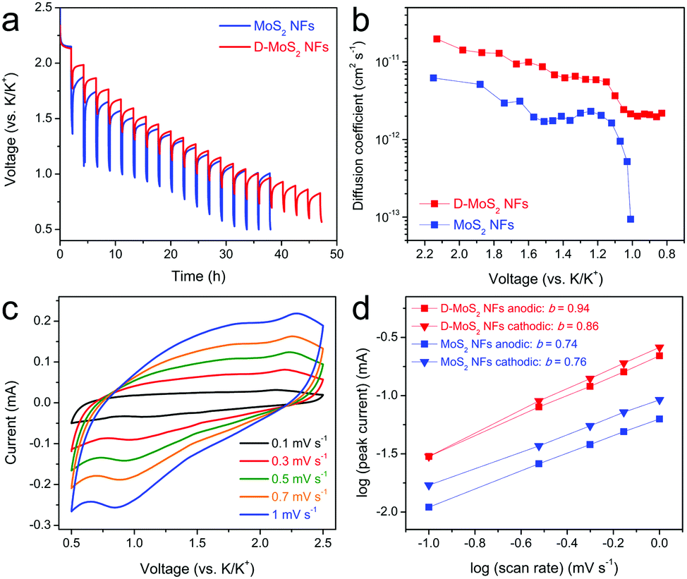 | ||
| Fig. 6 (a) GITT profiles of the discharge process. (b) Dk as a function of the state of the discharge process. (c) CV curves of D-MoS2 NFs at various scan rates. (d) b-value determination. | ||
Therefore, our electrochemical characterizations demonstrate that the kinetic property of MoS2 can be greatly improved by the expansion of interlayer spacing and exposure of additional edges. The presented material engineering not only facilitates K-intercalation and diffusion but also promotes surface K-storage, leading to the full exploitation of the van der Waals gaps.
We further characterized the morphology and the structure of the samples after 100 cycles. The nanosheet morphology can be seen (Fig. S10a and b, ESI†), despite the contour of the sheets being less defined due to the SEI layer. The preservation of the sheet-like shape indicates that the (de)intercalation process shows minimal damage to the microstructures of the MoS2 NFs, once again suggesting the preservation of the van der Waals gaps. HRTEM images (Fig. S10c and d, ESI†) show that both samples have more expanded layers compared with their original states, but the layers arrange more ordered in D-MoS2 NFs than in MoS2 NFs, which can be attributed to the better K-diffusion kinetics in the former. Nevertheless, the layered structure was kept intact with the cut-off voltage of 0.5 V, demonstrating a high structural reversibility during K-storage. It is very different from the conversion mechanism that has been popularly employed for ion-storage in MoS2, with a cut-off voltage of 0.1 V or lower, to reach a high capacity. The generation of Mo and metal sulfide destroys the layered structure and rebuilding the structure is difficult to be reversible, as evidenced by the detection of the Mo and sulfide phases after the charging process.43,44 The destruction of the layered structure often leads to a severe capacity decay, thus incorporation of the structure support and conductivity enhancers, e.g. carbon materials, was involved in almost all the previous literature of MoS2.13,45–48 Our work supports defect engineering as a new perspective to balance capacity and structural stability when designing electrode materials for KIBs.
Conclusions
In summary, taking MoS2 nanoflowers as an example, we demonstrate the crucial role of defect and interlayer engineering in 2D TMDs for exploiting the van der Waals gaps and enhancing KIB performance. The presented engineering creates expanded interlayer spacing and in-plane defects that lead to the exposure of additional edges of MoS2. As a result, facile K-ion intercalation, rapid K-ion transport and promoted surface K-ion storage are obtained simultaneously. The benefits were verified by a series of measurements, including long-term cycling, rate capability, GITT, and CV. The success of applying defect and interlayer engineering may pave the way towards a more efficient utilization of the prominent structural features of electrode materials, e.g., 2D diffusion pathways and lamellar structures. Significant improvement of KIBs can be expected by designing materials with defect-rich structures, and it may open new possibilities of using defects in other energy storage systems.Conflicts of interest
There are no conflicts to declare.Acknowledgements
This work was financially supported by the European Research Council (ThreeDsurface, 240144, and HiNaPc, 737616), BMBF (ZIK-3DNanoDevice, 03Z1MN11), and the German Research Foundation (DFG: LE 2249/4-1 and LE 2249/5-1).References
- N. Yabuuchi, K. Kubota, M. Dahbi and S. Komaba, Chem. Rev., 2014, 114, 11636–11682 CrossRef CAS PubMed.
- Y. Xu, M. Zhou and Y. Lei, Adv. Energy Mater., 2016, 6, 1502514 CrossRef.
- Y. Xu, M. Zhou and Y. Lei, Mater. Today, 2018, 21, 60–78 CrossRef CAS.
- J. C. Pramudita, D. Sehrawat, D. Goonetilleke and N. Sharma, Adv. Energy Mater., 2017, 7, 1602911 CrossRef.
- L. Wen, Z. Wang, Y. Mi, R. Xu, S. Yu and Y. Lei, Small, 2015, 11, 3408–3428 CrossRef CAS PubMed.
- L. Xue, H. Gao, W. Zhou, S. Xin, K. Park, Y. Li and J. B. Goodenough, Adv. Mater., 2016, 28, 9608–9612 CrossRef CAS PubMed.
- S. Manzeli, D. Ovchinnikov, D. Pasquier, O. V. Yazyev and A. Kis, Nat. Rev. Mater., 2017, 2, 17033 CrossRef CAS.
- X. Chia, A. Y. S. Eng, A. Ambrosi, S. M. Tan and M. Pumera, Chem. Rev., 2015, 115, 11941–11966 CrossRef CAS PubMed.
- J. Xu, J. Zhang, W. Zhang and C. S. Lee, Adv. Energy Mater., 2017, 7, 1700571 CrossRef.
- H. Zhu, C. Xiao, H. Cheng, F. Grote, X. Zhang, T. Yao, Z. Li, C. Wang, S. Wei, Y. Lei and Y. Xie, Nat. Commun., 2014, 5, 3960 CrossRef CAS PubMed.
- X. Ren, Q. Zhao, W. D. McCulloch and Y. Wu, Nano Res., 2017, 10, 1313–1321 CrossRef CAS.
- J. Zhou, L. Wang, M. Yang, J. Wu, F. Chen, W. Huang, N. Han, H. Ye, F. Zhao and Y. Li, Adv. Mater., 2017, 29, 1702061 CrossRef PubMed.
- K. Xie, K. Yuan, X. Li, W. Lu, C. Shen, C. Liang, R. Vajtai, P. Ajayan and B. Wei, Small, 2017, 13, 1701471 CrossRef PubMed.
- R. L. McCreery, Chem. Rev., 2008, 108, 2646–2687 CrossRef CAS PubMed.
- Y. Li, D. Wu, Z. Zhou, C. R. Cabrera and Z. Chen, J. Phys. Chem. Lett., 2012, 3, 2221–2227 CrossRef CAS PubMed.
- H. He, J. Lin, W. Fu, X. Wang, H. Wang, Q. Zeng, Q. Gu, Y. Li, C. Yan and B. K. Tay, Adv. Energy Mater., 2016, 6, 1600464 CrossRef.
- G. Ye, Y. Gong, J. Lin, B. Li, Y. He, S. T. Pantelides, W. Zhou, R. Vajtai and P. M. Ajayan, Nano Lett., 2016, 16, 1097–1103 CrossRef CAS PubMed.
- Q. Liu, X. Li, Z. Xiao, Y. Zhou, H. Chen, A. Khalil, T. Xiang, J. Xu, W. Chu, X. Wu, J. Yang, C. Wang, Y. Xiong, C. Jin, P. M. Ajayan and L. Song, Adv. Mater., 2015, 27, 4837–4844 CrossRef CAS PubMed.
- M. Gao, M. K. Y. Chen and Y. Sun, Nat. Commun., 2015, 6, 7493 CrossRef PubMed.
- J. Xie, J. Zhang, S. Li, F. Grote, X. Zhang, H. Zhang, R. Wang, Y. Lei, B. Pan and Y. Xie, J. Am. Chem. Soc., 2013, 135, 17881–17888 CrossRef CAS PubMed.
- S. Zhang, X. Yu, H. Yu, Y. Chen, P. Gao, C. Li and C. Zhu, ACS Appl. Mater. Interfaces, 2014, 6, 21880–21885 CrossRef CAS PubMed.
- J. Xie, H. Zhang, S. Li, R. Wang, X. Sun, M. Zhou, J. Zhou, X. W. D. Lou and Y. Xie, Adv. Mater., 2013, 25, 5807–5813 CrossRef CAS PubMed.
- C. Jeanguillaume, P. Trebbia and C. Colliex, Ultramicroscopy, 1978, 3, 237–242 CrossRef CAS PubMed.
- R. F. Egerton, Electron Energy-Loss Spectroscopy in the Electron Microscopy, Plenum Press, New York, 1996 Search PubMed.
- J. B. Cook, H. S. Kim, Y. Yan, J. S. Ko, S. Robbennolt, B. Dunn and S. H. Tolbert, Adv. Energy Mater., 2016, 6, 1501937 CrossRef.
- X. Wang, X. Shen, Z. Wang, R. Yu and L. Chen, ACS Nano, 2014, 8, 11394–11400 CrossRef CAS PubMed.
- Y. Xu, L. Wang, X. Liu, S. Zhang, C. Liu, D. Yan, Y. Zeng, Y. Pei, Y. Liu and S. Luo, J. Mater. Chem. A, 2016, 4, 16524–16530 RSC.
- T. S. Sahu and S. Mitra, Sci. Rep., 2015, 5, 12571 CrossRef CAS PubMed.
- X. Wang, Z. Guan, Y. Li, Z. Wang and L. Chen, Nanoscale, 2015, 7, 637–641 RSC.
- D. Chao, P. Liang, Z. Chen, L. Bai, H. Shen, X. Liu, X. Xia, Y. Zhao, S. V. Savilov and J. Lin, ACS Nano, 2016, 10, 10211–10219 CrossRef CAS PubMed.
- J. Park, J.-S. Kim, J.-W. Park, T.-H. Nam, K.-W. Kim, J.-H. Ahn, G. Wang and H.-J. Ahn, Electrochim. Acta, 2013, 92, 427–432 CrossRef CAS.
- Q. Li, Z. Yao, J. Wu, S. Mitra, S. Hao, T. S. Sahu, Y. Li, C. Wolverton and V. P. Dravid, Nano Energy, 2017, 38, 342–349 CrossRef CAS.
- S. Wang, J. Tu, Y. Yuan, R. Ma and S. Jiao, Phys. Chem. Chem. Phys., 2016, 18, 3204–3213 RSC.
- E. M. Lotfabad, P. Kalisvaart, A. Kohandehghan, D. Karpuzov and D. Mitlin, J. Mater. Chem. A, 2014, 2, 19685–19695 RSC.
- M. Zhou, Y. Xu, C. Wang, Q. Li, J. Xiang, L. Liang, H. Zhao, M. Wu and Y. Lei, Nano Energy, 2017, 31, 514–524 CrossRef CAS.
- H. Wang, D. Mitlin, J. Ding, Z. Li and K. Cui, J. Mater. Chem. A, 2016, 4, 5149–5158 RSC.
- J. Hou, C. Cao, F. Idrees and X. Ma, ACS Nano, 2015, 9, 2556 CrossRef CAS PubMed.
- Y. Xu, Y. Zhu, Y. Liu and C. Wang, Adv. Energy Mater., 2013, 3, 128 CrossRef CAS.
- Z. Jian, Z. Xing, C. Bommier, Z. Li and X. Ji, Adv. Energy Mater., 2016, 6, 1501874 CrossRef.
- P. Bonnick, X. Sun, K.-C. Lau, C. Liao and L. F. Nazar, J. Phys. Chem. Lett., 2017, 8, 2253–2257 CrossRef CAS PubMed.
- T. Brezesinski, J. Wang, S. H. Tolbert and B. Dunn, Nat. Mater., 2010, 9, 146–151 CrossRef CAS PubMed.
- V. Augustyn, J. Come, M. A. Lowe, J. W. Kim, P.-L. Taberna, S. H. Tolbert, H. D. Abruña, P. Simon and B. Dunn, Nat. Mater., 2013, 12, 518–522 CrossRef CAS PubMed.
- J. Wang, C. Luo, T. Gao, A. Langrock, A. C. Mignerey and C. Wang, Small, 2015, 11, 473–481 CrossRef CAS PubMed.
- X. Fang, C. Hua, X. Guo, Y. Hu, Z. Wang, X. Gao, F. Wu, J. Wang and L. Chen, Electrochim. Acta, 2012, 81, 155–160 CrossRef CAS.
- W. Ren, H. Zhang, C. Guan and C. Cheng, Adv. Funct. Mater., 2017, 27, 1702116 CrossRef.
- X. Xie, T. Makaryan, M. Zhao, K. L. Van Aken, Y. Gogotsi and G. Wang, Adv. Energy Mater., 2016, 6, 1502161 CrossRef.
- Z. Li, A. Ottmann, T. Zhang, Q. Sun, H.-P. Meyer, Y. Vaynzof, J. Xiang and R. Klingeler, J. Mater. Chem. A, 2017, 5, 3987–3994 RSC.
- Y. Liu, X. He, D. Hanlon, A. Harvey, U. Khan, Y. Li and J. N. Coleman, ACS Nano, 2016, 10, 5980–5990 CrossRef CAS PubMed.
Footnotes |
| † Electronic supplementary information (ESI) available: SEM before and after cycling; elemental mapping; XRD after annealing; CV curves; charge/discharge profiles at initial cycles; calculation of Dk; TEM after cycling. See DOI: 10.1039/c8nh00305j |
| ‡ These authors contributed equally. |
| This journal is © The Royal Society of Chemistry 2019 |