
 Open Access Article
 This Open Access Article is licensed under a Creative Commons Attribution-Non Commercial 3.0 Unported Licence
High performance indium oxide nanoribbon FETs: mitigating devices signal variation from batch fabrication†
Thuy Thi Thanh
Pham
 ,
Duy Phu
Tran
and
Benjamin
Thierry
*
,
Duy Phu
Tran
and
Benjamin
Thierry
*
Future Industries Institute, ARC Centre of Excellence in Convergent Bio-Nano Science and Technology, University of South Australia, Mawson Lakes Campus, Mawson Lakes, South Australia 5095, Australia. E-mail: benjamin.thierry@unisa.edu.au
First published on 5th November 2019
Abstract
Nanostructured field effect transistor (FET) based sensors have emerged as a powerful bioanalytical technology. However, performance variations across multiple devices and between fabrication batches inevitably exist and present a significant challenge holding back the translation of this cutting-edge technology. We report an optimized and cost-effective fabrication process for high-performance indium oxide nanoribbon FET with a steep subthreshold swing of 80 mV per decade. Through systematic electrical characterizations of 57 indium oxide nanoribbon FETs from different batches, we demonstrate an optimal operation point within the subthreshold regime that mitigates the issue of device-to-device performance variation. A non-linear pH sensing of the fabricated indium oxide nanoribbon FETs is also presented.
Introduction
Nanostructured FET based sensors have attracted extensive attention in chemical and biological sensing because of their direct signal transduction, exquisite sensitivity, and point-of-care integration capability.1–4 Preferred materials for nano FET sensors construction include silicon (Si),5–8 oxide semiconductors,9–12 III–V materials,13–15 and carbon based materials.16–18 While Si-based nanoFETs (e.g. nanowires and nanoribbons) have been studied extensively,6,7,19–22 significant recent research has focussed on semiconducting metal oxides towards better device performance and more scalable fabrication.9–12,23–26 Of the studied oxides, In2O3 displays excellent features for sensing applications. For instance, excellent sensing performance for nanoscale In2O3 based FET sensors has been demonstrated for different bio/chemical/gas sensing applications.9–11,16,24,27 Importantly, economical fabrication processes are available for nanoscale In2O3 FETs in large scale regardless of their substrate types (hard9,10 or flexible28,29 substrates). This makes In2O3 FETs readily compatible with point-of-care and wearable applications that typically require cost effectiveness in addition to the sensor's performance. In addition, the availability of high quality, commercial In2O3 target and the fact that In2O3 does not require impurity doping and dielectric isolation significantly simplify the fabrication process as well as the quality control. Finally, In2O3 is a wide bandgap material (bandgap of 3.6 eV)30,31 and its electrical properties are much less affected by ambient temperature changes and visible light compared to that of low bandgap materials.30,32 Although this remains to be experimentally verified, this feature is advantageous for the devices' translational implementation as well as simplifying the development of readout units.Despite the great promises of nanoFET sensing technology, substantial device-to-device performance variations are inevitable and represent a significant limiting factor towards large-scale manufacturing. In order to mitigate device-to-device signal variations, a few approaches have been explored, including using mathematical calibration,33 and predicting structural defects using optical methods.34,35 Yet to date there has been no systematic studies elucidating how device operation conditions affect device-to-device signal variation. To address this important translational question, we first developed an optimized and cost-effective batch fabrication of In2O3 nanoribbon (NR) FETs which yielded excellent device's performance and structural uniformity. Utilizing only conventional microfabrication techniques (i.e. sputtering, photolithography), a remarkably low subthreshold swing (SS) of 80 mV per decade has been achieved for the In2O3 NR FET devices. A stringent set of quality control criteria (thickness uniformity, thin film surface roughness, material purity, and structural dimension uniformity) has been established in order to enable the reproducible and high-yield fabrication of device with high uniformity and excellent performance. Building on this optimized fabrication process, we then systematically characterized and analysed electrical signals to determine the optimal operating condition and suppress device-to-device signal variation. Normalized drain currents (I/I0) from 57 In2O3 NR FETs from three different batches showed that devices had consistently higher signal resolution when operated in the subthreshold regime compared to linear regime operation. Moreover, subthreshold operation significantly suppressed device-to-device signal variation by at least two folds. Finally, the sensing capability of the fabricated In2O3 NR FETs was demonstrated with non-linear pH sensing from pH 4.0 to 10.0. Altogether, this study demonstrates the benefits of operating In2O3 NR FET devices under their optimum operating conditions in order to maximize the performance across devices fabricated at the wafer-scale.
Experimental
Device fabrication
In2O3, Au and Cr sputtering targets (99.99% purity) were purchased from Plasmaterials, Inc (US). AZ5214E and SU8 3005 photoresists and developers were obtained from MicroChem (US). Si wafers with 300 nm of thermal SiO2 were purchased from University Wafer (US).Briefly, the In2O3 NR FET fabrication process is illustrated in Fig. 1. Starting with a 4-inch Si wafer substrate with 300 nm of thermal SiO2 on top (Fig. 1a), the first image reversal photolithography process using AZ5214E photoresist (details are in ESI†) and the first photomask were applied to define the lateral dimensions (3.7 μm wide and 14 μm long) of In2O3 NRs. Next, In2O3 NR structures were realized by a lift-off process using radio frequency (RF) sputtering (Edwards TF500 sputter coater, UK) (Fig. 1b). Another lift-off step was used to pattern electrical contact lines, source, drain and on-chip integrated gate electrodes using stack of 15 nm Cr/100 nm Au (Fig. 1c). A final photolithography step with SU8 3005 photoresist was carried out to form a passivation layer while opening a 10 μm sensing window over the In2O3 NRs as well as at integrated gate electrode areas (Fig. 1d). The wafers were finally diced into individual chips (W × L: 28.0 × 8.9 mm). Each chip has 4 independent In2O3 NR FETs connected separately to their source-drain electrodes and integrated electrode. For handling purpose, a dual in-line package (DIP-24) has been used to package the chip (Fig. 1e). The entire measurements were performed within a customised Faraday box (W × L: 20 × 30 cm) connected with a semiconductor analyser Keysight 2902A (US).
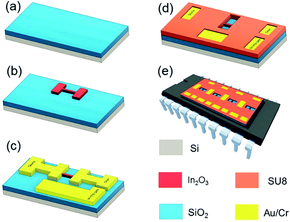 | ||
| Fig. 1 Fabrication process of In2O3 NR FETs with on-chip integrated electrode. (a and b) Pattern of In2O3 nanostructure on the SiO2/Si substrate after the first photolithography step, In2O3 deposition and lifting off; (c) define metallization feed lines, source, drain and on-chip integrated gate electrodes using Cr/Au lift-off; (d) device passivation with SU8 photoresist with open sensing area, integrated gate electrode and bonding pads; (e) packaging the In2O3 NR FET sensor into DIP 24 ceramic carrier. | ||
Device characterizations
In2O3 NRs thickness and surface roughness were measured using atomic force microscopy (AFM, Veeco Multimode 8 microscope). Wafer-scale thickness mapping of the sputtered In2O3 thin film was carried out using ellipsometry (J. A. Woollam, US). Scanning electron microscopy (SEM) imaging of the In2O3 nanoribbons was conducted with a GEMINI II SEM (Zeiss, Germany). Percentages of indium in the sputtered In2O3 thin film were measured using a Kratos X-ray photoelectron spectroscopy (XPS, Japan). Gate bias was applied from the liquid front gate via on-chip integrated Au electrodes immersed in phosphate buffer saline (1× PBS, pH 7.4, electrical conductivity 15.5 mS cm−1). In2O3 NR FETs were first washed thoroughly with acetone, propanol-2, deionized water, dried under N2 gas and treated with UV-ozone for 1 hours to remove any residual contaminants prior characterizations.After cleaning, pH measurements were carried out on un-functionalized In2O3 NR FETs. The sensors were exposed to a solution of specific pH and allowed 5 min to establish equilibrium. The transfer curves for the devices were obtained from subthreshold to max gm and over to saturation regions by scanning VGS from 0–1.5 V. The devices were washed thoroughly with deionized water and dried with a N2 stream prior to each measurement. We extracted drain current, IDS, from the transfer curves at VGS = 0.20 V (subthreshold), VGS = 0.65 V (max gm), and VGS = 1.00 V (saturation) for different pH solutions. In all pH sensing experiments and transfer characterization, VDS was fixed at 0.7 V in the saturation region of the drain voltage.
Results and discussion
Fabrication of In2O3 NR FETs, influence of nanoribbon thickness on device performance, and structural uniformity characterization
In the first part of this work, we designed and optimized a wafer-scale process for the fabrication of highly uniform In2O3 NR FET devices with excellent electrical performance. Fig. 2a shows a photographic picture of a 4-inch SiO2/Si wafer containing 22 In2O3 NR FET chips. Each chip has 4 independent NRs with corresponding on-chip integrated Au gate electrodes allowing multiplex sensing and assay control. SEM imaging of the fabricated NRs confirmed that smooth and straight In2O3 NRs (W:L: 3.7 × 14.0 μm) with source (S) and drain (D) metal electrodes were reliably fabricated throughout the whole 4-inch wafer using an optimized image reversal process (Fig. 2b). This process can be used to reliably define features down to 0.5 μm with high uniformity across the whole wafer. The RF sputtering deposition rate for In2O3 was optimized at the rate of 2.0 nm min−1, which yielded fine control over the NRs' thicknesses. As can be seen from the cross section image of a 30 nm In2O3 NR presented in Fig. 2c and d, low surface roughness (rms ∼ 1.75 nm) was obtained. Such smooth surface at the nanoscale is an important factor to achieve high FET performance as discussed in the next section.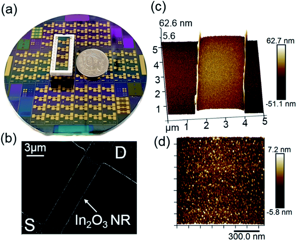 | ||
| Fig. 2 (a) Photograph of a 4-inch SiO2/Si wafer with 22 In2O3 NR FETs. On top of the wafer is a DIP packaged chip; (b) SEM image of In2O3 NR FETs with source and drain metal electrodes; (c) AFM cross-sectional image of a 30 nm In2O3 NR on Si substrate; (d) roughness characterization of the fabricated In2O3 NR (rms: 1.75 nm). | ||
In order to investigate the influence of the In2O3 FET thickness on their performance, we fabricated nanoribbons with thicknesses of 15, 60, 76, and 300 nm. The 15 nm NRs exhibited significant performance variations and low fabrication yield due to electrical contact issues to the thin film and scattering effects at such low thicknesses. For devices with thicknesses from 30 nm and upward, as the thickness of In2O3 thin film increased, subthreshold swing values increased accordingly. Specifically, subthreshold swing values increased from 80 ± 6.8 mV per decade for 30 nm devices to 88 ± 9.1 mV per decade for 60 nm devices, 121 ± 17.1 for 76 nm devices, and 140 ± 10.2 mV per decade for 300 nm devices. Representative transfer curves are shown in Fig. 3. The curves show steeper slopes in the subthreshold regime for the thinner devices. Compared to the 60, 76, and 300 nm devices, the 30 nm devices had the steepest transfer curves in the subthreshold regime and therefore the smallest SS values which can be extrapolated to the highest sensitivities. This observation is consistent with a recent report on the effect on the subthreshold swings of shrinking nanowire widths.8 It is worth to note that the SS value changes are non-linear vs. changes in sensors' thicknesses, which is typical for non-annealed amorphous metal-oxide semiconductor materials sensor. We selected 30 nm thick In2O3 films as this thickness provided the best combination between sensor performance and fabrication uniformity. Results and discussion hereafter are for 30 nm In2O3 nanoribbon devices.
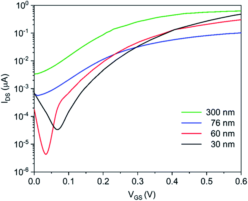 | ||
| Fig. 3 Transfer curves of In2O3 NR FETs versus thicknesses. | ||
The overarching goal of this work is to carry out a holistic investigation of the fabrication and operation of In2O3 NR FETs towards accelerating the translation of this technology into real-life applications. To this end, a quality control protocol throughout the entire fabrication process has been established to ensure high structural uniformities and material purity of the fabricated NRs. As can be seen in Fig. 4a, excellent uniformity of the patterned NRs widths is demonstrated with an average lateral dimension distribution of 3.68 ± 0.08 μm, measured from 260 NRs from 3 different batches. The wafer-scale thickness uniformity of the In2O3 NRs is also a critical factor that needs to be assessed. As shown in Fig. 4b, thickness mapping of the In2O3 sputtered on a 4-inch wafer indicated that an excellent homogeneity is achieved with a mean thickness of 28.57 nm. This translates to a degree of uniformity of 97.33%, which is better than the typical thickness uniformity of sputtered metal oxides.36
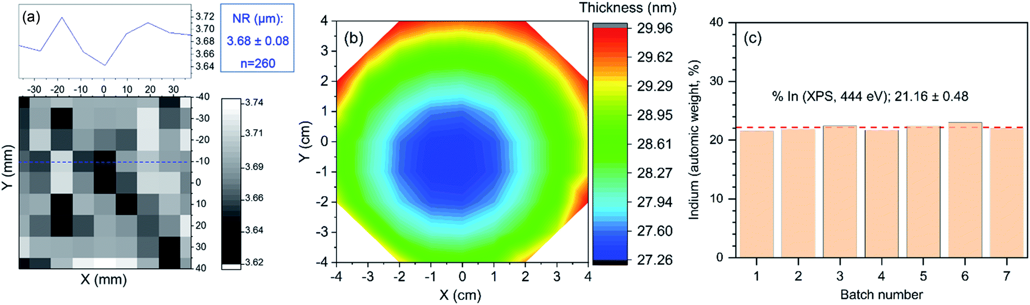 | ||
| Fig. 4 (a) Measurement profile of 260 NRs width fabricated from 3 different batches; (b) ellipsometric thickness mapping of In2O3 deposited on a 4 inch wafer; (c) XPS percentage of indium from 7 fabrication batches. | ||
Aside from sensor's structural uniformity, a consistent chemical composition of the indium oxide among fabrication batches needs to be achieved. As shown in Fig. 4c, consistent indium percentages were demonstrated with a mean indium composition of 21.1 ± 0.5%, measured from elemental indium percentage of the deposited thin films from 7 different fabrication batches. Altogether, these results confirmed that this process allows for the reproducible, cost-effective and high yield fabrication of In2O3 NR FETs and is compatible with up-scale manufacturing of this sensing technology.
Electrical characteristics of the In2O3 NR FETs
Next, the electrical performance of the fabricated In2O3 NR FETs was characterized. Fig. 5a presents the output characteristic of a device obtained by scanning the source-drain voltage, VDS, from 0.0 to 1.0 V while stepping the gate voltage, VGS, from 0 to 0.4 V (0.08 V steps) using the on-chip gate electrode. Obvious increase of the IDS in response to positive VGS within both linear and saturation regions was obtained, which is typical of a n-type enhancement long channel FET.24,25,30,37 The transfer characteristic and subthreshold parameters of the device are also presented in Fig. 5b and c, respectively. Minor kinks are also observed in the drain current presented in Fig. 5a and b. The presence of such kink effect is a typical phenomenon in direct current FET measurement, which is attributed to impact ionization and electron capture and emission at deep levels.38–41 From these graphs, the threshold voltage (Vth) of the devices were determined to be VGS = 0.35 ± 0.03 V. This low threshold voltage makes these In2O3 NR FETs devices suitable for applications requiring low power consumption such as wearable and battery powered point of care sensing. The devices' maximum transconductance gm,max was determined to be 3.93 ± 0.78 μS (n = 57). The devices' average field effect mobility was estimated to be 0.70 ± 0.14 cm2 V−1 s−1 using the following equation:23 | (1) |
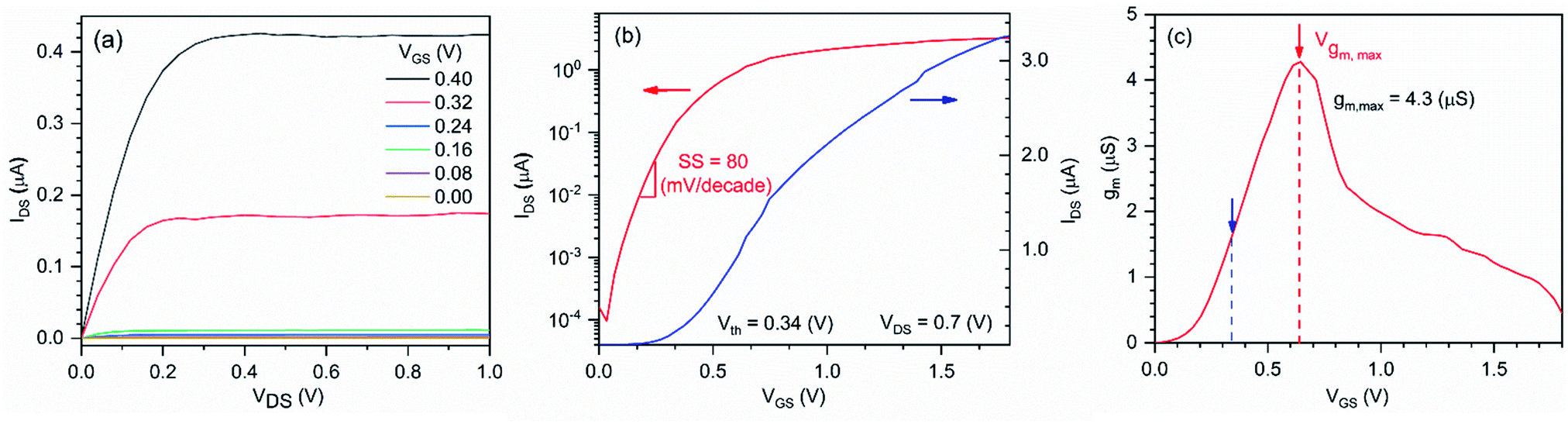 | ||
| Fig. 5 (a) Output, (b) transfer characteristics, and (c) transconductance curve of the fabricated In2O3 NR FETs. | ||
On/off current ratio was determined to be 104 to 105, which is typical for un-annealed, amorphous In2O3 NR FETs.10 Graphs presenting the statistical analyses of the 57 devices' threshold voltage, transconductance, field effect mobility and drain current on/off ratio are provided in the ESI (Fig. S3†).The leakage current was less than 5 × 10⁻¹⁰ A at VGS < 1.5 V (Fig. S1, ESI†), which is compatible with liquid measurement in bio-chemical applications.
We then investigated the subthreshold swing, a key electrical property that reflects the FET device's performance.43 As shown in Fig. 5b, the SS of the In2O3 NR FET device was determined to be 80 mV per decade, which is close to the limit of 60 mV per decade of the conventional MOSFETs44,45 and is the highest performance when compared to previously reported values for nanoribbon based In2O3 FETs (Table 1). The low SS value achieved for In2O3 NR FETs is attributed to the systematically optimized fabrication process that allows the deposition of ultra-low surface roughness indium oxide thin film with uniform composition and dimensions46,47 as well as the on-chip integration of the gate electrode.48 In particular, previous studies have shown that the surface roughness has a major impact on the performance of nanoscale transistors. This is particularly important when scaling down the thicknesses of nanoribbon FETs. Due to surface/interface trapping and phonon-scattering, smooth sensor surfaces are indeed desirable toward achieving high performance FET signals.46,47
| Fabrication route | In2O3 dimensions (W:L:H, μm) | SS (mV per decade) | Ref. |
|---|---|---|---|
| Sol–gel synthesis | 1 × 0.3 × 0.004 | 300 | 24 |
| Inkjet printing | 50 × 18 × not reported | 180 | 49 |
| Sol–gel | 70 × 3000 × 0.010 | 1800 | 50 |
| RF sputtering | 150 × 2000 × 0.008 | 250 | 51 |
| PECVD | 200 × 200 × 0.100 | 500 | 52 |
| ALD | 20 × 40 × 0.005 | 90 | 53 |
| RF sputtering | 25 × 500 × 0.016 | 300 | 9 |
| RF sputtering | 3.7 × 14 × 0.030 | 80 | This work |
Mitigating device-to-device signal variation in the subthreshold regime
It is well established that in the subthreshold regime IDS increases exponentially with VGS, while IDS only increases linearly in the linear regime. However, this intrinsic electronic differences between these two operation modes has never been exploited to reduce the device-to-device signal variations resulting from different batches. After batch-fabricating highly uniform In2O3 NR FETs, we systematically investigated the most appropriate operating bias focusing on improving the devices signal uniformity by analysing the electrical properties of 57 In2O3 NR FETs randomly selected from 3 independent different wafer-scale batches. Fig. 6a shows the plot of the mean IDS (the dots) versus applied VGS with the 95% confidence intervals (CI, the whiskers) and their respective standard deviation (SD) for each of the 57 devices. From the data, it can be seen that increasing applied VGS, measured IDS are more spread out, as shown from the larger confidence intervals and the increasing SD of IDS. However, the magnitude of device-to-device IDS variations in the subthreshold regime is comparatively lower than that measured in the linear regime. This is attributed to the intrinsic scattering of charge carriers (i.e. oxygen vacancies) within the In2O3 FET channels. When measured in a controlled environment (e.g. in a Faraday box), the variation of IDS depends on two major factors: (1) the intrinsic device electrical properties of the channel (charge carrier density, carrier mobility, variations in structural dimensions); (2) the electric field exerted on the semiconductor channel caused by the applied VGS. In our measurement, VGS was applied through large on-chip electrode (W × L: 1800 × 1400 μm, Fig. S2 in ESI†) immersed in high ionic strength electrolyte 1× PBS (∼15.5 mS cm−1) for high measurement stability. Owing to the fact that the total number of charge carriers in each thin film device is not identical as well as owing to the presence of small structural differences, increased applied VGS is expected to amplify the device-to-device differences leading in turn to larger signal variation. On the other hand, lower VGS (below Vth) only affects a portion of the charge carriers inside the In2O3 NRs, which in turn results in lower device's conductivity but also lower devices' signal variation.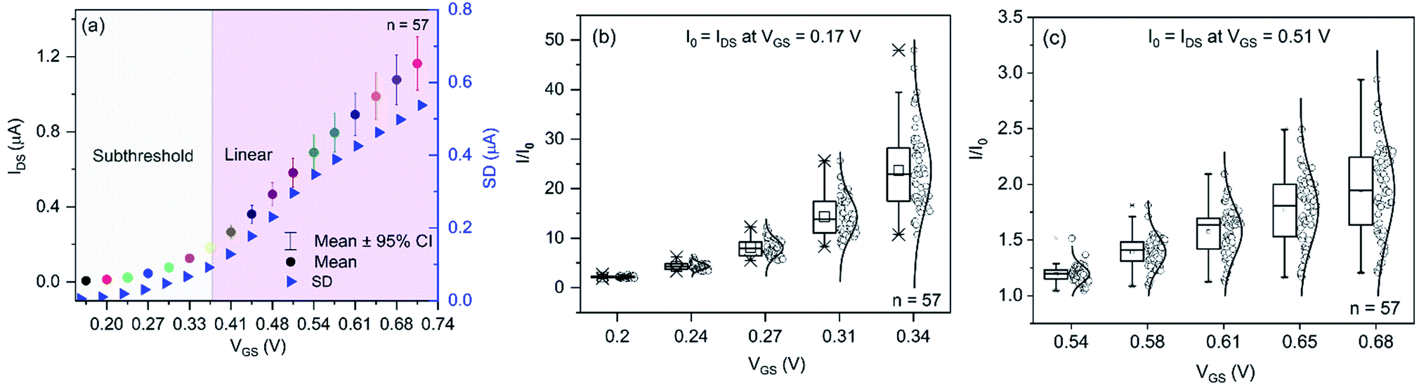 | ||
| Fig. 6 (a) Drain currents (mean values with corresponding at 95% confidence level) versus applied gate voltages in the subthreshold and linear regimes for 57 In2O3 NR FETs; (b) distributions of I/I0 of 57 In2O3 NR FETs in subthreshold (I0 = IDS at VGS = 0.17 V); and (c) in the linear regime (I0 = IDS at VGS = 0.51 V). | ||
In order to determine the optimal operational condition for reducing device-to-device signal variation, we evaluated the relative changes in I/I0 resolution when the devices are under the same magnitude of device surface potential change in the subthreshold and linear regimes. In both regimes, the normalization point, I0, was chosen as the drain current at the lowest VGS of each regime (I0 = IDS at VGS = 0.17 V for subthreshold and I0 = IDS at VGS = 0.31 V for the linear regime; detail for the IDS normalization is shown in Fig. S4 in the ESI†). When drain currents at the highest VGS of each regime are chosen as the normalization points, distributions of I/I0 values with respect to VGS in the subthreshold and linear regimes showed the same trends with more dispersed data points in the linear regime compared with the subthreshold regime (Fig. S4†). The only differences are: (1) the magnitude of I/I0 changes are now inversed to the changes when the lowest IDS are chosen as normalization points. In particular, in the subthreshold regime, on average IDS decreased 23.6 times from VGS = 0.34 V to VGS = 0.17 V when using the highest IDS as normalization point (on average IDS at VGS = 0.51 V was 0.042). On the other hand, an average increase of 23.6 times for IDS from VGS = 0.17 V to VGS = 0.34 V is obtained when using the lowest IDS as normalization point. In the linear regime, IDS increased/decreased only 2.1 times over the range of VGS = 0.68 V to VGS = 0.51 V. Because of the much bigger drain current changes over the range in the subthreshold regime, normalizing against the highest IDS compresses the data points in the lower VGS range as illustrated in the difference between Fig. 6b and S4a.† For better presentation of the data, we recommend normalizing against the lowest IDS.
Next, we proceed to determine the optimal biasing point where the NR FET devices have the highest uniformity. By characterizing electrical signals from devices of different batches, we found out that there are two combining factors that significantly suppress device-to-device signal variation in the subthreshold regime while exacerbating the issue in the linear regime (Fig. 6b and c). In the subthreshold regime, IDS increases much faster with VGS change as compared with in the linear regime. For instance, I/I0 exponentially increased an average of 22.5 times in the subthreshold regime while in the linear regime it just linearly increased by 2.1 times under the same measurement condition. At the same time, the magnitude of IDS variation in the subthreshold is lower (sub-nA to nA) than that in the linear regime (sub-μA to μA). Therefore, data distributions from the 57 devices at each VGS was better separated in the subthreshold regime as opposed to much poorer data distribution separation in the linear regime. For quantitative evaluation of data distribution separation, we calculated the quantitative resolutions (QR) of the signals using the formula:54
| QR = εr/S | (2) |
In which εr and S are the uncertainty of the measured response (variations from the 57 devices) and sensitivity (slope of calibration curve), respectively. Calibration curves for I/I0versus VGS are provided in Fig. S5, ESI.† QR is a useful figure of merit to compare device performance in different regimes as it takes into account the variability of sensitivity and the uncertainty of the measured responses.54 The smaller the QR value, the better resolved the signals. Calculated QRs for the subthreshold regime ranged from 0.009 to 0.019 V while QRs in the linear regime ranged from 0.02 to 0.08 V. The data showed that In2O3 NR FETs operated within the subthreshold regime could resolve I/I0 signal change induced by as little as VGS = 9 mV with respect to the device-to-device variation. On the other hand, at least 20 mV change in VGS is required for the FETs operated in the linear regime. Due to the exponential change in the IDS with VGS in combination with lower magnitude of device-to-device signal variation, QRs in the subthreshold regime are at least 2 times higher than those in the linear regime. For the fabricated In2O3 NR FETs, the optimal operation point was determined to be VGS = 0.15–0.2 V to achieve the best signal resolution.
Non-linear pH sensing with In2O3 NR FET
Next, the pH sensing performance of the In2O3 NR FETs was investigated from pH 10.4 to 4.0. As seen in Fig. 7, the sensors displayed more sensitive responses toward pH changes in the acidic (pH 4.0 to 7.0) compared to the basic (pH 7.0 to 10.0) pH ranges. Such non-linear pH response for the In2O3 FET can be explained by the site binding model.55 Briefly, the In2O3 NRs' surface in contact with aqueous solution can hydrogenate to form hydroxide groups (–OH groups). These groups can either protonate or deprotonate leading to changes in the surface potential of the FET. In2O3 is an inorganic amphoteric oxide with a point-of-zero charge (PZC) of approximately 9.0.56,57 This PZC results in higher pH sensitivity of the In2O3 devices in the acidic region and lower sensitivity in the more basic pH range close to the PZC because of the differences in the magnitude of surface gating caused by the changes in pH. The exponential response to pH changes in the subthreshold regime and linear response in the linear regime are attributed to the well-known exponential and linear dependences of IDS with VGS in these regimes respectively as shown experimentally in Fig. 5b and mathematically in device physics.58,59 In the saturation regime, no response to pH solution was observed as expected. An example of absolute drain current changes with pH solution is provided in Fig. 7b.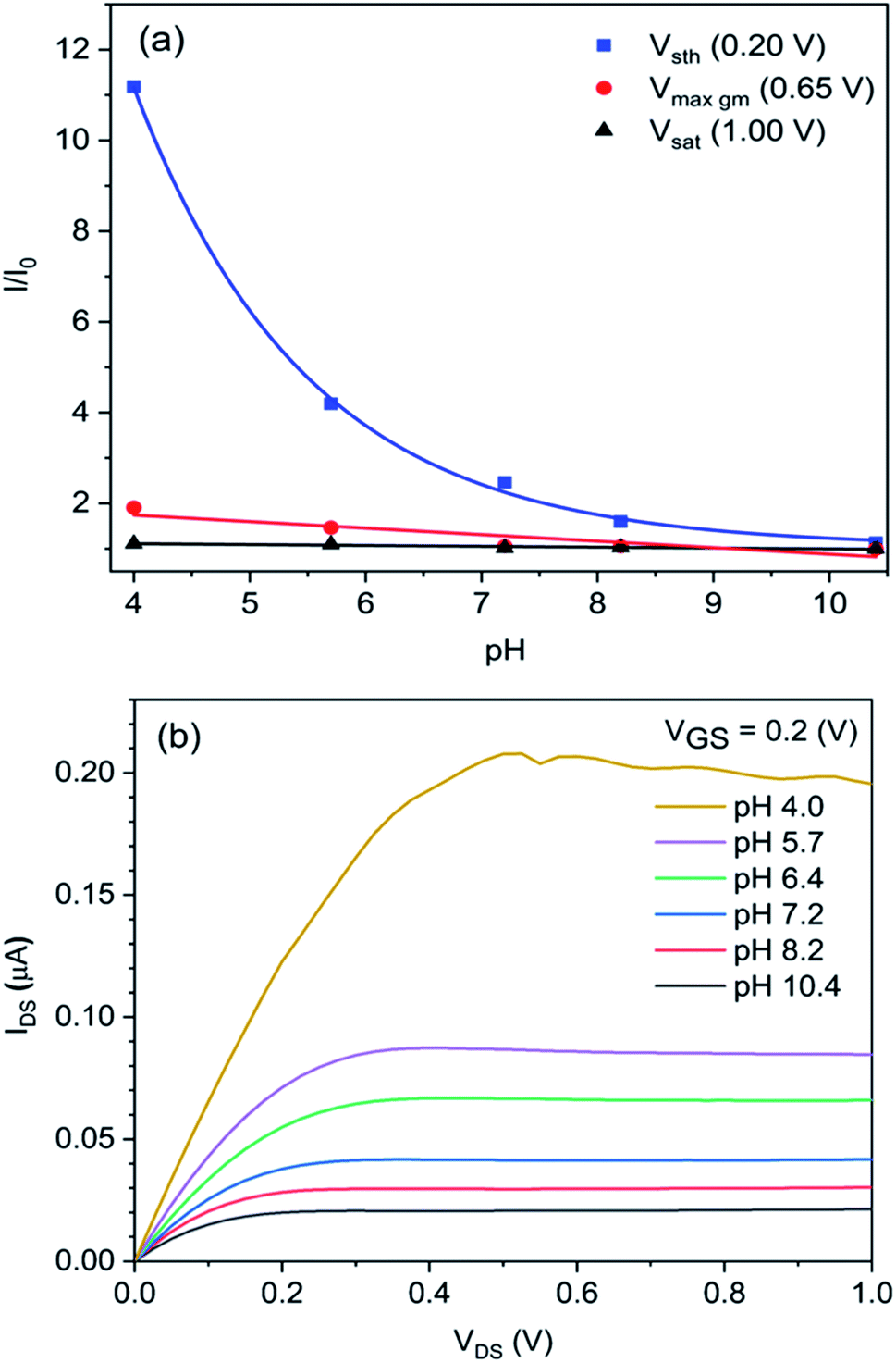 | ||
| Fig. 7 (a) pH sensing of the developed In2O3 NR FETs in different VGS regimes: subthreshold (VGS = 0.20 V), maximum transconductance (VGS = 0.65 V), and saturation (VGS = 0.10 V), VDS = 0.7 V; (b) absolute drain currents of the device with different pH values, VGS = 0.20 V. | ||
Conclusions
We report in this work a high performance In2O3 NR FET sensing platform. A steep subthreshold swing of 80 mV per decade was achieved through a combination of high quality In2O3 nanoribbon fabrication, stringent quality assessment as well as the implementation of an inbuilt gate electrode with a suitable device passivation layer. We systematically characterized and analysed the electrical properties of 57 In2O3 NR FETs from 3 different batches to reveal that device-to-device signal variation is significantly suppressed when the devices are operated in the subthreshold regime. This finding could serve as a useful operational reference for real-life sensing applications of nano FET sensors where sensing with multiple devices are required. Finally, a non-linear pH sensing response has been demonstrated on the fabricated devices. Combined with the availability of scalable and optimized fabrication processes, selecting the most appropriate operation conditions will foster the implementation of In2O3 NR FET devices in bioanalytical applications.Conflicts of interest
There are no conflicts to declare.Acknowledgements
This work is supported by the ARC Centre of Excellence in Convergent Bio-Nano Science and Technology and the DP170100170. Thuy Thi Thanh Pham acknowledges financial supports from Australia Awards Scholarships. D. P. Tran acknowledges the support of a Partnership Grant from UniSA. This work was performed in part at the South Australian and New South Wales node of the Australian National Fabrication Facility. The authors also would like to thank ANFF-SA node for their support.References
- D. Tran, T. Pham, B. Wolfrum, A. Offenhäusser and B. Thierry, Materials, 2018, 11, 785 CrossRef PubMed.
- G.-J. Zhang and Y. Ning, Anal. Chim. Acta, 2012, 749, 1–15 CrossRef CAS PubMed.
- K.-I. Chen, B.-R. Li and Y.-T. Chen, Nano Today, 2011, 6, 131–154 CrossRef CAS.
- M. O. Noor and U. J. Krull, Anal. Chim. Acta, 2014, 825, 1–25 CrossRef CAS PubMed.
- F. Patolsky, G. Zheng and C. M. Lieber, Nat. Protoc., 2006, 1, 1711–1724 CrossRef CAS PubMed.
- D. P. Tran, M. A. Winter, B. Wolfrum, R. Stockmann, C.-T. Yang, M. Pourhassan-Moghaddam, A. Offenhäusser and B. Thierry, ACS Nano, 2016, 10, 2357–2364 CrossRef CAS PubMed.
- N. Lu, A. Gao, P. Dai, S. Song, C. Fan, Y. Wang and T. Li, Small, 2014, 10, 2022–2028 CrossRef CAS PubMed.
- K. Shoorideh and C. O. Chui, Proc. Natl. Acad. Sci. U. S. A., 2014, 111, 5111–5116 CrossRef CAS PubMed.
- Q. Liu, N. Aroonyadet, Y. Song, X. Wang, X. Cao, Y. Liu, S. Cong, F. Wu, M. E. Thompson and C. Zhou, ACS Nano, 2016, 10, 10117–10125 CrossRef CAS PubMed.
- N. Aroonyadet, X. Wang, Y. Song, H. Chen, R. J. Cote, M. E. Thompson, R. H. Datar and C. Zhou, Nano Lett., 2015, 15, 1943–1951 CrossRef CAS PubMed.
- H.-K. Chang, F. N. Ishikawa, R. Zhang, R. Datar, R. J. Cote, M. E. Thompson and C. Zhou, ACS Nano, 2011, 5, 9883–9891 CrossRef CAS PubMed.
- M. Curreli, C. Li, Y. Sun, B. Lei, M. A. Gundersen, M. E. Thompson and C. Zhou, J. Am. Chem. Soc., 2005, 127, 6922–6923 CrossRef CAS PubMed.
- A. L. D. Moreau, R. Janissen, C. A. Santos, L. A. Peroni, D. R. Stach-Machado, A. A. de Souza, A. P. de Souza and M. A. Cotta, Biosens. Bioelectron., 2012, 36, 62–68 CrossRef CAS PubMed.
- S. Upadhyay, R. Frederiksen, N. Lloret, L. D. Vico, P. Krogstrup, J. H. Jensen, K. L. Martinez and J. Nygård, Appl. Phys. Lett., 2014, 104, 203504 CrossRef.
- R. Janissen, P. K. Sahoo, C. A. Santos, A. M. da Silva, A. A. G. von Zuben, D. E. P. Souto, A. D. T. Costa, P. Celedon, N. I. T. Zanchin, D. B. Almeida, D. S. Oliveira, L. T. Kubota, C. L. Cesar, A. P. d. Souza and M. A. Cotta, Nano Lett., 2017, 17, 5938–5949 CrossRef CAS PubMed.
- C. Li, M. Curreli, H. Lin, B. Lei, F. N. Ishikawa, R. Datar, R. J. Cote, M. E. Thompson and C. Zhou, J. Am. Chem. Soc., 2005, 127, 12484–12485 CrossRef CAS PubMed.
- S. Liu and X. Guo, NPG Asia Mater., 2012, 4, e23 CrossRef.
- M. L. Hammock, O. Knopfmacher, T. N. Ng, J. B. Tok and Z. Bao, Adv. Mater., 2014, 26, 6138–6144 CrossRef CAS PubMed.
- V. Krivitsky, L.-C. Hsiung, A. Lichtenstein, B. Brudnik, R. Kantaev, R. Elnathan, A. Pevzner, A. Khatchtourints and F. Patolsky, Nano Lett., 2012, 12, 4748–4756 CrossRef CAS PubMed.
- O. Knopfmacher, A. Tarasov, W. Fu, M. Wipf, B. Niesen, M. Calame and C. Schönenberger, Nano Lett., 2010, 10, 2268–2274 CrossRef CAS PubMed.
- G. S. Kulkarni and Z. Zhong, Nano Lett., 2012, 12, 719–723 CrossRef CAS PubMed.
- P. E. Sheehan and L. J. Whitman, Nano Lett., 2005, 5, 803–807 CrossRef CAS PubMed.
- Q. Liu, Y. Liu, F. Wu, X. Cao, Z. Li, M. Alharbi, A. N. Abbas, M. R. Amer and C. Zhou, ACS Nano, 2018, 12, 1170–1178 CrossRef CAS PubMed.
- J. Kim, Y. S. Rim, H. Chen, H. H. Cao, N. Nakatsuka, H. L. Hinton, C. Zhao, A. M. Andrews, Y. Yang and P. S. Weiss, ACS Nano, 2015, 9, 4572–4582 CrossRef CAS PubMed.
- C. Li, B. Lei, D. Zhang, X. Liu, S. Han, T. Tang, M. Rouhanizadeh, T. Hsiai and C. Zhou, Appl. Phys. Lett., 2003, 83, 4014–4016 CrossRef CAS.
- X. Zou, X. Liu, C. Wang, Y. Jiang, Y. Wang, X. Xiao, J. C. Ho, J. Li, C. Jiang, Q. Xiong and L. Liao, ACS Nano, 2013, 7, 804–810 CrossRef CAS PubMed.
- D. Zhang, Z. Liu, C. Li, T. Tang, X. Liu, S. Han, B. Lei and C. Zhou, Nano Lett., 2004, 4, 1919–1924 CrossRef CAS.
- W. J. Maeng, D.-w. Choi, K.-B. Chung, W. Koh, G.-Y. Kim, S.-Y. Choi and J.-S. Park, ACS Appl. Mater. Interfaces, 2014, 6, 17481–17488 CrossRef CAS PubMed.
- J. Sheng, D.-w. Choi, S.-H. Lee, J. Park and J.-S. Park, J. Mater. Chem. C, 2016, 4, 7571–7576 RSC.
- J. H. Noh, S. Y. Ryu, S. J. Jo, C. S. Kim, S. W. Sohn, P. D. Rack, D. J. Kim and H. K. Baik, IEEE Electron Device Lett., 2010, 31, 567–569 CAS.
- Z. Yuan, X. Zhu, X. Wang, X. Cai, B. Zhang, D. Qiu and H. Wu, Thin Solid Films, 2011, 519, 3254–3258 CrossRef CAS.
- S. K. Garlapati, T. T. Baby, S. Dehm, M. Hammad, V. S. K. Chakravadhanula, R. Kruk, H. Hahn and S. Dasgupta, Small, 2015, 11, 3591–3596 CrossRef CAS PubMed.
- F. N. Ishikawa, M. Curreli, H.-K. Chang, P.-C. Chen, R. Zhang, R. J. Cote, M. E. Thompson and C. Zhou, ACS Nano, 2009, 3, 3969–3976 CrossRef CAS PubMed.
- M. O. Hill, I. Calvo-Almazan, M. Allain, M. V. Holt, A. Ulvestad, J. Treu, G. Koblmüller, C. Huang, X. Huang, H. Yan, E. Nazaretski, Y. S. Chu, G. B. Stephenson, V. Chamard, L. J. Lauhon and S. O. Hruszkewycz, Nano Lett., 2018, 18, 811–819 CrossRef CAS PubMed.
- S. Labat, M.-I. Richard, M. Dupraz, M. Gailhanou, G. Beutier, M. Verdier, F. Mastropietro, T. W. Cornelius, T. U. Schülli, J. Eymery and O. Thomas, ACS Nano, 2015, 9, 9210–9216 CrossRef CAS PubMed.
- M. Matsuoka and S. i. Tohno, J. Vac. Sci. Technol., A, 1995, 13, 2427–2434 CrossRef CAS.
- C.-H. Choi, S.-Y. Han, Y.-W. Su, Z. Fang, L.-Y. Lin, C.-C. Cheng and C.-h. Chang, J. Mater. Chem. C, 2015, 3, 854–860 RSC.
- J. Haruyama, H. Negishi, Y. Nishimura and Y. Nashimoto, IEEE Trans. Electron Devices, 1997, 44, 25–33 CrossRef CAS.
- J. Haruyama, Y. Ohno, H. Katano and Y. Nashimoto, IEEE Trans. Electron Devices, 1994, 41, 1873–1875 CrossRef CAS.
- K. Kato, T. Wada and K. Taniguchi, IEEE Trans. Electron Devices, 1985, 32, 458–462 Search PubMed.
- M. Narayanan, H. Al-Nashash, B. Mazhari, D. Pal and M. Chandra, Act. Passive Electron. Compon., 2012, 2012, 1–9 CrossRef.
- S. Park, S. Lee, C.-H. Kim, I. Lee, W.-J. Lee, S. Kim, B.-G. Lee, J.-H. Jang and M.-H. Yoon, Sci. Rep., 2015, 5, 13088 CrossRef CAS PubMed.
- W. Cao, D. Sarkar, Y. Khatami, J. Kang and K. Banerjee, AIP Adv., 2014, 4, 067141 CrossRef.
- Q. Xu, X. Liu, B. Wan, Z. Yang, F. Li, J. Lu, G. Hu, C. Pan and Z. L. Wang, ACS Nano, 2018, 12, 9608–9616 CrossRef CAS PubMed.
- Z. Qin, Z. Wei and A. Seabaugh, IEEE Electron Device Lett., 2006, 27, 297–300 Search PubMed.
- F. Wang, S. Yip, N. Han, K. Fok, H. Lin, J. J. Hou, G. Dong, T. Hung, K. S. Chan and J. C. Ho, Nanotechnology, 2013, 24, 375202 CrossRef PubMed.
- D. P. Tran, B. Wolfrum, R. Stockmann, A. Offenhäusser and B. Thierry, J. Mater. Chem. C, 2014, 2, 5229–5234 RSC.
- H. J. N. P. D. Mello, S. Dalgleish, G. Ligorio, M. Mulato and E. J. W. List-Kratochvil, Organic and Hybrid Sensors and Bioelectronics XI, SPIE Proceedings, 2018, vol. 10738, p. 1073819 Search PubMed.
- H. Basem, L. You, Y. Jason, Y. Yang, G. Kumaravelu, W. Andrew, E. Robin, C. Gursharan, N. Babak and S. Efstratios, Flexible Printed Electron., 2018, 3, 042001 CrossRef.
- C. Kookhyun, K. Minseok, C. Seongpil, O. Tae-Yeon, J. Shin Woo, H. Hyeon Jun and J. Byeong-Kwon, Jpn. J. Appl. Phys., 2013, 52, 060204 CrossRef.
- J. H. Noh, S. Y. Ryu, S. J. Jo, C. S. Kim, S. Sohn, P. D. Rack, D. Kim and H. K. Baik, IEEE Electron Device Lett., 2010, 31, 567–569 CAS.
- Y. Vygranenko, K. Wang and A. Nathan, Appl. Phys. Lett., 2007, 91, 263508 CrossRef.
- H. I. Yeom, J. B. Ko, G. Mun and S. H. K. Park, J. Mater. Chem. C, 2016, 4, 6873–6880 RSC.
- H. L. Pardue, Clin. Chem., 1997, 43, 1831 CAS.
- D. E. Yates, S. Levine and T. W. Healy, J. Chem. Soc., Faraday Trans. 1, 1974, 70, 1807–1818 RSC.
- J. A. R. M. Fernández-García, Synthesis, Properties, and Applications of Oxide Nanomaterials, John Wiley & Sons, Inc., Hoboken, NJ, USA, 2006, ch. 2, pp. 49–78, ISBN: 978-0-471-72405-6 Search PubMed.
- M. Kosmulski, J. Colloid Interface Sci., 2001, 238, 225–227 CrossRef CAS PubMed.
- W. Deng, X. Ma and J. Huang, AIP Adv., 2014, 4, 087107 CrossRef.
- W. Deng and J. Huang, IEEE Electron Device Lett., 2011, 32, 647–649 CAS.
Footnote |
| † Electronic supplementary information (ESI) available. See DOI: 10.1039/c9na00592g |
| This journal is © The Royal Society of Chemistry 2019 |