
 Open Access Article
 This Open Access Article is licensed under a Creative Commons Attribution-Non Commercial 3.0 Unported Licence
Laser induced ion migration in all-inorganic mixed halide perovskite micro-platelets†
Ziming
Wang
a,
Yue
Wang
 *a,
Zhonghui
Nie
a,
Yinjuan
Ren
b and
Haibo
Zeng
*a
*a,
Zhonghui
Nie
a,
Yinjuan
Ren
b and
Haibo
Zeng
*a
aMIIT Key Laboratory of Advanced Display Materials and Devices, Institute of Optoelectronics & Nanomaterials, College of Materials Science and Engineering, Nanjing University of Science and Technology, Nanjing 210094, China. E-mail: ywang@njust.edu.cn; zeng.haibo@njust.edu.cn
bDepartment of Chemistry, National University of Singapore, 3 Science Drive 3, Singapore 117543, Singapore
First published on 8th October 2019
Abstract
Despite intensive research on ion migration (IM) in organic–inorganic hybrid metal halide perovskites, much less is known about the irradiation effect on IM in all-inorganic perovskites, especially for those single crystals lacking complicated grain boundaries. Herein, the real-time IM process and the corresponding photoluminescence (PL) spectra induced by laser irradiation in all-inorganic CsPbBrxI(3−x) single crystals prepared by chemical vapor deposition (CVD) were investigated. We proposed that a local electric field acts as a driving force for IM and confirmed this by applying a bias to an indium tin oxide (ITO)/perovskite/ITO configuration. According to the control experiments on CsPbBrxI(3−x) micro-platelets with and without polymethyl methacrylate (PMMA) coating, it is concluded that the vacancy defect on the single crystal surface is the main pathway for IM. Our work is important for understanding and controlling light induced IM in all-inorganic perovskites.
Introduction
Metal halide perovskites composed of ABX3 (A = methylammonium ion (MA+), formamidine ion (FA+) or Cs+; B = Pb2+; X = Cl−, Br− or I− or a mixture thereof) are attractive in the fields of light-emitting diodes (LEDs),1 lasers,2,3 photodetectors4,5 and solar cells6–11 thanks to their adjustable band gap,12 long carrier diffusion length13,14 and large tolerance to defects.15 As the most distinguished feature in ionic crystals, ion migration (IM) was found to be correlated with many unusual phenomena observed in halide perovskites. For example, Hoke and co-workers reported that under light illumination, the photoluminescence (PL) spectrum of mixed halide perovskites would have a gradual red-shift, accompanied by the corresponding X-ray diffraction peak splitting, which means that two independent phases were formed.16 Different from Hoke's work, Zhang and co-workers found that an abnormal blue shift in the PL spectrum took place due to iodide migration and evaporation under laser irradiation in mixed halide perovskites.17 Moreover, by combining experimental and theoretical calculations, Meloni and co-workers have proved that the halide IM induced polarization of the perovskite layer causes current hysteresis in solar cells.18To understand IM in halide perovskites, a number of studies have been done on organic–inorganic hybrid metal halide perovskites (MAPbBrxI(3−x)), especially polycrystalline films. It has been reported that large density of point defects, lattice distortion and grain boundaries are the main migration paths in perovskite films.9,16,17,19–21 The basic path is dominated by defects in the materials.22 On the other hand, understanding the driving force for IM in halide perovskites is also an important issue. According to previous studies, localized strain generated by a single photoexcited charge interacting with the soft ionic lattice23 or the piezoelectric effect24 will promote IM. Nevertheless, organic–inorganic hybrid perovskites are notoriously unstable,25,26 such that focused probing laser beams or a high energy detection method will damage the crystal structure of the perovskites, making the phase separation process more complicated.
All-inorganic perovskites are known to exhibit improved stability and many different properties have been demonstrated in inorganic perovskites compared to hybrid perovskites. Until now, investigations on IM in all-inorganic perovskites are still rare. Furthermore, most of the IM studies were done on polycrystalline films or nanocrystals, where the rich grain boundaries and large surface-to-volume ratio are considered to complicate the IM phenomenon. Single crystals of inorganic perovskites have been fabricated by the chemical vapor deposition (CVD) method, and have demonstrated much improved optoelectronic performance.27 The natural question is how IM behaves in inorganic perovskite single crystals, which could reflect the intrinsic properties of IM in the material and, thus, are important for both fundamental research and technological applications.
In this work, we observed the real-time IM process under laser irradiation in the all-inorganic hybrid halide CsPbBrxI(3−x) micro-platelet single crystal prepared by the CVD method. With the increase of laser irradiation time, the PL peak splits from a single emission peak into two emission peaks, corresponding to the emission peaks of the iodine-rich domain and the bromine-rich domain, respectively. We demonstrated that the local electric field generated by the photocarrier trapping acts as a driving force for IM by applying a bias to an indium tin oxide (ITO)/perovskite/ITO configuration. According to the experimental observations, the detailed IM process was proposed. By coating a thin PMMA layer on the surface of the sample, we proved that the vacancy on the surface of the perovskite single crystal is the main channel for IM and, hence, put forward a strategy to control the IM by surface engineering. Finally, the laser induced IM was exploited to make photo-patterns in the perovskite microcrystals in a programmable manner, which may find applications in information encoding and anti-counterfeiting.
Results and discussion
The CsPbBrxI(3−x) micro-platelets were grown by the CVD method (see detailed fabrication procedures in the Experimental section). Similar to previous reports,28 the micro-platelets exhibit a regular cubic shape, manifesting the single crystalline nature. The lateral sizes of the microplates are of several tens of micrometers and thickness of hundreds of nanometers determined by the atomic force microscopy (AFM) measurements (Fig. S2†). According to the AFM measurements, the average roughness is determined to be ∼3.77 nm. Fig. 1a shows the steady-state PL spectrum of a CsPbBrxI(3−x) micro-platelet. A single emission peak appears at 566 nm, which red-shifts about 41 nm compared with CsPbBr3 perovskites. This indicates the formation of mixed halide perovskite CsPbBrxI(3−x).Fig. 1b presents the scanning electron microscopy (SEM) image of CsPbBrxI(3−x) micro-platelets and the corresponding elemental mapping from energy dispersive X-ray spectroscopy (EDX) measurements is displayed in Fig. S1,† which shows that the Cs, Pb, Br and I elements are uniformly distributed.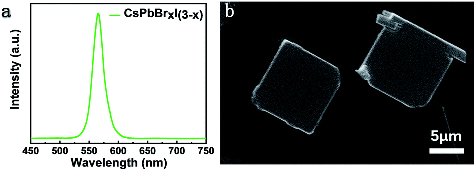 | ||
| Fig. 1 (a) Steady-state PL spectrum of a CsPbBrxI(3−x) micro-platelet. (b) SEM of two CsPbBrxI(3−x) micro-platelets; the scale bar is 5 μm. | ||
As presented in Fig. 2b, the steady-state PL spectra of the cubic shape individual CsPbBrxI(3−x) micro-platelet have been measured under laser irradiation. The PL of untreated micro-platelet peaks at 566 nm. Continuous laser irradiation (405 nm, excitation intensity: Iexc = 20 W cm−2) over 60 seconds caused the appearance of the emission peak at 680 nm, which represents the formation of a typical iodine-rich phase and confirms the occurrence of phase segregation as the peak position blue-shifts about 20 nm compared to that of CsPbI3. Interestingly, our observation is different from phase segregation discovered previously, where studies showed a continuous redshift of the PL peak under the continuous illumination.16,19,29 Here, we got two separated emission peaks, corresponding to bromine-rich phase emission with the PL wavelength between 525 nm and 600 nm and iodine-rich phase emission with the PL wavelength between 625 nm and 725 nm. With the increase of laser irradiation time (0–12 min), PL from the bromine-rich phase decreases while iodine-rich phase PL exhibits a monotonous increase and then stabilizes at a higher intensity (Fig. 2b). Moreover, this IM phenomenon is reversible, as shown in Fig. 2c. When turning off the laser, iodine-rich phase PL intensity decreases while bromine-rich phase PL intensity gradually recovers to 24% of the initial value after 35 minutes. In order to show the increasing trend of the iodine-rich phase under laser irradiation more clearly, we normalized the PL spectra based on the luminescence peak of the bromine-rich phase (Fig. S3a†). Meanwhile, to demonstrate the recovery process of the bromine-rich phase PL intensity in the dark environment more clearly, we normalized it based on the luminescence peak of the iodine-rich phase (Fig. S3b†).
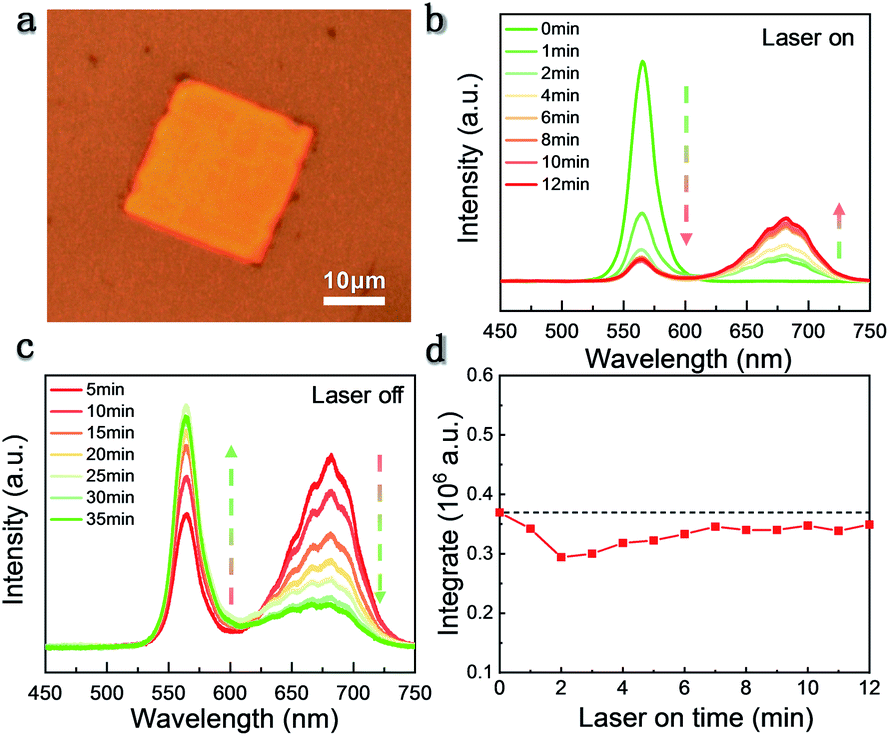 | ||
| Fig. 2 (a) Optical picture of an individual CsPbBrxI(3−x) micro-platelet, and the scale bar is 10 μm. (b) The PL spectral change of an individual CsPbBrxI(3−x) micro-platelet under continuous laser irradiation. (c) The PL spectra measured for the same position after the laser irradiation had been turned off. At each time point, the laser was turned on for 10 s to acquire the PL spectra. (d) The integrated intensity of the PL spectrum in the wavelength of 500 nm to 750 nm. | ||
The integrated intensity of the PL spectrum in a wavelength of 500 nm to 750 nm is shown in Fig. 2d. With the increase of laser irradiation time, the integrated intensity decreases slightly at the beginning. Two minutes later, the intensity slowly recovers and stabilizes near the initial value. This phenomenon indicates that the phase segregation due to laser irradiation does not damage the sample or increase the defect density in the sample. We have also repeated similar experiments on other samples with different halide ratios by changing the molar ratio of PbBr2 and CsI precursors (see Fig. S4 and S5†), and a similar laser-induced PL phenomenon was observed, indicating that this IM phenomenon is general in mixed-halide perovskites.
Fig. 3a shows the micrograph of CsPbBrxI(3−x) micro-platelets in bright field. The laser-irradiated fluorescence micrographs were taken at 0 s, 20 s, 60 s, 90 s, 120 s, 150 s, 180 s, 210 s, 240 s, 270 s and 300 s in dark field in Fig. 3b-l. With the extension of irradiation time, the CsPbBrxI(3−x) micro-platelet emits strong green light at 0 s and is gradually dominated by red luminescence at 300 s. The whole change process is consistent with the PL test results in Fig. 2b, which further confirms the presence of light induced IM.
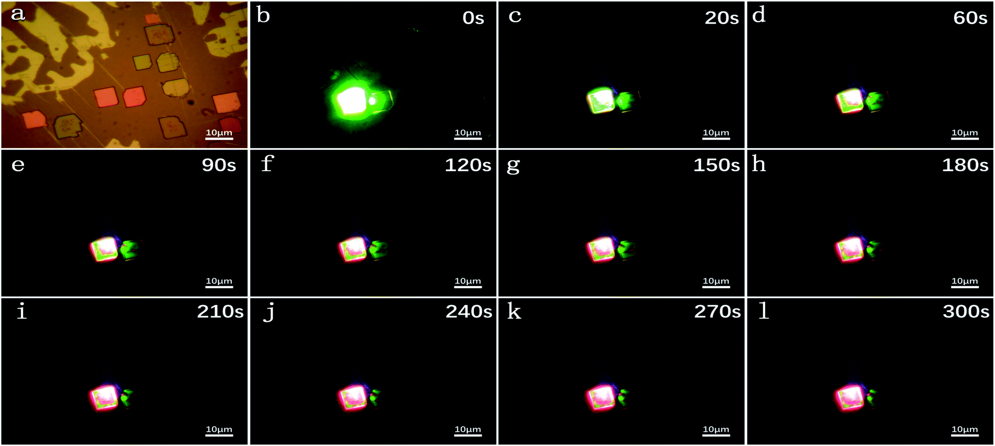 | ||
| Fig. 3 (a) Optical picture of CsPbBrxI(3−x) micro-platelets in bright field. (b-l) Laser-irradiated fluorescence micrographs taken at 0 s, 20 s, 60 s, 90 s, 120 s, 150 s, 180 s, 210 s, 240 s, 270 s and 300 s in dark field. The scale bar is 10 μm. | ||
In previous reports, a similar light induced IM phenomenon has also been observed in organic–inorganic halide perovskite polycrystalline films and nanocrystals. It is suggested that the defects on the grain boundaries could capture the photo-excited carriers which can give rise to a local electric field. The electrical field arising from spatial charge separation30 will lead to IM. Recently, a local compressive strain due to the piezoelectric effect was reported to promote IM as well.24 To verify the influence of the electric field on the phase segregation effect in our sample, we fabricated CsPbBrxI(3−x) single crystal micro-platelets to form an ITO/perovskite/ITO configuration as shown in Fig. 4a. First, we measured the PL spectra of an individual CsPbBrxI(3−x) micro-platelet under continuous laser irradiation without electrical biasing (Fig. 4b). It is found that the bromine-rich phase emission intensity declines while the iodine-rich phase emission intensity increases during laser irradiation, indicating that IM has occurred. Then, we applied an external electrical bias between the two ITO electrodes and turned off the laser. We only turned on the laser for a few seconds when we recorded the PL spectra. It can be seen that the emission intensity of the bromine-rich phase still decreases while iodine-rich phase intensity keeps increasing (Fig. 4c). As a result, it can be concluded that the applied electric field has a similar promotion effect on IM in CsPbBrxI(3−x) micro-platelets. These findings indicate that the local electric field generated by the photocarrier trapping acts as a driving force for IM in inorganic mixed halide perovskites.
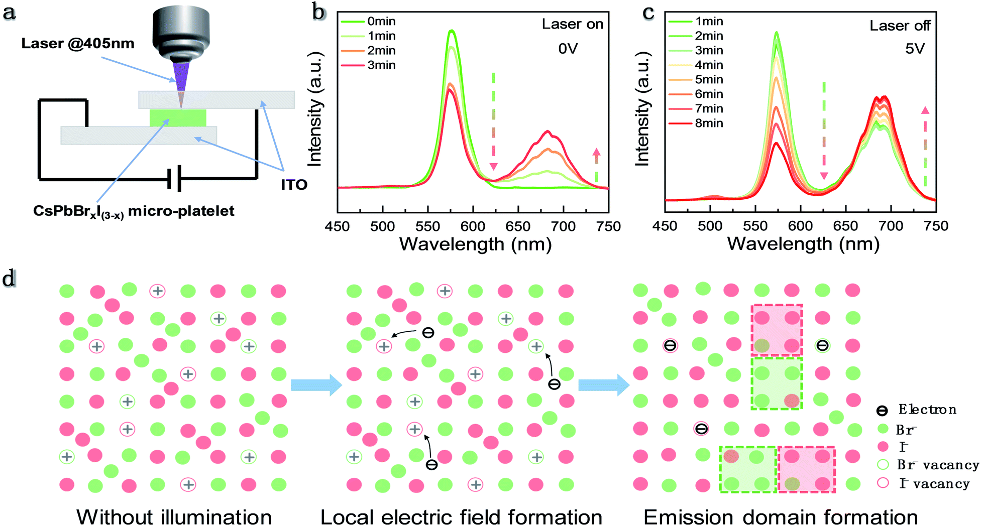 | ||
| Fig. 4 (a) Schematic diagram of the applied electric field measurement. (b) The PL spectral change of an individual CsPbBrxI(3−x) micro-platelet under continuous laser irradiation without electrical biasing. (c) The PL spectra measured for the same position with an electrical bias in the dark. At each time point, the laser was turned on for 10 s to acquire the PL spectra. (d) Schematic diagram of the IM process and the emission domain formation process. (The minus sign represents the electron. The red solid circles, the green solid circles, the red hollow circles and the green hollow circles refer to iodine ions, bromine ions, iodine vacancies and bromine vacancies, respectively). | ||
According to the observations, the mechanism for the IM behavior in CsPbBrxI(3−x) micro-platelets can be proposed and schematically shown in Fig. 4d. During the CsPbBrxI(3−x) micro-platelet formation and cooling process, defects would be inevitably generated in the samples.27 Upon laser excitation, the photocarriers will be trapped by the defects and create a local electrical field. Coulombic repulsion between halide ions and the local electric field prompts the migration of halide ions. During the migration process, the basic unit is formed which consists of the bromine-rich phase and iodine-rich phase. In each unit, photogenerated free carriers funnel and recombine in the new lowest-energy states within the iodide-rich phase22 causing the emission with the PL wavelength between 625 nm and 725 nm. It is reported that the polarons formed by carrier–lattice interaction can stabilize the bromine-rich and iodine-rich units due to the much larger mobility of the excess charge relative to the halide ions.23 These stabilized units continue to accumulate, resulting in an increase (decrease) of iodine-rich (bromine-rich) phase PL intensity and the nearly constant PL peak positions.
It is known that high point defect density or lattice distortion could provide multiple channels for IM.7,9,16,19,20 As for polycrystalline films, grain boundaries possess rich defects and are recognized as the chief culprit for IM.17–21 In view of the perovskite single crystals which are free of grain boundaries, the dominant carrier-trapping centers are unravelled to be the surface defects.31 According to previous theoretical studies, halide vacancies have the lowest activation energy (Ea) where the Ea is calculated to be 0.8–2.31, 0.59–1.20, 0.09–0.27 and 0.08–0.58 eV for the Pb2+, Cs+, Br− and I− vacancies,7,32 respectively. Therefore, it is expected that the halide vacancies on the surface of the micro-platelets are the main migration path rather than the metal vacancies. To verify the hypothesis, we applied a thin PMMA layer on the surface of the sample which has been widely used for surface passivation in many traditional semiconductors.33 The micrograph of CsPbBrxI(3−x) micro-platelets covered with a layer of PMMA is shown in Fig. 5a. The PL and the PL decay of the CsPbBrxI(3−x) micro-platelet with and without PMMA were tested by the steady-state and time-resolved PL measurements. The PL intensity was found to increase by about 3 times when the micro-platelet was covered with a layer of PMMA (Fig. 5c). Simultaneously, the slow component34 in the PL decay was suppressed in the corresponding time-resolved fluorescence. These results indicated that applying a layer of PMMA to the surface of the CsPbBrxI(3−x) micro-platelet could reduce the surface vacancies, supporting the passivation effect. Afterwards, we performed the same experiment by monitoring the PL of the PMMA-covered sample under laser irradiation (Fig. 5b). It is found that the magnitude of the PL variation from the sample coated with PMMA is much smaller than those without PMMA passivation. Furthermore, we quantitatively analyzed the magnitude of the relative PL change of the samples with and without PMMA during continuous laser irradiation (Fig. S6a and b†). After laser irradiation for 12 min, for the sample without PMMA, the PL intensity of the iodine-rich phase has been increased to be 2.38 times that of the bromine-rich phase, while for the sample covered with PMMA, the iodine-rich phase PL intensity is only 45% of that of the bromine-rich phase under the same experimental conditions. These results confirm the conjecture that vacancies on the surface serve as the main ion transport path. Besides, the finding provides an enabling strategy to suppress the IM in perovskite crystals by suitable surface treatment. Fig. 5e illustrates the migration path of surface vacancies and the suppression of IM by surface passivation (Fig. 5f). Coating a layer of PMMA on the surface of the sample is a facile method for surface passivation. Similarly, other surface passivation methods, such as the atomic layer deposition (ALD), should also be feasible to heal the surface defects and control the IM in halide perovskite crystals.
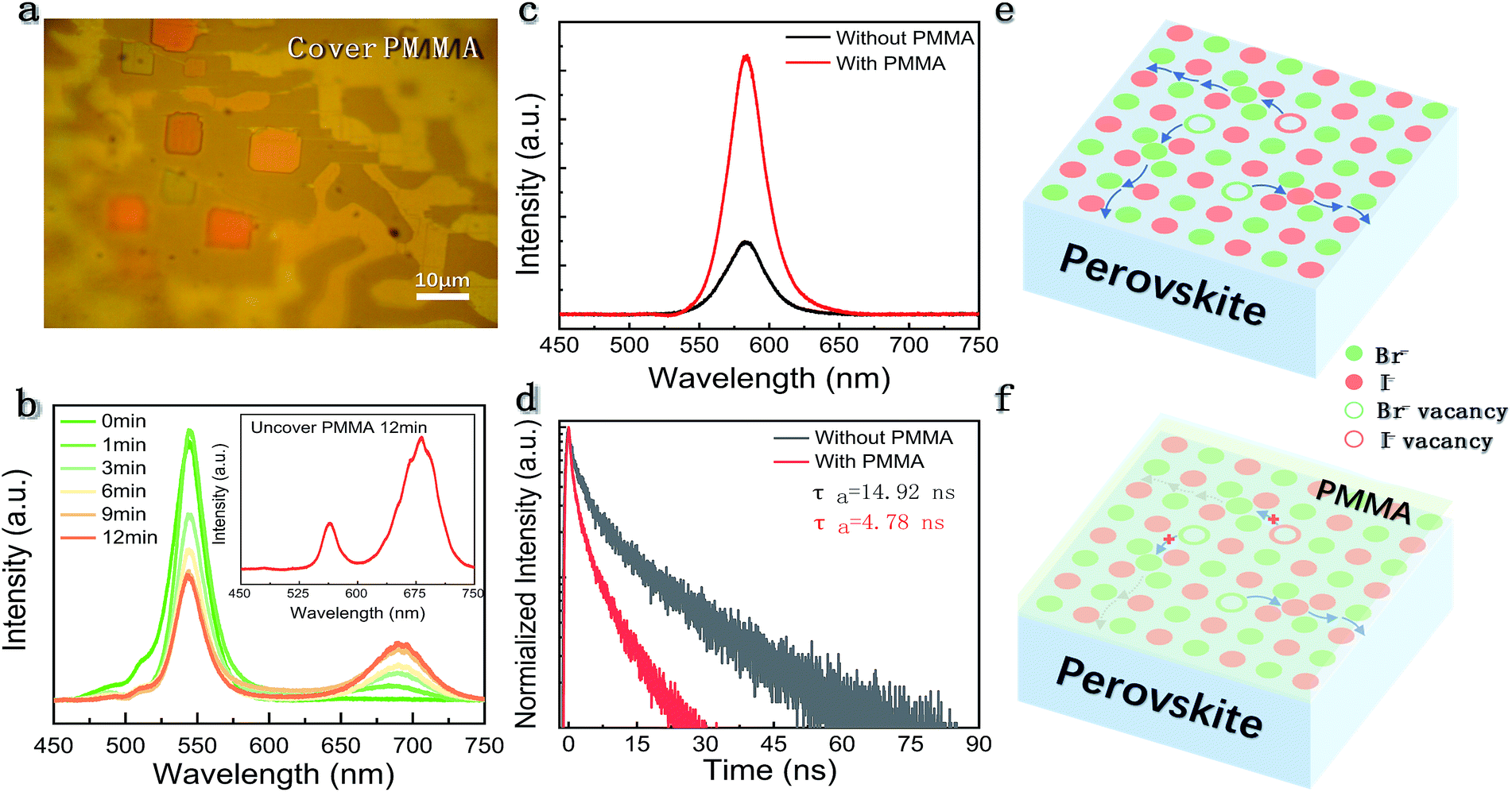 | ||
| Fig. 5 (a) Optical picture of CsPbBrxI(3−x) micro-platelets covered with a layer of PMMA, and the scale bar is 10 μm. (b) The PL spectral change of an individual CsPbBrxI(3−x) micro-platelet covered with a layer of PMMA during continuous laser irradiation. The inset shows the PL spectra of CsPbBrxI(3−x) micro-platelets without PMMA after laser irradiation for 12 min. (c) PL spectra of the initial individual CsPbBrxI(3−x) micro-platelet with (red line) and without (black line) PMMA, respectively. (d) Time-resolved fluorescence profiles of the individual CsPbBrxI(3−x) micro-platelet with (red line) and without (black line) PMMA, respectively. (e) Movement path of perovskite surface vacancies. (f) Illustration of the passivation of CsPbBrxI(3−x) micro-platelet surface vacancies by PMMA. (The red solid circles, the green solid circles, the red hollow circles and the green hollow circles refer to iodine ions, bromine ions, iodine vacancies and bromine vacancies, respectively). | ||
The IM may not always be detrimental and interesting applications can be enabled given that IM is properly controlled. Here, we show that photo-induced IM can be exploited to make heterostructures or photo-patterns in the perovskite microcrystals in a programmable manner. Fig. 6a shows the schematic diagram of the experimental configuration for the photopattern fabrication. The position of the sample can be controlled by a three-dimensional translation stage. At the beginning of laser irradiation, the CsPbBrxI(3−x) micro-platelet emits pure green fluorescence similar to that in Fig. 3. We adjusted the three-dimensional translation stage along the square path to control the movement of the sample. Ten seconds later, the color of fluorescence began to change (Fig. 6b). After 300 seconds of operation, the area illuminated by the laser emits red light, and with a square outline, the area that is not illuminated remains green (Fig. 6c). The minimum limit radius of the laser spot in our experiment is ∼2 microns, which is still very large for accurate pattern preparation. If the laser spot is small enough, the precise design and preparation of the pattern can be realized. By adjusting the laser irradiation time and laser intensity, the relative proportions of the two colors can also be adjusted accordingly. The proof-of-concept experiment indeed demonstrates that the photo-induced IM can be used to make photo-patterns, which may find applications in information encoding and anticounterfeiting.
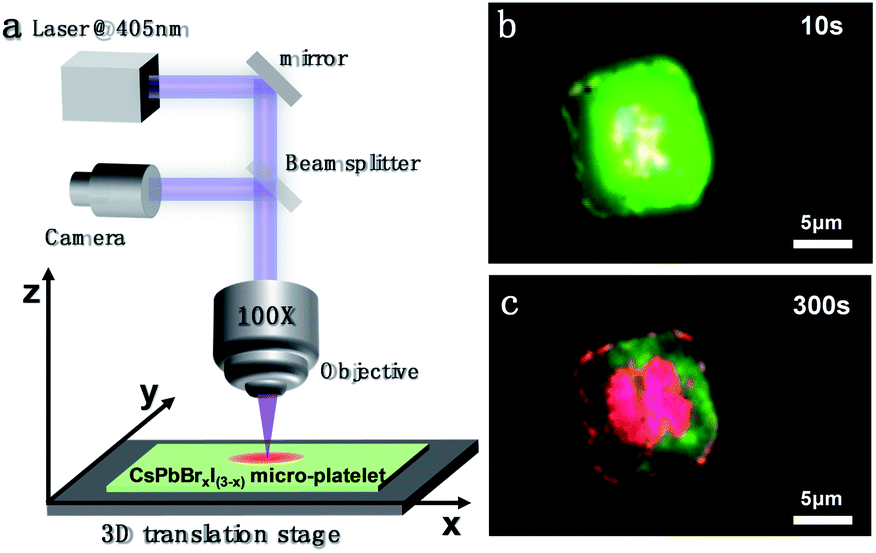 | ||
| Fig. 6 Schematic diagram of preparation of a photo-pattern. (a) A schematic diagram of the optical configuration of the laser irradiation. (b and c) Fluorescence micrographs of the individual CsPbBrxI(3−x) micro-platelet moving along the square path for 10 s and 300 s under laser irradiation and the scale bar is 5 μm. | ||
Conclusions
In summary, we have fabricated all-inorganic CsPbBrxI(3−x) single crystals by the CVD method and investigated the laser irradiation induced real-time IM process with the corresponding PL spectra in the samples. We revealed that the local electric field is the driving force for IM and confirmed this by applying a bias to an ITO/perovskite/ITO configuration. By comparing the PL and the PL decay curves of the CsPbBrxI(3−x) micro-platelet with and without PMMA, we proved that the vacancies on the single crystal surface are the main movement pathway. Understanding the path of IM in CsPbBrxI(3−x) single crystal micro-platelets is of great importance since it can provide knowledge for the development of perovskite materials with improving stability and for further applications.Experimental
Fabrication of CsPbBrxI(3−x) micro-platelets
The CsPbBrxI(3−x) micro-platelets were fabricated by the chemical vapor deposition method. The mica substrate was placed inside the downstream of a quartz tube. To prepare the precursors, we mixed the PbBr2 powder and CsI powder with a molar ratio of 1![[thin space (1/6-em)]](https://www.rsc.org/images/entities/char_2009.gif) :1 and placed it in the heating area. Then the whole system was pumped down to 10 Pa, which was followed by a 205 sccm flow of high purity Ar (99.99%) passing through the tube until the atmospheric pressure was achieved. Afterwards, the reaction was carried out at atmospheric pressure accompanied by a continuous 30 sccm flow of high purity Ar. The reaction temperature was set at 570 °C and held for 20 min.
:1 and placed it in the heating area. Then the whole system was pumped down to 10 Pa, which was followed by a 205 sccm flow of high purity Ar (99.99%) passing through the tube until the atmospheric pressure was achieved. Afterwards, the reaction was carried out at atmospheric pressure accompanied by a continuous 30 sccm flow of high purity Ar. The reaction temperature was set at 570 °C and held for 20 min.
Optical characterization
PL measurements were performed using a home-made micro-area fluorescence test system with a 405 nm laser source. The laser beam was focused and pumped on the selected area of perovskite by a microscope objective. Both the optical micrograph in bright field and the laser-irradiated fluorescence micrograph in dark field were taken using the same color camera. The time-resolved fluorescence decay curves were measured by replacing the 405 nm laser with a 375 nm pulsed laser (5 MHz) in the same test system and detected using a single photon counting photomultiplier module (id 100).Atomic force microscopy (AFM) images
AFM measurements were conducted using a Bruker Multimode 8 test system. All measurements were performed in the Scanasyst-Air mode with silicon tips on a nitride lever from Bruker.Scanning electron microscopy (SEM) images
SEM images were recorded on an FEI Quanta 250F field emission environment scanning electron microscope.Conflicts of interest
There are no conflicts to declare.Acknowledgements
This work was supported by the Natural Science Foundation of Jiangsu Province (BK20190446) and NSFC (11904172). Y. W acknowledges the support of the One-Thousand Talent Programs from Chinese Government and the start-up funding from Nanjing University of Science and Technology.Notes and references
- J. Song, J. Li, X. Li, L. Xu, Y. Dong and H. Zeng, Adv. Mater., 2015, 27, 7162–7167 CrossRef CAS PubMed.
- X. Li, Y. Wang, H. Sun and H. Zeng, Adv. Mater., 2017, 29, 1701185 CrossRef PubMed.
- Y. Wang, X. Li, J. Song, L. Xiao, H. Zeng and H. Sun, Adv. Mater., 2015, 27, 7101–7108 CrossRef CAS PubMed.
- J. Song, Q. Cui, J. Li, J. Xu, Y. Wang, L. Xu, J. Xue, Y. Dong, T. Tian, H. Sun and H. Zeng, Adv. Opt. Mater., 2017, 5, 1700157 CrossRef.
- J. Ding, S. Du, Z. Zuo, Y. Zhao, H. Cui and X. Zhan, J. Phys. Chem. C, 2017, 121, 4917–4923 CrossRef CAS.
- N. E. Chart, https://www.nrel.gov/pv/cell-efficiency.html, 2019.
- Y. Yuan and J. Huang, Acc. Chem. Res., 2016, 49, 286–293 CrossRef CAS PubMed.
- C. Li, S. Tscheuschner, F. Paulus, P. E. Hopkinson, J. Kiessling, A. Kohler, Y. Vaynzof and S. Huettner, Adv. Mater., 2016, 28, 2446–2454 CrossRef CAS PubMed.
- T. Duong, H. K. Mulmudi, Y. Wu, X. Fu, H. Shen, J. Peng, N. Wu, H. T. Nguyen, D. Macdonald, M. Lockrey, T. P. White, K. Weber and K. Catchpole, ACS Appl. Mater. Interfaces, 2017, 9, 26859–26866 CrossRef CAS PubMed.
- D. A. Jacobs, Y. Wu, H. Shen, C. Barugkin, F. J. Beck, T. P. White, K. Weber and K. R. Catchpole, Phys. Chem. Chem. Phys., 2017, 19, 3094–3103 RSC.
- P. Liu, W. Wang, S. Liu, H. Yang and Z. Shao, Adv. Energy Mater., 2019, 9, 1803017 CrossRef.
- A. Sadhanala, F. Deschler, T. H. Thomas, S. E. Dutton, K. C. Goedel, F. C. Hanusch, M. L. Lai, U. Steiner, T. Bein, P. Docampo, D. Cahen and R. H. Friend, J. Phys. Chem. Lett., 2014, 5, 2501–2505 CrossRef CAS PubMed.
- S. D. Stranks, G. E. Eperon, G. Grancini, C. Menelaou, M. J. P. Alcocer, T. Leijtens, L. M. Herz, A. Petrozza and H. J. Snaith, Science, 2013, 342 Search PubMed.
- Q. Dong, Y. Fang, Y. Shao, P. Mulligan, J. Qiu, L. Cao and J. Huang, Science, 2015, 347, 967–970 CrossRef CAS PubMed.
- D. W. deQuilettes, S. M. Vorpahl, S. D. Stranks, H. Nagaoka, G. E. Eperon, M. E. Ziffer, H. J. Snaith and D. S. Ginger, Science, 2015, 348, 683–686 CrossRef CAS PubMed.
- E. T. Hoke, D. J. Slotcavage, E. R. Dohner, A. R. Bowring, H. I. Karunadasa and M. D. McGehee, Chem. Sci., 2015, 6, 613–617 RSC.
- H. Zhang, X. Fu, Y. Tang, H. Wang, C. Zhang, W. W. Yu, X. Wang, Y. Zhang and M. Xiao, Nat. Commun., 2019, 10, 1088 CrossRef PubMed.
- S. Meloni, T. Moehl, W. Tress, M. Franckevicius, M. Saliba, Y. H. Lee, P. Gao, M. K. Nazeeruddin, S. M. Zakeeruddin, U. Rothlisberger and M. Graetzel, Nat. Commun., 2016, 7, 10334 CrossRef CAS PubMed.
- S. Draguta, O. Sharia, S. J. Yoon, M. C. Brennan, Y. V. Morozov, J. S. Manser, P. V. Kamat, W. F. Schneider and M. Kuno, Nat. Commun., 2017, 8, 200 CrossRef PubMed.
- A. J. Barker, A. Sadhanala, F. Deschler, M. Gandini, S. P. Senanayak, P. M. Pearce, E. Mosconi, A. J. Pearson, Y. Wu, A. R. Srimath Kandada, T. Leijtens, F. De Angelis, S. E. Dutton, A. Petrozza and R. H. Friend, ACS Energy Lett., 2017, 2, 1416–1424 CrossRef CAS.
- A. F. Gualdron-Reyes, S. J. Yoon, E. M. Barea, S. Agouram, V. Munoz-Sanjose, A. M. Melendez, M. E. Nino-Gomez and I. Mora-Sero, ACS Energy Lett., 2019, 4, 54–62 CrossRef CAS PubMed.
- A. J. Knight, A. D. Wright, J. B. Patel, D. P. McMeekin, H. J. Snaith, M. B. Johnston and L. M. Herz, ACS Energy Lett., 2018, 4, 75–84 CrossRef.
- C. G. Bischak, C. L. Hetherington, H. Wu, S. Aloni, D. F. Ogletree, D. T. Limmer and N. S. Ginsberg, Nano Lett., 2017, 17, 1028–1033 CrossRef CAS PubMed.
- Q. Dong, J. Song, Y. Fang, Y. Shao, S. Ducharme and J. Huang, Adv. Mater., 2016, 28, 2816–2821 CrossRef CAS PubMed.
- M. Kulbak, D. Cahen and G. Hodes, J. Phys. Chem. Lett., 2015, 6, 2452–2456 CrossRef CAS PubMed.
- L. Protesescu, S. Yakunin, M. I. Bodnarchuk, F. Krieg, R. Caputo, C. H. Hendon, R. X. Yang, A. Walsh and M. V. Kovalenko, Nano Lett., 2015, 15, 3692–3696 CrossRef CAS PubMed.
- C. Ran, J. Xu, W. Gao, C. Huang and S. Dou, Chem. Soc. Rev., 2018, 47, 4581–4610 RSC.
- C. Huo, X. Liu, X. Song, Z. Wang and H. Zeng, J. Phys. Chem. Lett., 2017, 8, 4785–4792 CrossRef CAS PubMed.
- W. Mao, C. R. Hall, A. S. R. Chesman, C. Forsyth, Y. B. Cheng, N. W. Duffy, T. A. Smith and U. Bach, Angew. Chem., Int. Ed. Engl., 2019, 58, 2893–2898 CrossRef CAS.
- D. W. deQuilettes, W. Zhang, V. M. Burlakov, D. J. Graham, T. Leijtens, A. Osherov, V. Bulovic, H. J. Snaith, D. S. Ginger and S. D. Stranks, Nat. Commun., 2016, 7, 11683 CrossRef CAS PubMed.
- Y. Wang, Y. Ren, S. Zhang, J. Wu, J. Song, X. Li, J. Xu, C. H. Sow, H. Zeng and H. Sun, Commun. Phys., 2018, 1, 96 CrossRef.
- M. C. Brennan, S. Draguta, P. V. Kamat and M. Kuno, ACS Energy Lett., 2017, 3, 204–213 CrossRef.
- W.-K. Hong, B.-J. Kim, T.-W. Kim, G. Jo, S. Song, S.-S. Kwon, A. Yoon, E. A. Stach and T. Lee, Colloids Surf., A, 2008, 313–314, 378–382 CrossRef.
- Y. Gao and X. Peng, J. Am. Chem. Soc., 2015, 137, 4230–4235 CrossRef CAS.
Footnote |
| † Electronic supplementary information (ESI) available: EDX mapping of two CsPbBrxI(3−x) micro-platelets. AFM measurements of CsPbBrxI(3−x) micro-platelets. Normalized PL spectra. Optical measurements of another sample. PL spectra of an individual CsPbBrxI(3−x) micro-platelet fabricated by using PbBr2 and CsI precursor powders with a molar ratio of 1:2. PL intensity change of samples with and without PMMA. See DOI: 10.1039/c9na00565j |
| This journal is © The Royal Society of Chemistry 2019 |