
 Open Access Article
 This Open Access Article is licensed under a Creative Commons Attribution-Non Commercial 3.0 Unported Licence
Evidence of a strong perpendicular magnetic anisotropy in Au/Co/MgO/GaN heterostructures†
Xue
Gao
abc,
Baishun
Yang
d,
Xavier
Devaux
b,
Hongxin
Yang
d,
Jianping
Liu
ac,
Shiheng
Liang
b,
Mathieu
Stoffel
b,
Ludovic
Pasquier
b,
Bérangère
Hyot
e,
Adeline
Grenier
e,
Nicolas
Bernier
e,
Sylvie
Migot
b,
Stéphane
Mangin
b,
Hervé
Rinnert
b,
Chunping
Jiang
ac,
Zhongming
Zeng
 ac,
Ning
Tang
f,
Qian
Sun
ac,
Sunan
Ding
ac,
Hui
Yang
ac and
Yuan
Lu
*b
ac,
Ning
Tang
f,
Qian
Sun
ac,
Sunan
Ding
ac,
Hui
Yang
ac and
Yuan
Lu
*b
aSchool of Nano Technology and Nano Bionics, University of Science and Technology of China, 96 Jinzhai Road, Baohe, Hefei 230026, P. R. China
bUniversité de Lorraine, CNRS, Institut Jean Lamour, UMR 7198, campus ARTEM, 2 Allée André Guinier, 54011 Nancy, France. E-mail: yuan.lu@univ-lorraine.fr
cKey Laboratory of Nanodevices and Applications, Suzhou Institute of Nano-Tech and Nano-Bionics, Chinese Academy of Sciences, Suzhou 215123, P. R. China
dKey Laboratory of Magnetic Materials and Devices, Ningbo Institute of Materials Technology and Engineering, Chinese Academy of Sciences, Ningbo 315201, P. R. China
eUniv. Grenoble-Alpes, CEA, Leti, F-38000 Grenoble, France
fSchool of Physics, Peking University, 100871, Beijing, P. R. China
First published on 30th September 2019
Abstract
We report a strong perpendicular magnetic anisotropy (PMA) in Au/Co/MgO/GaN heterostructures from both experiments and first-principles calculations. The Au/Co/MgO heterostructures have been grown by molecular beam epitaxy (MBE) on GaN/sapphire substrates. By carefully optimizing the growth conditions, we obtained a fully epitaxial structure with a crystalline orientation relationship Au(111)[![[1 with combining macron]](https://www.rsc.org/images/entities/char_0031_0304.gif) 10]//Co(0001)[11
10]//Co(0001)[11![[2 with combining macron]](https://www.rsc.org/images/entities/char_0032_0304.gif) 0]//MgO(111)[10]//GaN(0002)[110]. More interestingly, we demonstrate that a 4.6 nm thick Co film grown on MgO/GaN still exhibits a large perpendicular magnetic anisotropy. First-principles calculations performed on the Co (4ML)/MgO(111) structure showed that the MgO(111) surface can strongly enhance the magnetic anisotropy energy by 40% compared to a reference 4ML thick Co hcp film. Our layer-resolved and orbital-hybridization resolved anisotropy analyses helped to clarify that the origin of the PMA enhancement is due to the interfacial hybridization of O 2p and Co 3d orbitals at the Co/MgO interface. The perpendicularly magnetized Au/Co/MgO/GaN heterostructures are promising for efficient spin injection and detection in GaN based opto-electronics without any external magnetic field.
0]//MgO(111)[10]//GaN(0002)[110]. More interestingly, we demonstrate that a 4.6 nm thick Co film grown on MgO/GaN still exhibits a large perpendicular magnetic anisotropy. First-principles calculations performed on the Co (4ML)/MgO(111) structure showed that the MgO(111) surface can strongly enhance the magnetic anisotropy energy by 40% compared to a reference 4ML thick Co hcp film. Our layer-resolved and orbital-hybridization resolved anisotropy analyses helped to clarify that the origin of the PMA enhancement is due to the interfacial hybridization of O 2p and Co 3d orbitals at the Co/MgO interface. The perpendicularly magnetized Au/Co/MgO/GaN heterostructures are promising for efficient spin injection and detection in GaN based opto-electronics without any external magnetic field.
1. Introduction
III-nitride semiconductors have wide applications in display, optical data storage, ultraviolet detectors and high-power high-frequency electronic devices.1–4 GaN is also an attractive candidate for spintronic applications since it has a weak spin–orbit interaction (Δso ≈ 15 meV)5 combined with a wide band gap (∼3.4 eV) at 300 K. This leads to a long spin relaxation time (∼20 ns at 5 K and a few hundred ns at room temperature),6 which is three orders of magnitude higher than the spin lifetime of GaAs (about 500 ps at 10 K).7,8 The long spin coherence time provides an important advantage for GaN applications in semiconductor spintronic devices. The most important semiconductor spintronic devices are spin light emitting diodes (spin-LED) and spin lasers. These types of devices consist of two parts: the ferromagnetic layer (spin-injector) which is used to inject spin-polarized electrons and the semiconductor part which is used to emit light. The injected spin-polarized electrons from the spin-injector recombine with the unpolarized holes in the semiconductor active region to emit circularly polarized light.9–15 Potential devices have been proposed based on this advanced semiconductor technology, ranging from memory elements with optical readout and optical transport of spin information,16 advanced optical switches,17 circularly polarized single photon emitters for quantum cryptography18 to medical chiral analysis,19 and three-dimensional (3D) display screens.20 Recently, results of GaN-based visible spin-LED and spin lasers have been reported.21,–27 Circular polarizations of ∼6% (ref. 25) and ∼25% (ref. 26) have been demonstrated for GaN based spin LED and spin polariton diode lasers at room temperature (RT), respectively. This paves the way for the development of III-nitride based spin opto-electronics.In the applications of spin-LED and spin lasers with surface emission geometries, such as 3D displays, the actually used spin injector (GaMnN,21,22 GaCrN,23 Fe3O4,24,27 and CoFe25,26) with in-plane magnetization anisotropy is not possible for practical application. This is because, according to the optical selection rules,28 the magnetization of the spin injector has to be maintained perpendicular to the quantum-well (QW) LED surface in order to emit circularly polarized light from the surface. If the spin injector has an in-plane magnetization, a strong external magnetic field of up to several Tesla is required to rotate the magnetization perpendicular to the grown layers. For practical applications, it is important to realize remnant circular polarization at zero or at small magnetic fields. For this reason, the development of spin injectors exhibiting perpendicular magnetic anisotropy (PMA) is indispensable.11,12,14,15
In this work, we have demonstrated a strong perpendicular magnetic anisotropy in Au/Co/MgO/GaN heterostructures from both experiments and first-principles calculations. The Au/Co/MgO heterostructures have been epitaxially grown by molecular beam epitaxy (MBE) on GaN/sapphire substrates. A systematic study of interfacial structures and chemistry has been performed by high resolution scanning transmission electron microscopy (HR-STEM) combined with electron energy-loss spectroscopy (EELS). We show that a 4.6 nm thick Co film grown on MgO/GaN still exhibits a large PMA up to room temperature. First-principles calculations have been performed to understand the origin of large PMA in the Au/Co/MgO/GaN heterostructures.
2. Experimental methods
In our experiments, an epitaxial 2 μm-thick GaN (0001) layer was first grown on a c-plane sapphire (Al2O3) substrate by metal–organic chemical vapor deposition (MOCVD). Then the GaN/sapphire substrate was transferred through air to a molecular beam epitaxy (MBE) chamber (with a base pressure of 1 × 10⁻¹⁰ torr) to continue the growth of the Au/Co/MgO structure. To remove both the native oxide layer and possible surface contaminants, we dipped the sample in 10% HCl solution for 5 min. After loading the sample into the MBE chamber, an in situ deoxidation is further performed by heating the sample to 600 °C for 30 min. Then, a 3 nm thick MgO film was deposited by e-beam evaporation on the GaN surface kept at 200 °C. The MgO layer serves as a tunneling barrier to overcome the impedance mismatch problem for spin injection from a ferromagnetic metal to a semiconductor.29 The growth of a 5 nm thick Co layer on MgO was then performed at RT, followed by annealing at 250 °C for 20 min to improve the crystalline quality. Finally, a 5 nm thick Au layer was grown on the top of the Co/MgO/GaN heterostructure to protect the sample from oxidation. The schematic of the layer structure is shown in Fig. 1(a). The quality of the growing layers was monitored by in situ reflection high energy electron diffraction (RHEED) measurements with the incident electron beam being accelerated at 30 kV.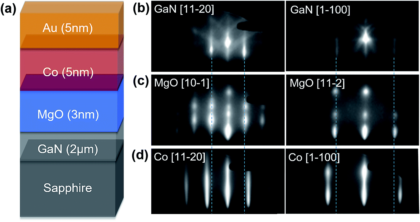 | ||
| Fig. 1 (a) Schematic diagram of the Au/Co/MgO/GaN heterostructure. In situ RHEED patterns taken at 30 kV beam energy along the [110] and [100] azimuths of GaN for (b) GaN surface after deoxidation at 600 °C, (c) after 3 nm MgO deposition at RT and (d) after 5 nm Co deposition and annealing at 250 °C. The blue dashed lines help to compare the streak spacing between different layers. The epitaxial relationship is found to be Co[110]//MgO[10]//GaN[110] and Co[100]//MgO[11]//GaN[100]. | ||
High-resolution transmission electron microscopy (HR-TEM) and HR-STEM combined with spatially resolved EELS were performed by using a probe-corrected FEI TITAN and a probe-corrected microscope JEOL ARM200F equipped with a GATAN GIF quantum energy filter to reveal the structure and element distribution in the Au/Co/MgO/GaN heterostructure. The microscopes were operated at 200 kV. High angle annular dark-field (HAADF), annular dark-field (ADF) and bright-field (BF) images were simultaneously recorded for the structural study, while only HAADF and ADF signals were recorded during EELS chemical analysis. Two EELS spectrum images were simultaneously recorded with an energy dispersion of 0.5 eV, one containing the zero and low loss peaks and the other one containing the high loss peaks. EELS spectrum images were denoised using a principal component analysis procedure30 before their processing to draw the chemical maps. More details on EELS processing can be found in ESI note 2.† A thin lamella for STEM investigations was prepared by focused ion beam milling. During this procedure the sample is capped by a Pt–C layer on the area of lift out. This layer appears in TEM or STEM micrographs as granular Pt–C deposited on the Au layer. Ex situ magnetic measurements were performed using a superconducting quantum interference device (SQUID) and vibrating sample magnetometer (VSM).
3. Results and discussion
3.1 In situ and ex situ structural characterization of Au/Co/MgO/GaN heterostructures
Fig. 1(b) shows the RHEED patterns from the GaN surface along both [110] and [100] azimuthal directions after in situ deoxidation at 600 °C. The streaky patterns with faint Kikuchi lines indicate a high quality, smooth and long range ordered GaN (0001) surface. We then deposit a 3 nm thick MgO layer at 200 °C on the GaN surface. This growth temperature has been optimized to get the best crystallinity and lowest surface roughness (see details in ESI note 1†). Although the RHEED patterns obtained after MgO growth become spotty (Fig. 1(c)), they are compatible with the patterns obtained after GaN deoxidation in both azimuthal directions. Moreover, the patterns repeat every 60°, thus indicating an epitaxial growth relationship between MgO and GaN. As reported by Craft et al.,31 there are two possible orientations for the growth of a rock salt-structure MgO on a wurtzite-structure GaN. One possibility is that the MgO [110] direction is parallel to the GaN [110] direction. In this case, a lattice mismatch of about 6.9% is obtained between MgO and GaN and the MgO layer is tensile strained. The other possibility is that the MgO [110] direction is parallel to the GaN [100] direction. In this case, a lattice mismatch of about 7.4% is obtained between MgO and GaN and the MgO layer is compressively strained. The two orientations are degenerated from the point of view of the surface energy and it is difficult to predict the chemically preferred orientation. From our RHEED patterns, the spacing between the diffraction streaks of MgO is slightly larger than that of GaN (see blue dashed lines in Fig. 1(c)), indicating a smaller lattice constant of MgO compared to that of GaN, which corresponds well to the first orientation relationship: MgO(111) [10]//GaN(0001) [110].
The growth of a 5 nm thick Co film on MgO is performed at RT to ensure a full coverage of Co on MgO due to the well-known wetting problem of metals on oxides. The as-grown Co film is characterized by an elongated spot-like RHEED pattern (not shown). However, the pattern becomes streaky after annealing at 250 °C for 20 min, indicating an improvement of both surface roughness and crystallinity (Fig. 1(d)). As marked by the blue dotted lines in Fig. 1(d), the separation between the diffraction streaks is larger for Co than for MgO thus indicating that Co has a smaller lattice constant. From the RHEED observations, we can thus deduce the epitaxial orientation relationship which is given using Co(0001)[110]//MgO(111)[10]. This is quite surprising since the lattice mismatch corresponding to this epitaxial relationship is as large as 16%. Nevertheless, our finding is consistent with the epitaxial relationship reported by Nukaga et al.32
HR-STEM has been used to investigate the interfacial structure of the Au/Co/MgO/GaN heterostructure. In Fig. 2(a), the low magnification bright-field STEM image reveals a good homogeneity and low roughness of the heterostructure. From the high magnification STEM image of the cross section (Fig. 2(b)), the real thickness of MgO and Co can be measured to be 2.9 nm and 4.6 nm, respectively. MgO appears well crystalline and with epitaxial relationships with GaN. This confirms what was observed by RHEED during the sample growth. The analysis of the patterns obtained by the fast Fourier transform (FFT) of the HR-STEM images has confirmed the orientation relationship between MgO and GaN and between Co and MgO that was already described in the above RHEED analysis. Because of the strong difference of mean atomic numbers between the layers, there are large differences of electron diffusion between the different layers. It is thus difficult to show atomic arrangements of all layers in one STEM image due to the limited contrast. To more easily display the atomic plane spacing in all layers and precisely define the interfaces, the contrast between layers was equalized and an intensity profile perpendicularly crossing the interfaces was drawn from a HAADF micrograph (Fig. 2(c)). Each peak can be identified with one atomic plane. From the left to the right, GaN, MgO, Co and Au can be identified. The GaN/MgO interface is found to be very sharp. However, the interface between MgO and Co seems to be more difficult to define from the atomic plane spacing and from the contrast variation in the HAADF image. Red dotted lines on Fig. 2(c) show the location of this interface where the phase is not clear on a 2 or 3 atomic plane thickness range corresponding to 0.5–0.7 nm. Two possibilities could explain this observation. The first could have its origin in the roughness on the surface of the MgO layer. Since the TEM lamella has a certain thickness, a small interface roughness can result in the superposition of MgO and Co without any break in the epitaxial relationship. However, this possibility can be excluded from the measurement of MgO surface roughness, which shows an atomic step feature with room mean square roughness of about 2.4 Å (see ESI note 1†). The other reason could be the reaction between MgO and Co at the interface, inducing the oxidation of Co or the formation of a mixed oxide at the interface.
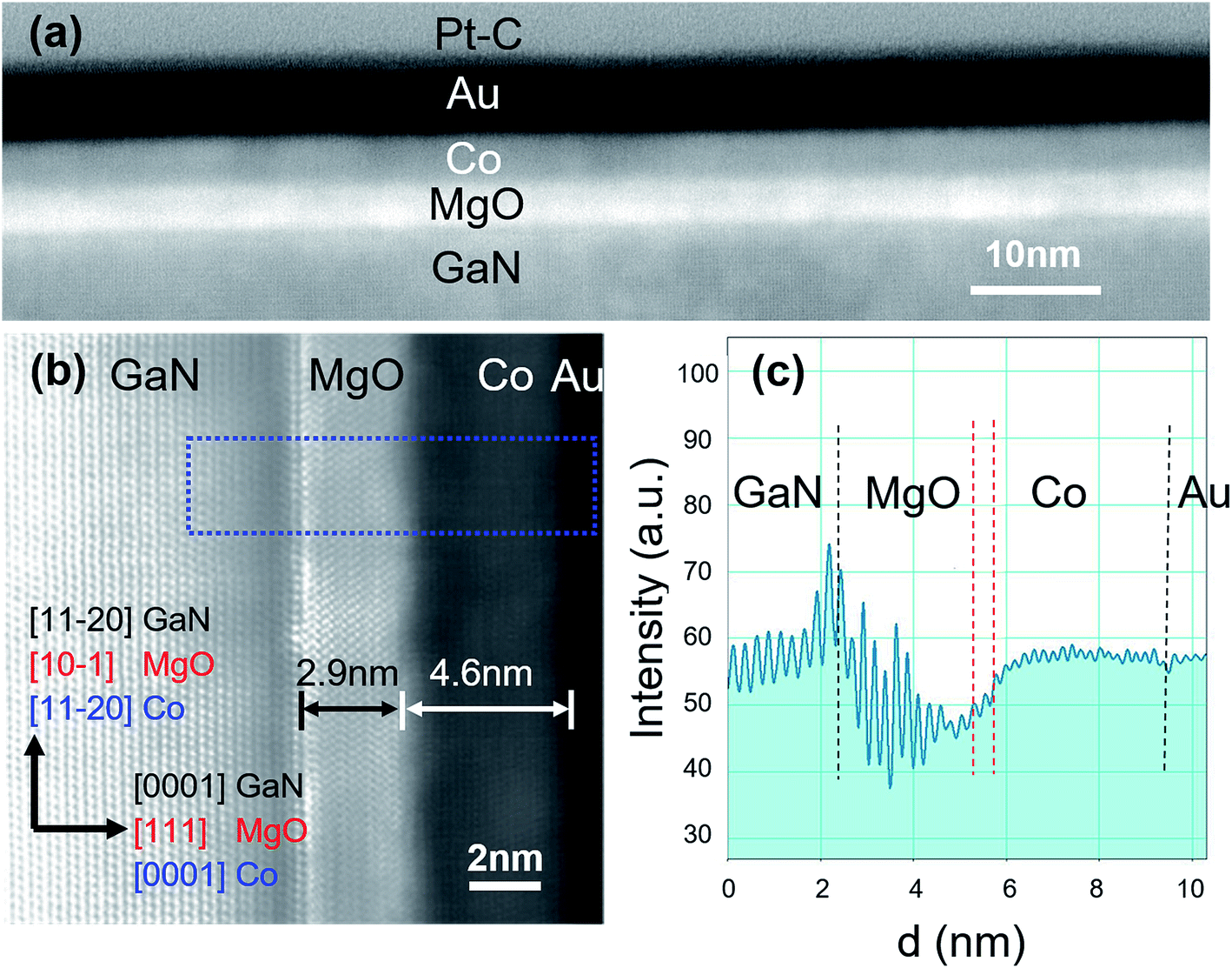 | ||
| Fig. 2 (a) Large-scale cross-sectional HR-STEM dark field image of the Au/Co/MgO/GaN interface. PtC capping was deposited during the lamella processing by FIB. (b) Magnified HR-STEM bright field image showing the detailed structure at the GaN/MgO/Co interface. (c) Intensity profile drawn from the equalized HAADF image recorded in the rectangular area (marked with blue dashed lines in panel (b)). The peaks indicate the position of atom planes, showing from left to right GaN (0002)//MgO (111)//Co (0002)//Au (111). The two red lines indicate the zone where a “gray” contrast at the MgO/Co interface revealing a possible chemical reaction between MgO and Co. | ||
To understand the chemistry distribution of this interface, spatially resolved STEM-EELS analyses were performed. Fig. 3(a) shows a HAADF image of the area where EELS spectrum images were recorded. Typical EELS spectra of the different layers are shown in ESI note 2.†Fig. 3(b) shows elemental maps extracted from the semi-quantitative analysis of the EELS spectrum images. The maps drawn respectively from NK, MgL23, OK, CoL3, and AuN45 edges clearly display the distribution of the different elements in the Au/Co/MgO/GaN heterostructure. To qualitatively identify the interface diffusion, semi-quantitative profiles of the elements are plotted in Fig. 3(c). Each point in the profile is extracted by integrating the elemental signals of the EELS maps from an area of 0.2 nm in height (about 1 atomic column) and 10 nm in width parallel to the interfaces. Some information can be obtained from these profiles. First, at the Co/Au interface, the overlap of Co and Au seems large, indicating a notable inter-diffusion of Co and Au at this interface. This agrees with the inter-diffusion between Co and Au that has been observed in organic spin valve structures when the Co/Au layers are grown at room temperature.33 Second, we can observe a separation of about 0.4 nm between the slopes of Mg and O signals at the MgO/Co interface. This slope separation and the small overlapping of the Co signal with Mg and O signals indicate the oxidation of cobalt at the interface and the possible formation of a MgxCoyOz mixed oxide layer with a thickness of 2–3 atomic layers. This explains the reason why a diffusive contrast is observed at the MgO/Co interface in the HR-TEM or HR-STEM images. Third, a structurally sharp and chemically clean GaN/MgO interface is confirmed even after annealing treatment at 600 °C.
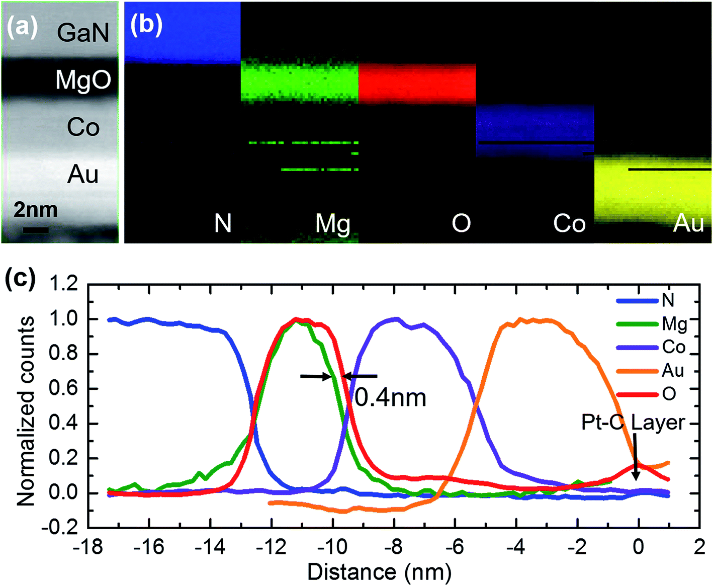 | ||
| Fig. 3 (a) HAADF image recorded simultaneously with the EELS spectrum images. The GaN substrate is presented on the top of the image. (b) Individual element maps drawn with NK, MgL23, OK, CoL3, and AuN45 signals extracted from processed EELS spectrum images. (c) The normalized profiles of elements were extracted from the maps of elements. | ||
3.2 Magnetic properties of Co(0001)/MgO(111)
The magnetic properties of the Au(5 nm)/Co(4.6 nm)/MgO(2.9 nm)/GaN sample have been measured using a SQUID and VSM. Fig. 4(a) shows the magnetic hysteresis loops acquired using a SQUID at RT with both in-plane (IP) and out-of-plane (OOP) applied magnetic fields. A clear perpendicular magnetic anisotropy can be observed since the remnant magnetization at zero field in out-of-plane measurements is much larger than that obtained for the in-plane measurements. The ratio of perpendicular remnant magnetization to the saturation magnetization (MR/MS) reaches about 0.8 at room temperature. To confirm that the in-plane measurements are not influenced by the in-plane magnetic hard axis, we have performed measurements of in-plane remnant magnetization as a function of in-plane angle with a magnetic field using a VSM, as shown in Fig. 4(b). We have observed a uniaxial behavior with the maximum of MR/MS not exceeding 0.2. Thus, the large perpendicular magnetic anisotropy is confirmed in our sample. We can further extract the effective anisotropy constant (Keff) by calculating the difference in area between the magnetization loops measured when the magnetic field is applied perpendicular and parallel to the layers. The Keff is extracted to be 2.2 × 10⁵ J m−3 at RT (see details in ESI note 3†). The inset of Fig. 4(a) shows the hysteresis loops measured at different temperatures with an out-of-plane field. The coercivity and MR/MS increase with the decrease of temperature, indicating an improvement of PMA at low temperatures.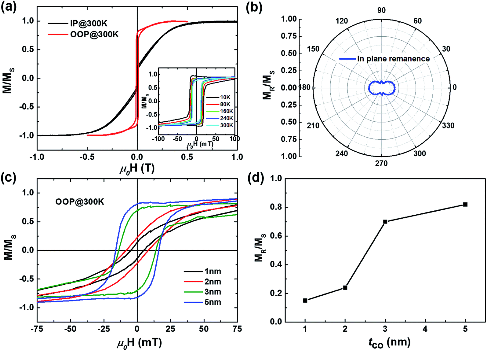 | ||
| Fig. 4 (a) M–H curves measured at RT using a SQUID for the Co (4.6 nm)/MgO/GaN structure with applied in-plane (IP) and out-of-plane (OOP) magnetic fields. Inset: M–H curves at different temperatures with an OOP field. (b) Normalized in-plane remnant magnetization as a function of in-plane angle with a magnetic field. (c) RT out-of-plane M–H curves for Co/MgO/GaN with different Co thicknesses. (d) Normalized perpendicular remnant magnetization as a function of different Co thicknesses. | ||
This observed large PMA is quite surprising for such a thick Co layer (4.6 nm) since the bulk in-plane anisotropy and demagnetization always tend to keep the magnetization in-plane. This thickness is much larger than that of the intensively studied Fe (1.2 nm)/MgO structure11,34 and almost twice as large as the recent reported Co thickness (2.5 nm) on graphene.35 Since the PMA at the Au/Co interface has already been published,36–39 it is important to verify if the observed large PMA in our Au/Co/MgO/GaN heterostructures originates from the Au/Co interface. We have designed two control samples to clarify the origin of PMA. One sample has the structure of GaN//MgO(2.9 nm)/Co(4.6 nm)/MgO(5 nm)/MgAlOx(2 nm), i.e. without the coverage of Au. Fig. S4 (see in the ESI†) shows the M–H loop measured at RT with an out-of-plane magnetic field. The sample shows an evident perpendicular magnetic anisotropy with a MR/MS ratio of 0.64 and coercivity of 700 Oe which is slightly different from our sample with Au coverage. This could be due to the increase of effective magnetic layers due to the suppression of inter-diffusion at the Au/Co interface. The second sample has the structure of GaN//Au(5 nm)/Co(4.6 nm)/Au(5 nm), i.e. replacing MgO by a Au underlayer. The results (Fig. S6 (see in the ESI†)) clearly show a clear in-plane anisotropy with almost zero remanence of magnetization for the out-of-plane curve. Furthermore, since our TEM results have revealed that an inter-diffusion exists at the Au/Co interface, the contribution of PMA from the diffused Au/Co interface should be very small because a sharp interface is necessary to generate the PMA.39 Therefore, we can conclude that the observed large PMA should be mainly due to the contribution from the Co/MgO interface. Neither a Au/Co interface nor a Co bulk contribution can give a sizable PMA in our Au/Co/MgO/GaN system. Please see more discussion in ESI note 4.†
To understand the interface contribution to the establishment of PMA, we have prepared several Au/Co/MgO/GaN samples with different thicknesses of Co varying from 1 to 5 nm. Fig. 4(c) shows the hysteresis loops measured at RT with an out-of-plane magnetic field. It is found that the PMA cannot be established for thin Co thicknesses (lower than 3 nm). Moreover, the ratio MR/MS increases with the increase of Co thickness (Fig. 4(d)). This can be understood as due to an incomplete coverage of the Co layer on the MgO surface when the Co layer is too thin. As reported for the growth of Co on the MgO(100) surface,40,41 a 2 nm thick Co layer grows by following the Volmer–Weber growth mode (3D island formation), while a 5 nm thick Co thickness can form a continuous film on MgO. Therefore, the magnetic properties of very thin Co films are dominated by the superparamagnetic behavior of Co islands.40 Each Co island has its own magnetization, and its magnetization direction can be randomly flipped under the influence of temperature. In the absence of an external magnetic field, the average magnetization is zero and no remnant magnetization can be measured. Therefore, PMA cannot be established in the superparamagnetic Co islands due to the strong influence of temperature. For Co thicknesses larger than 3 nm, the PMA can be then established when the film becomes continuous and ferromagnetic.
3.3 First-principles calculations of Co(0001)/MgO(111)
To further shed light on the origin of the perpendicular magnetic anisotropy from the Co/MgO interface, we performed first-principles calculations with the Vienna ab initio simulation package (VASP).42–44 In all calculations, the exchange–correlation potentials were treated with the generalized gradient approximation (GGA) using the Perdew–Burke–Ernzerhof (PBE) function.45 The cutoff energy is 420 eV and a 9 × 9 × 1 k-mesh was used in the calculations. The convergence energy and force of the heterostructure are 10−7 eV and 0.001 eV Å−1, respectively. The optimized 4 monolayer (ML) Co(0001)/MgO(111) structure is shown in Fig. 5(a) for the side view and in Fig. 5(b) for the top view. The magnetic anisotropy energy (MAE) is defined as MAE = Ex − Ez, where Ex and Ez are energies corresponding to magnetic moments aligned along in-plane and out-of-plane orientations, respectively. In this definition, a positive MAE corresponds to a perpendicular magnetic anisotropy.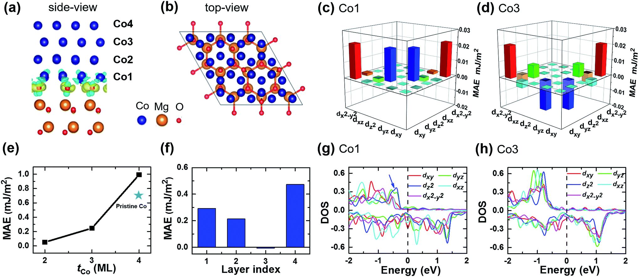 | ||
| Fig. 5 (a) Side view of the calculated Co (4ML)/MgO (111) structure. At the Co/MgO interface, the yellow and sky blue colors represent the charge accumulation and depletion regions, respectively. The isosurface charge density is 0.01 e Å−3. (b) Top view of Co on the MgO (111) surface. Orbital-resolved MAE of selected (c) Co1 and (d) Co3 in the Co (4ML)/MgO structure. (e) Calculated MAE as a function of Co thickness. (f) Layer-resolved MAE in the Co(4ML)/MgO structure. Project density of states of selected (g) Co1 and (h) Co3 atoms in the Co (4ML)/MgO structure. | ||
The calculated MAE as a function of Co thickness ranging from 2 to 4 MLs is shown in Fig. 5(e). It is shown that the MAE increases as the Co thickness increases. For 4 MLs of Co on MgO, the PMA can reach up to 0.99 mJ m−2. For comparison, we have also calculated the MAE of a pristine 4ML thick Co layer as a reference, whose MAE is equal to 0.71 mJ m−2. Therefore, the growth of Co on MgO (111) leads to a 40% enhancement of PMA compared to the pristine Co layer. The contribution of PMA is further analyzed from the layer-resolved MAE for the Co(4ML)/MgO structure, as shown in Fig. 5(f). Similar to the Fe/MgO heterostructure,11,46,47 the interfacial (Co1) and surface (Co4) Co atoms dominate the PMA, while the MAE of the third layer of Co is negative, which indicates an in-plane anisotropy. The positive MAE for the surface Co atoms is due to the surface effect. To comprehensively understand the enhancement of MAE for the interfacial Co, we have performed a comparison between Co at the interface (Co1) and Co in the third layer (Co3) in the form of orbital resolved MAE, as shown in Fig. 5(c) and (d), respectively. One can see that the matrix element of (dxy, dx2−y2) (denoted as red bars in Fig. 5(c) and (d)) gives rise to the largest positive contribution to the PMA both in Co1 and Co3. The matrix element of (dyz, dz2) (blue bars) in Co3 is negative and the absolute value of this matrix element is larger than (dxy, dx2−y2), which explains why Co3 has an in-plane magnetic anisotropy. However, different from Co3, the matrix element (dyz, dz2) in Co1 still maintains a large positive contribution to the PMA leading to a much larger MAE of Co1 than that of Co3. Therefore, the matrix element of (dyz, dz2) is mainly responsible for the different MAEs observed in the two Co layers.
Considering that the enhanced MAE mainly comes from Co1 at the Co/MgO (111) interface, the hybridization between Co-3d and O-2p orbitals may have a large influence on the MAE. To further understand the status of the electronic states at the interface, we plot the projected density of states (pDOS) of Co1 and Co3 in Fig. 5(g) and (h), respectively. It is shown that the interfacial oxygen atoms strongly influence the energy levels of Co1-3d orbitals. One of the most important changes comes from the occupied majority dyz and dz2 states. In particular, the dyz and dz2 states of the interfacial Co1 atom (marked with blue arrow in Fig. 5(g)) are found to be closer to the Fermi level compared to those of Co3. This is because the Co atoms at the interface experience a larger hybridization with the neighboring O atoms. A direct view of this hybridization can be seen in the differential charge density in Fig. 5(a), where the yellow and sky-blue colors represent the charge accumulation and depletion regions, respectively. As demonstrated from the second perturbation theory by Wang et al.,48 the electronic states in the vicinity of the Fermi level have the largest contribution to the MAE. Here, it is also proved that the dyz and dz2 states close to the Fermi level strongly enhance the MAE of Co1 at the interface. In the ref. 46, the authors have calculated the PMA of bcc Co on MgO (100) structure. The PMA obtained is much smaller (0.38 mJ m−2) than that based on a similar structure of bcc Fe on MgO (100) (3 mJ m−2). In fact, in the bcc Co/MgO (100) structure, the states of Co 3d are far from the Fermi level, so that Co 3dz2 and O 2pz orbitals are not hybridized. There is also no splitting of Co 3dz2 and O 2pz orbitals after taking into account the spin–orbit interaction (SOI). Thus the PMA is significantly reduced compared to that of the Fe/MgO interface.49 In contrast, in our case of hcp Co(0001)/MgO(111), the strong hybridization of Co 3d and O 2p orbitals results in the large PMA, which can well explain the observed experimental results.
3.4 Discussion
The interfacial chemical analysis indicates that a 0.4 nm thick MgxCoyOz alloy could exist at the MgO/Co interface. This alloy layer could have a cubic spinel structure (MgCo2O4 (ref. 50)), which probably forms during the 250 °C annealing of the Co layer. However, in the case of Co or Fe growth on the MgO (001) surface, clean and sharp interfaces are observed even after 400 °C annealing.14 This could be due to a different chemical reactivity of the non-polar MgO (001) surface and the polar MgO (111) surface.51 Since MgO (111) has an oxygen terminated surface, Co could be easily oxidized during the annealing. In our first-principles calculations, for the reason of simplification, we have not taken into account this interfacial oxide layer. To understand how it influences the PMA, we have calculated the surface anisotropy Ksvia the extracted Keff using the formula: Ks = (Keff − Edemag − Kb) × tCo, where Edemag is the demagnetization field energy which can be calculated from −Ms2/2μ0 to be about −1.2 × 10⁶ J m−3 with the measured Ms (1.358 × 10⁶ A m−1). Kb is the magnetic crystalline anisotropy which is equal to 0.53 × 10⁶ J m−3 for hcp Co(0001).52,53 With the extracted Keff = 2.2 × 10⁵ J m−3 and the Co thickness tCo of 4.6 nm, we can obtain Ks = 4.1 ± 0.5 mJ m−2, which is larger than the estimated MAE for the same thickness of Co on MgO (111) by first-principles calculation (about 2 mJ m−2).54 This means that this oxidation layer may also play an important role in enhancing the PMA. Recent calculations also show the PMA could be modified under the interface oxidation conditions at the Co/MgO interface.55 Further calculations using a refined structure will be necessary to investigate the influence of the oxidized layer.Since we found an increase of PMA with the increase of Co thickness, it could be interesting to determine the critical thickness when the magnetic anisotropy becomes in plane. With the estimated Ks = 4.1 mJ m−2, the critical thickness can be calculated to be 6.1 nm when Keff = 0. Experimentally, we have found that a 10 nm thick Co film grown on MgO/GaN has an in-plane anisotropy. More samples with Co thicknesses ranging between 5 and 10 nm are necessary to confirm the estimated critical thickness. For the application of spin-LED, the spin-injector cannot be too thick due to the strong absorption of light by the metal. We can make a simple estimation of the light absorption with the formula P(t) = P0![[thin space (1/6-em)]](https://www.rsc.org/images/entities/char_2009.gif) exp(−αt), where P0 is the emitting light intensity from the LED and P(t) is the intensity transmitted through a layer of material with a thickness t. α is the attenuation coefficient. For a wavelength of 450 nm, the α of Co is about 8.52 × 105 cm−1.56 This leads to a transmission of about 67% through our 4.6 nm thick Co layer. A thicker Co layer will generate higher optical absorption. In this case, the thickness of Co in this study (4.6 nm) is a good compromise to achieve a strong PMA and acceptable light absorption ratio.
exp(−αt), where P0 is the emitting light intensity from the LED and P(t) is the intensity transmitted through a layer of material with a thickness t. α is the attenuation coefficient. For a wavelength of 450 nm, the α of Co is about 8.52 × 105 cm−1.56 This leads to a transmission of about 67% through our 4.6 nm thick Co layer. A thicker Co layer will generate higher optical absorption. In this case, the thickness of Co in this study (4.6 nm) is a good compromise to achieve a strong PMA and acceptable light absorption ratio.
4. Conclusions
We have demonstrated strong perpendicular magnetic anisotropy of Co films in Au/Co/MgO/GaN heterostructures from both experiments and first-principles calculations. The Au/Co/MgO heterostructures have been grown by MBE on GaN/sapphire substrates, leading to an epitaxial structure with a crystalline orientation relationship Au(111)[10]//Co(0001)[110]//MgO(111)[10]//GaN(0002)[110]. HR-TEM and HR-STEM combined with EELS have been used to investigate the interfacial structure and chemical information. A sharp and clean MgO/GaN interface is found even after 600 °C annealing, while a 2–3 ML thick MgxCoyOz alloy layer does exist at the MgO/Co interface. Moreover, a sizable interdiffusion is observed at the Au/Co interface. It is found that a 4.6 nm thick Co on MgO/GaN still exhibits a large perpendicular magnetic anisotropy. The origin of the PMA in the Au/Co/MgO/GaN heterostructure is clarified to be mainly resulting from the Co/MgO interface after checking with two control samples. First-principles calculations on the Co (4ML)/MgO structure show that the MgO (111) surface can strongly enhance the PMA value by about 40% compared to the pristine 4ML thick Co hcp film. The analysis of the layer-resolved and orbital-hybridization resolved anisotropy demonstrates that the PMA enhancement originates from the interfacial hybridization between O 2p and Co 3d orbitals at the Co/MgO interface. The perpendicularly magnetized Au/Co/MgO/GaN heterostructure is of potential interest for efficient spin injection and detection in GaN based opto-electronics without an external magnetic field.
Conflicts of interest
There are no conflicts to declare.Acknowledgements
We acknowledge the support from the French National Research Agency (ANR) FEOrgSpin project (Grant No. ANR-18-CE24-0017-01). We also acknowledge the project PHC CAI YUANPEI 2017 (N° 38917YJ) and ICEEL (INTER-Carnot) BlueSpinLED project. X. G. acknowledges the joint Ph.D scholarship from the China Scholarship Council and the Région Lorraine. Experiments were performed using equipment from the platform TUBE–DAUM funded by FEDER (EU), ANR, the Region Lorraine and Grand Nancy.References
- S. Pimputkar, J. S. Speck, S. P. DenBaars and S. Nakamura, Prospects for LED lighting, Nat. Photonics, 2009, 3, 180–182 CrossRef CAS.
- I. Ichimura, F. Maeda, K. Osato, K. Yamamoto and Y. Kasami, Optical disk recording using a GaN blue-violet laser diode, Jpn. J. Appl. Phys., 2000, 39(1(2B)), 937 CrossRef CAS.
- L. Sang, M. Liao and M. Sumiya, A Comprehensive Review of Semiconductor Ultraviolet Photodetectors: From Thin Film to One-Dimensional Nanostructures, Sensors, 2013, 13, 10482–10518 CrossRef CAS PubMed.
- T. Palacios, Y. Dora, A. Chakraborty, C. Sanabria, S. Keller, S. P. DenBaars and U. K. Mishra, Optimization of AlGaN/GaN HEMTs for high frequency operation, Phys. Status Solidi A, 2006, 203, 1845–1850 CrossRef CAS.
- F. V. Kyrychenko, C. J. Stanton, C. R. Abernathy, S. J. Pearton, F. Ren, G. Thaler, R. Frazier, I. Buyanova, J. P. Bergman and W. M. Chen, Investigation of a GaMnN/GaN/InGaN structure for spin LED, AIP Conf. Proc., 2005, 772, 1319 CrossRef CAS.
- B. Beschoten, E. Johnston-Halperin, D. K. Young, M. Poggio, J. E. Grimaldi, S. Keller, S. P. DenBaars, U. K. Mishra, E. L. Hu and D. D. Awschalom, Spin coherence and dephasing in GaN, Phys. Rev. B: Condens. Matter Mater. Phys., 2001, 63, 121202 CrossRef.
- S. Krishnamurthy, M. van Schilfgaarde and N. Newman, Spin lifetimes of electrons injected into GaAs and GaN, Appl. Phys. Lett., 2003, 83, 1761 CrossRef CAS.
- Y. Lu, V. G. Truong, P. Renucci, M. Tran, H. Jaffres, C. Deranlot, J. M. George, A. Lemâıtre, Y. Zheng, D. Demaille, P. H. Binh, T. Amand and X. Marie, MgO thickness dependence of spin injection efficiency in spin-light emitting diodes, Appl. Phys. Lett., 2008, 93, 152102 CrossRef.
- R. Fiederling, M. Keim, G. Reuscher, W. Ossau, G. Schmidt, A. Waag and L. W. Molenkamp, Injection and detection of a spin-polarized current in a light-emitting diode, Nature, 1999, 402, 787 CrossRef.
- P. Barate, S. Liang, T. T. Zhang, J. Frougier, M. Vidal, P. Renucci, X. Devaux, B. Xu, H. Jaffrès, J. M. George, X. Marie, M. Hehn, S. Mangin, Y. Zheng, T. Amand, B. Tao, X. F. Han, Z. Wang and Y. Lu, Electrical spin injection into InGaAs/GaAs quantum wells: A comparison between MgO tunnel barriers grown by sputtering and molecular beam epitaxy methods, Appl. Phys. Lett., 2014, 105, 012404 CrossRef.
- S. H. Liang, T. T. Zhang, P. Barate, J. Frougier, M. Vidal, P. Renucci, B. Xu, H. Jaffrès, J.-M. George, X. Devaux, M. Hehn, X. Marie, S. Mangin, H. X. Yang, A. Hallal, M. Chshiev, T. Amand, H. F. Liu, D. P. Liu, X. F. Han, Z. G. Wang and Y. Lu, Large and robust electrical spin injection into GaAs at zero magnetic field using an ultrathin CoFeB/MgO injector, Phys. Rev. B: Condens. Matter Mater. Phys., 2014, 90, 085310 CrossRef.
- B. S. Tao, P. Barate, J. Frougier, P. Renucci, B. Xu, A. Djeffal, H. Jaffrès, J.-M. George, X. Marie, S. Petit- Watelot, S. Mangin, X. F. Han, Z. G. Wang and Y. Lu, Electrical spin injection into GaAs based light emitting diodes using perpendicular magnetic tunnel junction-type spin injector, Appl. Phys. Lett., 2016, 108, 152404 CrossRef.
- P. Barate, S. H. Liang, T. T. Zhang, J. Frougier, B. Xu, P. Schieffer, M. Vidal, H. Jaffrès, B. Lépine, S. Tricot, F. Cadiz, T. Garandel, J. M. George, T. Amand, X. Devaux, M. Hehn, S. Mangin, B. Tao, X. F. Han, Z. G. Wang, X. Marie, Y. Lu and P. Renucci, Bias Dependence of the Electrical Spin Injection into GaAs from Co–Fe–B/MgO Injectors with Different MgO Growth Processes, Phys. Rev. Appl., 2017, 8, 054027 CrossRef.
- B. Tao, P. Barate, X. Devaux, P. Renucci, J. Frougier, A. Djeffal, S. Liang, B. Xu, M. Hehn, H. Jaffrès, J.-M. George, X. Marie, S. Mangin, X. F. Han, Z. G. Wang and Y. Lu, Atomic-Scale Understanding of High Thermal Stability of Mo/CoFeB/MgO Spin Injector for Spin-Injection in Remanence, Nanoscale, 2018, 10, 10213–10220 RSC.
- F. Cadiz, A. Djeffal, D. Lagarde, A. Balocchi, B. S. Tao, B. Xu, S. H. Liang, M. Stoffel, X. Deveaux, H. Jaffres, J. M. George, M. Hehn, S. Mangin, H. Carrere, X. Marie, T. Amand, X. F. Han, Z. G. Wang, B. Urbaszek, Y. Lu and P. Renucci, Electrical initialization of electron and nuclear spins in a single quantum dot at zero magnetic field, Nano Lett., 2018, 18, 2381–2386 CrossRef CAS PubMed.
- R. Farshchi, M. Ramsteiner, J. Herfort, A. Tahraoui and H. T. Grahn, Optical communication of spin information between light emitting diodes, Appl. Phys. Lett., 2011, 98, 162508 CrossRef.
- M. Holub and P. Bhattacharya, Spin-polarized light-emitting diodes and lasers, J. Phys. D: Appl. Phys., 2007, 40, R179 CrossRef CAS.
- P. Asshoff, A. Merz, H. Kalt and M. Hetterich, A spintronic source of circularly polarized single photons, Appl. Phys. Lett., 2011, 98, 112106 CrossRef.
- J. Xu, A. Lakhtakia, J. Liou, A. Chen and I. J. Hodgkinson, “Circularly polarized fluorescence from light- emitting microcavities with sculptured-thin-film chiral reflectors”, Opt. Commun., 2006, 264, 235 CrossRef CAS.
- D. Y. Kim, Potential application of spintronic light-emitting diode to binocular vision for three-dimensional display technology, J. Korean Phys. Soc., 2006, 49, S505–S508 Search PubMed.
- I. A. Buyanova, M. Izadifard, W. M. Chen, J. Kim, F. Ren, G. Thaler, C. R. Abernathy, S. J. Peraton, C. C. Pan, G. T. Chen, J. I. Chyi and J. M. Zavada, Spin injection and spin loss in GaMnN/InGaN Light-Emitting Diodes, Proc. AIP Conf., 2005, 772, 1399–1400 CAS.
- M. H. Ham, S. Yoon, Y. Park, L. Bian, M. Ramsteiner and J. Myoung, Electrical spin injection from room-temperature ferromagnetic (Ga, Mn) N in nitride-based spin-polarized light-emitting diodes, J. Phys.: Condens. Matter, 2006, 18, 7703–7708 CrossRef CAS PubMed.
- D. Banerjee, R. Adari, S. Sankaranarayan, A. Kumar, S. Ganguly, R. W. Aldhaheri, M. A. Hussain, A. S. Balamesh and D. Saha, Electrical spin injection using GaCrN in a GaN based spin light emitting diode, Appl. Phys. Lett., 2013, 103, 242408 CrossRef.
- J. Y. Chen, C. Y. Ho, M. L. Lu, L. J. Chu, K. C. Chen, S. W. Chu, W. Chen, C. Y. Mou and Y. F. Chen, Efficient spin-light emitting diodes based on InGaN/GaN quantum disks at room temperature: a new self-polarized paradigm, Nano Lett., 2014, 14(6), 3130–3137 CrossRef CAS PubMed.
- A. Bhattacharya, M. Z. Baten, T. Frost and P. Bhattacharya, Room Temperature GaN-Based Edge-Emitting Spin-Polarized Light Emitting Diode, IEEE Photonics Technol. Lett., 2017, 29, 338–341 CAS.
- A. Bhattacharya, M. Z. Baten, I. Iorsh, T. Frost, A. Kavokin and P. Bhattacharya, Room-Temperature Spin Polariton Diode Laser, Phys. Rev. Lett., 2017, 119, 067701 CrossRef PubMed.
- J. Y. Chen, T. M. Wong, C. W. Chang, C. Y. Dong and Y. F. Chen, Self-polarized spin-nanolasers, Nat. Nanotechnol., 2014, 9, 845–850 CrossRef CAS PubMed.
- M. I. Dyakonov, Spin Physics in Semiconductors, Springer, Berlin, 2008, pp. 12–13 Search PubMed.
- A. Fert and H. Jaffres, Conditions for efficient spin injection from a ferromagnetic metal into a semiconductor, Phys. Rev. B: Condens. Matter Mater. Phys., 2001, 64, 184420 CrossRef.
- P. Potapov, P. Longo and E. Okunishi, Enhancement of noisy EDX HRSTEM spectrum-images by combination of filtering and PCA, Micron, 2017, 96, 29–37 CrossRef CAS PubMed.
- H. S. Craft, J. F. Ihlefeld, M. D. Losego, R. Collazo, Z. Sitar and J. P. Maria, MgO epitaxy on GaN (0002) surfaces by molecular beam epitaxy, Appl. Phys. Lett., 2006, 88, 212906 CrossRef.
- Y. Nukaga, M. Ohtake, M. Futamoto, F. Kirino, N. Fujita and N. Inaba, Structure and magnetic properties of Co epitaxial thin films grown on MgO single-crystal substrates, IEEE Trans. Magn., 2009, 45, 2519–2522 CAS.
- S. H. Liang, Z. W. Yu, X. Devaux, A. Ferri, W. C. Huang, R. Desfeux, X. G. Li, S. Migot, D. Chaudhuri, H. X. Yang, M. Chshiev, C. P. Yang, B. Zhou, J. H. Fang, S. Mangin and Y. Lu, Quenching of Spin Polarization Switching in Organic Multiferroic Tunnel Junctions by Ferroelectric “Ailing-Channel” in Organic Barrier, ACS Appl. Mater. Interfaces, 2018, 10(36), 30614–30622 CrossRef CAS PubMed.
- S. Ikeda, K. Miura, H. Yamamoto, K. Mizunuma, H. D. Gan, M. Endo, S. Kanai, J. Hayakawa, F. Matsukura and H. Ohno, A perpendicular-anisotropy CoFeB–MgO magnetic tunnel junction, Nat. Mater., 2010, 9, 721–724 CrossRef CAS PubMed.
- H. X. Yang, A. D. Vu, A. Hallal, N. Rougemaille, J. Coraux, G. Chen, A. K. Schmid and M. Chshiev, Anatomy and giant enhancement of the perpendicular magnetic anisotropy of cobalt–graphene heterostructures, Nano Lett., 2016, 16(1), 145–151 CrossRef CAS PubMed.
- P. Beauvillain, A. Bounouh, C. Chappert, R. Mégy, S. Ould-Mahfoud, J. P. Renard, P. Veillet, D. Weller and J. Corno, Effect of submonolayer coverage on magnetic anisotropy of ultrathin cobalt films M/Co/Au(111) with M=Au, Cu, Pd, J. Appl. Phys., 1994, 76, 6079 CrossRef.
- L. Cagnon, T. Devolder, R. Cortes, A. Morrone, J. E. Schmidt, C. Chappert and P. Allongue, Enhanced interface perpendicular magnetic anisotropy in electrodeposited Co/Au(111) layers, Phys. Rev. B: Condens. Matter Mater. Phys., 2001, 63, 104419 CrossRef.
- F. J. A. den Broeder, W. Hoving and P. J. H. Bloemen, Magnetic anisotropy of multilayers, J. Magn. Magn. Mater., 1991, 93, 562 CrossRef CAS.
- F. J. A. den Broeder, D. Kuiper, A. P. van de Mosselaer and W. Hoving, Perpendicular Magnetic Anisotropy of Co-Au Multilayers Induced by Interface Sharpening, Phys. Rev. Lett., 1988, 60, 2769 CrossRef CAS PubMed.
- G. Sharma, U. P. Deshpande, D. Kumar and A. Guptaa, Study of ultrathin magnetic cobalt films on MgO (001), J. Appl. Phys., 2012, 112, 023910 CrossRef.
- O. Benamara, E. Snoeck, T. Blon and M. Respaud, Growth of Co ultrathin films on MgO (001), J. Cryst. Growth, 2010, 312, 1636–1644 CrossRef CAS.
- G. Kresse and J. Hafner, Ab initio molecular dynamics for liquid metals, Phys. Rev. B: Condens. Matter Mater. Phys., 1993, 47, 558(R) CrossRef PubMed.
- G. Kresse and J. Furthmüller, Efficiency of ab-initio total energy calculations for metals and semiconductors using a plane-wave basis set, Comput. Mater. Sci., 1996, 6, 1 CrossRef.
- G. Kresse and J. Furthmüller, Efficient iterative schemes for ab initio total-energy calculations using a plane-wave basis set, Phys. Rev. B: Condens. Matter Mater. Phys., 1996, 54, 11169 CrossRef CAS PubMed.
- J. P. Perdew, K. Burke and M. Ernzerhof, Generalized gradient approximation made simple, Phys. Rev. Lett., 1996, 77, 3865 CrossRef CAS PubMed.
- H. X. Yang, M. Chshiev, B. Dieny, J. H. Lee, A. Manchon and K. H. Shin, First-principles investigation of the very large perpendicular magnetic anisotropy at Fe|MgO and Co|MgO interfaces, Phys. Rev. B: Condens. Matter Mater. Phys., 2011, 84, 054401 CrossRef.
- B. Dieny and M. Chshiev, Perpendicular magnetic anisotropy at transition metal/oxide interfaces and applications, Rev. Mod. Phys., 2017, 89, 025008 CrossRef.
- D. S. Wang, R. Q. Wu and A. J. Freeman, First-principles theory of surface magnetocrystalline anisotropy and the diatomic-pair model, Phys. Rev. B: Condens. Matter Mater. Phys., 1993, 47, 14932 CrossRef CAS PubMed.
- H. X. Yang, First-principles study of spintronic phenomena in magnetic tunnel junctions and graphene, Ph.D. thesis, University of Grenoble, 2012.
- S. G. Krishnan, M. V. Reddy, M. Harilal, B. Vidyadharan, I. I. Misnon, M. Hasbi, A. Rahim, J. Ismail and R. Jose, Characterization of MgCo2O4 as an electrode for high performance supercapacitors, Electrochim. Acta, 2015, 161(10), 312–321 CrossRef CAS.
- K. Refson, R. A. Wogelius, D. G. Fraser, M. C. Payne, M. H. Lee and V. Milman, Water chemisorption and reconstruction of the MgO surface, Phys. Rev. B: Condens. Matter Mater. Phys., 1995, 52, 10823 CrossRef CAS PubMed.
- F. J. A. den Broeder, W. Hoving and P. J. H. Bloemen, Magnetic anisotropy of multilayers, J. Magn. Magn. Mater., 1991, 93, 562–570 CrossRef CAS.
- M. T. Johnson, P. J. H. Bloemen, F. J. A. den Broder and J. J. de Vries, Magnetic anisotropy in metallic multilayers, Rep. Prog. Phys., 1996, 59, 1409–1458 CrossRef CAS.
- We have only calculated 4ML Co on MgO (111) due to the limited size of the cell. To estimate the thicker Co case, we referred to ref. 35 for the calculation of Co on graphene, where the authors show that the MAE increases with Co thickness. Although the interfacial Co layers contribute the most part of MAE, the contribution from the inner layers of Co is also not negligible. In particular, for the thick Co, the inner layer contribution becomes important, which results in the increase of MAE.
- S. Nazir, Co-thickness and oxidation states effect on magnetic anisotropy in Co/MgO heterostructure, Phys. Lett. A, 2019, 383, 1977–1982 CrossRef CAS.
- P. B. Johnson and R. W. Christy, Optical constants of transition metals: Ti, V, Cr, Mn, Fe, Co, Ni, and Pd, Phys. Rev. B: Condens. Matter Mater. Phys., 1974, 9, 5056 CrossRef CAS.
Footnote |
| † Electronic supplementary information (ESI) available. See DOI: 10.1039/c9na00340a |
| This journal is © The Royal Society of Chemistry 2019 |