DOI:
10.1039/C9NA00395A
(Paper)
Nanoscale Adv., 2019,
1, 4783-4789
Surface group-modified MXene nano-flake doping of monolayer tungsten disulfides†
Received
22nd June 2019
, Accepted 7th October 2019
First published on 16th October 2019
Abstract
Exciton/trion-involved optoelectronic properties have attracted exponential amount of attention for various applications ranging from optoelectronics, valleytronics to electronics. Herein, we report a new chemical (MXene) doping strategy to modulate the negative trion and neutral exciton for achieving high photoluminescence yield of atomically thin transition metal dichalcogenides, enabled by the regulation of carrier densities to promote electron-bound trion-to-exciton transition via charge transfer from TMDCs to MXene. As a proof of concept, the MXene nano-flake-doped tungsten disulfide is demonstrated to obtain an enhanced PL efficiency of up to ∼five folds, which obviously exceeds the reported efficiency upon electrical and/or plasma doping strategies. The PL enhancement degree can also be modulated by tuning the corresponding surface functional groups of MXene nano-flakes, reflecting that the electron-withdrawing functional groups play a vital role in this charge transfer process. These findings offer promising clues to control the optoelectronic properties of TMDCs and expand the scope of the application of MXene nano-flakes, suggesting a possibility to construct a new heterostructure junction based on MXenes and TMDCs.
1. Introduction
Two-dimensional semiconductor transition metal dichalcogenides (TMDCs) have sparked immense efforts for their applications in next-generation optoelectronic and electronic devices, such as light-emitting diodes (LEDs), field-effect transistors (FETs), solar cells and photodetectors, due to their unique optical and electrical properties.1–9 The excitons in the TMDCs can be formed via the recombination of photo-excited electron–hole pairs based on the attractive coulombic interactions.10 The formed excitons can radiatively decay to the ground state accompanied by the emission of light.11 However, it remains practically difficult to achieve high-efficiency photoluminescence, as the radiative recombination of excitons is significantly suppressed by the dominated assembly of negative trions in n-doped monolayer TMDCs.12–15 Several strategies were attempted to introduce p-type doping to modulate the electronic property of monolayer TMDCs, thus resulting in the enhancement of radiative recombination.16–19 Such strategies, including substitutional doping during growth,16 back gate or top liquid gate,20 vertical heterostructure and/or gas molecule adsorption,21,22 and band structure engineering,23 had been applied for manipulating the carrier concentrations in monolayer TMDCs. Nevertheless, the requirement for complicated and precise technological processes is the main hindrance to obtain the desired optoelectronic properties of monolayer TMDCs, which becomes a great limitation to the fundamental study of monolayer TMDCs. These daunting challenges stimulate the exploration of an alternative method to manipulate the optoelectronic properties of TMDCs. Chemical doping via the drop casting method has offered a foray into a promising and feasible method to modify the charge carrier densities of two-dimensional (2D) semiconductors.19,24 Till date, only few known chemicals have been utilized to control the carrier density in monolayer TMDCs to regulate their optoelectronic properties.17,22,25,26
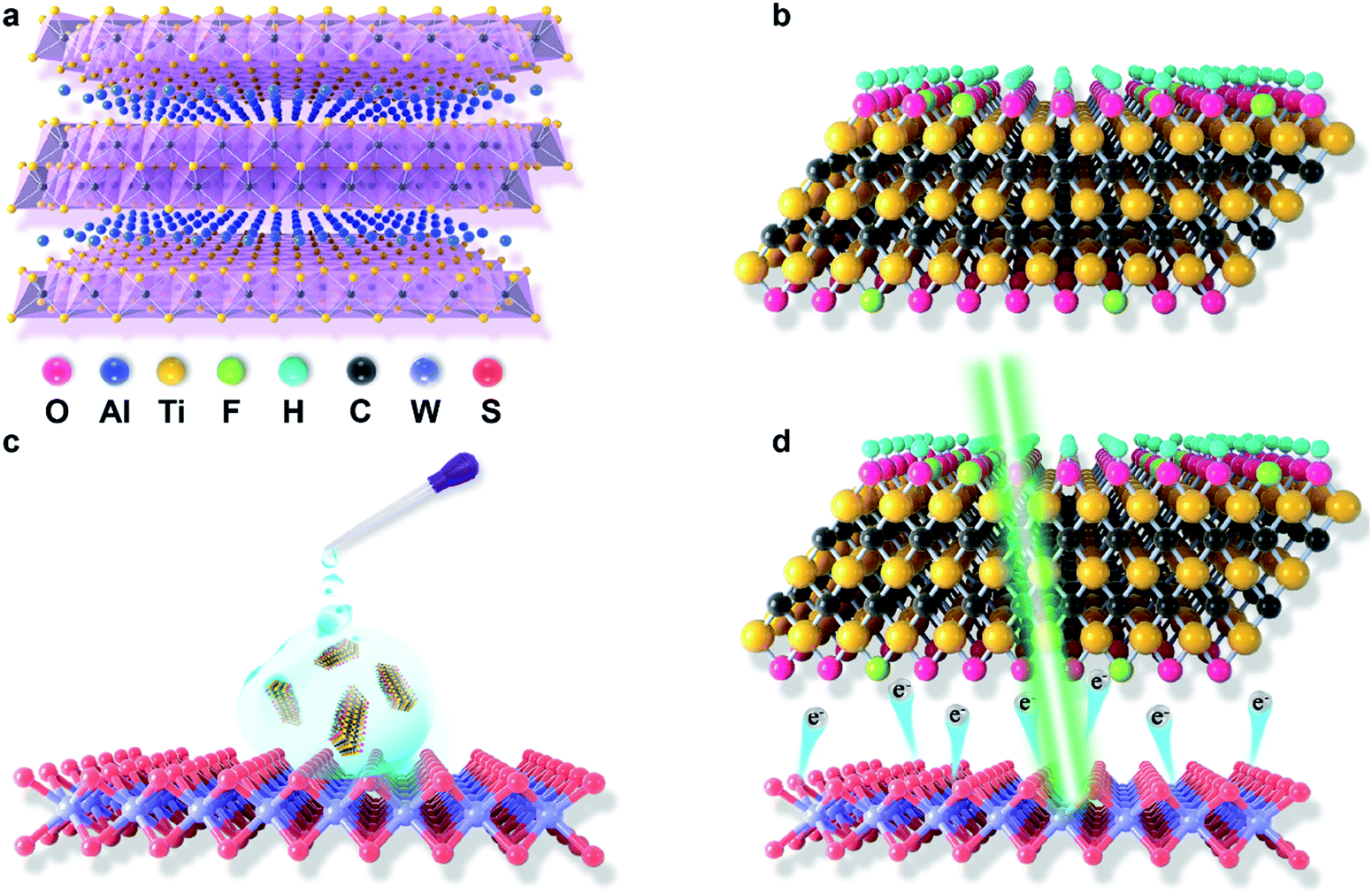
Recently, a new type of 2D transition metal carbide (MXene) has been produced and synthesized from the MAX phase.27 The MAX phases are commonly represented by the chemical formula of Mn+1AXn (Fig. 1a), where A represents the main group element, X is C and/or N, M is an early transition metal, and n = 1, 2 or 3.28 Owing to the wet etching of the MAX phase in a fluoride-containing solution to remove A element and then delaminate the layers, the surface of the resulting MXene is always terminated by a mixture of functional groups of –F, –O and/or –OH with the corresponding chemical formula of Mn+1XnTx (Fig. 1b), where T represents the terminated functional group, and x is the atomic percentage of terminated functional group.29 MXenes have attracted exponential attention in diverse fields including supercapacitance,30 electromagnetic interference (EMI) shielding,31 nonlinear photonics,32,33 Li-ion and other types of battery fabrication,34 photo-detection,35 energy storage,36 photothermal therapy37 as well as water purification38 because of their unique chemical and physical properties. In addition, the superior hydrophilicity of MXenes allows it to be easily dispersed in solution, making it a promising candidate for solution processing. Notably, according to the recent theoretical studies, MXenes were theoretically indicated for controlling the electronic density of TMDCs via tuning the surface functional group; nevertheless, this idea has not yet been experimentally explored.39 In this study, as a proof of concept, we deposited the MXene solution onto 1-layer (1L) tungsten disulfide (WS2) via the drop-casting method to tune exciton/trion-involved optoelectronic properties of 1L WS2 (Fig. 1c and d). MXene-decorated WS2 successfully achieved a ∼5-fold PL enhancement than the pristine WS2, which could have originated from the effective charge transfer from WS2 to MXenes induced by a strong electron-withdrawing effect of the attached surface functional group. We also reveal that this electron-withdrawing ability of MXenes can be well modulated by tuning its corresponding surface functional group via a post-etch annealing method. This study not only extends the application area of MXenes, but also develops a simple and green strategy to achieve bright photoluminescence with high quantum yields in monolayer WS2.
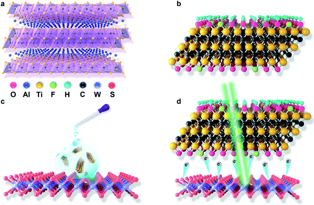 |
| | Fig. 1 Schematic of the MAX phase of Ti3AlC2 (a), HF-etched and delaminated MXene (F–Ti3C2Tx) nano-flakes (b), F–Ti3C2Tx nano-flakes doping in 1 L WS2via drop-coating (c) and (d) withdrawal of electrons from monolayer WS2 to F–Ti3C2Tx nano-flakes under the 532 nm laser excitation. | |
2. Experimental section
2.1. Synthesis of Ti3C2Tx MXenes
MAX phase Ti3AlC2 with a purity of 98% was purchased from Beijing Forsman Pte Ltd. F–Ti3C2Tx MXenes were made by etching MAX-phased Ti3AlC2 in 48% HF at 60 °C for over 24 h. After etching, the samples were washed and centrifuged (3500 rpm) for 20 min with DI water for 5 times to obtain pH ≥ 5 in an aqueous phase. The resulting solution was vacuum-filtered using a micropore PTFE 0.2 μm filter to obtain the MXene powder. The delamination of MXene flakes was performed by hand-shaking of the sample for 5 min, followed by centrifugation at 3500 rpm for 1 h.35 The resulting concentrated aqueous colloidal solution of Ti3C2Tx MXene sheets was used for the doping of 1 L WS2. Due to the etching process, Ti3C2 MXene contains fluorine elements; hence, the resulting materials will be referred to as F–Ti3C2Tx in this study. N-doped Ti3C2Tx was prepared using the post-annealing method. F–Ti3C2Tx was placed in a tube CVD in a NH3/Ar atmosphere at 400 °C for 4.5 h to obtain N–Ti3C2Tx.
2.2. Characterization
The Raman spectra, PL spectra and mapping were conducted using a WITec alpha 300 R system at excitation wavelengths of 488 and 532 nm, respectively. In order to avoid heating and optical doping effect, the power of the laser was kept as low as 10 μW for the room temperature PL measurement. The AFM measurement was performed using a cyphers. The crystal structure, sample size, morphologies, and surface element were determined via X-ray diffraction (XRD), transmission electron microscopy (TEM) and X-ray photoelectron spectroscopy (XPS).
2.3. Mxene doping
MXenes were dispersed in an isopropanol (IPA) solution at a concentration of ∼10 mg mL−1. The dopant of MXenes was deposited via a drop-casting method. The volume of doping was ∼10 μL. All the measurements were performed after the sample was dried under an ambient condition.
3. Result and discussion
3.1. MXene nano-flake preparation and characterization
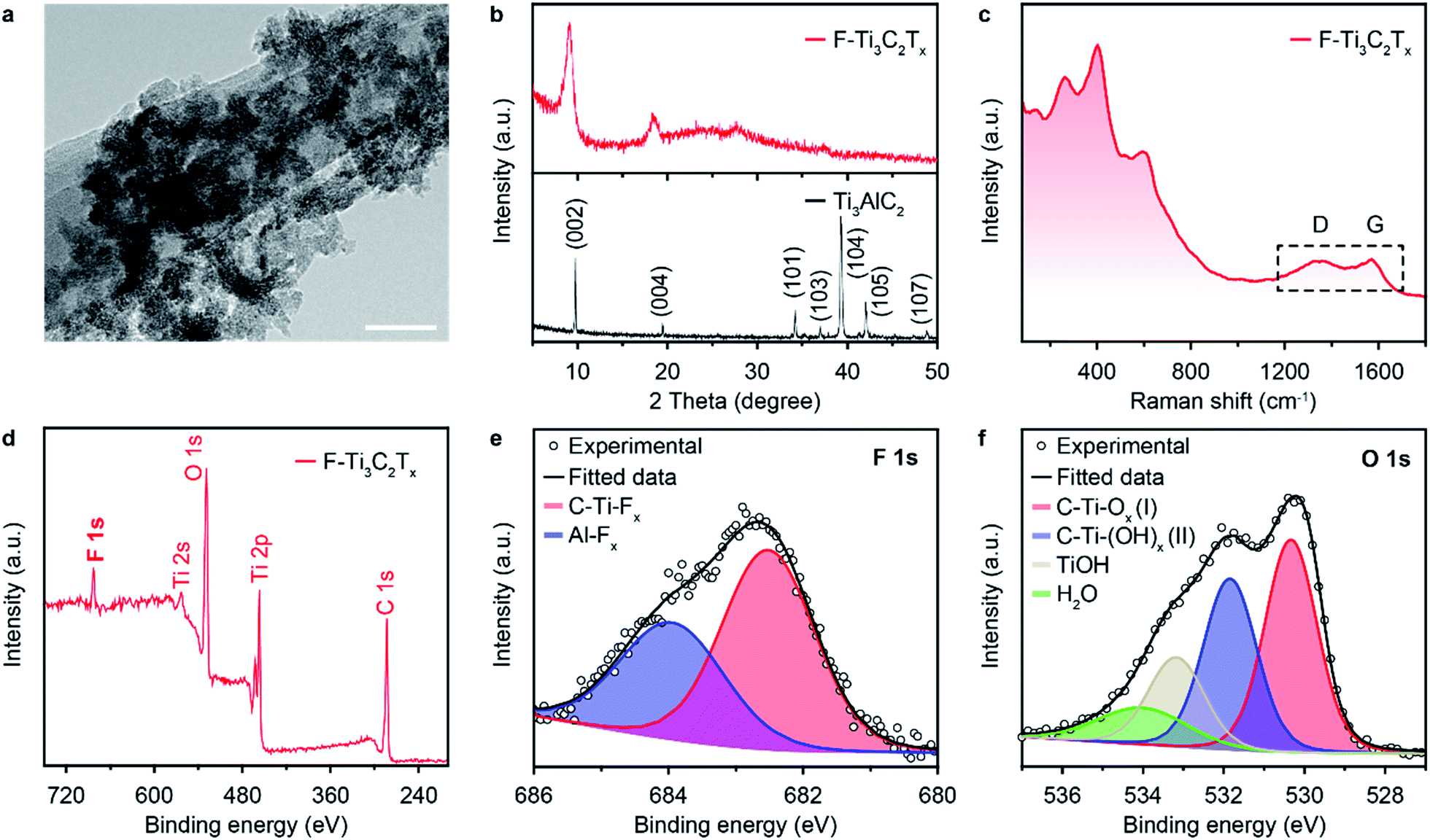
The MXene (F–Ti3C2Tx) nano-flakes can be conventionally prepared via a sequence of etching and delamination processes (see Experimental section). The typical morphology of MXene nano-flakes was characterized via transmission electron microscopy (TEM). As shown in Fig. 2a, the thin F–Ti3C2Tx nano-flakes are dispersed as a stack of few layers. To further characterize the quality of the exfoliated F–Ti3C2Tx nano-flakes, X-ray diffraction (XRD) and Raman spectroscopy were also performed. The XRD pattern (Fig. 2b, bottom, black line) of Ti3AlC2 MAX phase shows the typical (002), (004), (101), (103), (104), (105), and (107) XRD peaks at 2θ degree of 9.78°, 19.47°, 34.10°, 36.95°, 39.30°, 42.07°, and 48.88°, respectively, which is in accordance with previous reports.40 The disappearance of a strong (104) peak at 2θ = 39.30° demonstrates the successful preparation of F–Ti3C2Tx nano-flakes through the removal of Al atom (Fig. 2b, top, red line). Furthermore, the as-prepared F–Ti3C2Tx nano-flakes showed a lower 2θ degree (9.14°) and a broader peak compared to that of Ti3AlC2, which suggests a change in the c-lattice parameter and decreased the structure order in F–Ti3C2Tx nano-flakes, reconfirming the successful delamination.41 The Raman spectrum shown in Fig. 2c exhibits several vibration modes with peaks at 262.91, 403.46, 520.41 and 597.47 cm−1, which could be assigned to nonstoichiometric titanium carbides.42 Additional peaks at 1347.58 and 1573.93 cm−1 could have originated from the D and G bands of carbon layers in the as-prepared F–Ti3C2Tx nano-flakes.42 X-ray photoelectron spectroscopy (XPS) investigations were conducted to characterize the surface chemical compositions of the as-prepared F–Ti3C2Tx nano-flakes. The full-spectrum XPS (Fig. 2d) reveals several elements including titanium, carbon, oxygen and fluoride, demonstrating the presence of –O, –F and –OH terminations on the surface of F–Ti3C2Tx nano-flakes.41,43 The high-resolution XPS spectra of F–Ti3C2Tx nano-flakes in F regions can be fitted using two peaks centred at 683.99 and 682.5 eV, indicating the existence of both Ti–F and Al–F, respectively. The O 1s core level can be deconvoluted into four components at 533.80, 532.91, 531.84 and 530.73 eV, which can be attributed to H2O, Ti–OH, C–Ti(OH)x and C–Ti–Ox, respectively. The XPS spectrum of Ti 2p (Fig. S1†) verifies the presence of Ti–C, Ti–O and Ti–F, respectively. Moreover, the high-resolution C 1s XPS spectrum shows three fitting peaks, corresponding to C–Ti, C–C, and C–O, respectively (Fig. S2†).
 |
| | Fig. 2 (a) TEM images, (b) XRD patterns and (c) Raman spectrum of F–Ti3C2Tx nano-flakes. (d–f) XPS spectra of F–Ti3C2Tx nano-flakes in (d) full spectrum region, (e) F 1s region and (f) O 1s region. Shaded colored areas in (e) and (f) represent curve-fitting results. The scale bar in (a) is 50 nm. | |
3.2. Preparation and characterization of tungsten disulfide
To demonstrate the exciton modulation of 1L WS2via MXene deposition, we prepared a monolayer WS2. The standard micromechanical method was used to exfoliate 1L-WS2 from bulk crystals via a Scotch tape and transferred onto a silicon (Si) wafer with a 280 nm thick thermal oxidation (SiO2) coated layer.44 The exfoliated WS2 flakes were determined by an optical microscope image, Raman spectrum, atomic force microscopy (AFM) and PL measurement to determine their exact layer number. The typical optical microscope image of 1L-WS2 flakes on SiO2/Si is shown in Fig. S3a.† The thickness of exfoliated flakes is revealed by the AFM height profile based on a non-contact mode, and measured along the white dot line crossing the flakes. The thickness of the 1-layer WS2 is about 0.8 nm, as shown in Fig. S3b and c,† in which the slight drop in the boundaries may be induced by the absorbed residues and/or molecules. The Raman spectrum (Fig. S4†) of exfoliated flake excited with a 488 nm laser exhibits two strong peaks at about 355 and 417 cm−1, which can be defined as in-plane E12g and out-of-plane A1g vibration modes, respectively. The difference (Δ) between A1g and E12g peaks is ∼62.3 cm−1, (Δ = A1g − E12g), confirming the monolayer feature of the exfoliated WS2 flake.45 In addition, the PL mapping measurement was adapted to verify the monolayer characteristics of the exfoliated flakes. The bright emission of the monolayer WS2 (Fig. S5a†) is observed in the dot area in Fig. S3a.† However, on the account of the transition from direct band gap monolayer to indirect band gap multi-layer, the PL intensity of other area in Fig. S3a† cannot be observed.17 It should be noted that the intensities of the PL mapping are slightly uneven, which may be caused by the non-uniformity natural n-doping effect in exfoliated 1L WS2. The weaker PL emission area should have a higher n-doping level compared to the higher PL intensity area, which would lead to the increased emission from low-intensity negative trions formed via the combination of excess electrons and neutral excitons (Fig. S5b†) in the extracted PL spectrum.46 Moreover, the spectrum exhibits a peak at around 1.97 eV for monolayer WS2 (Fig. S5b†), which is similar to that reported previously. As the strong spin–orbit interaction induced energy difference of A and B excitons in the emission spectrum is as large as ∼0.4 eV, the emission from B exciton was not detected under a 532 nm laser excitation.47
3.3. Exciton/trion modulation via MXene doping
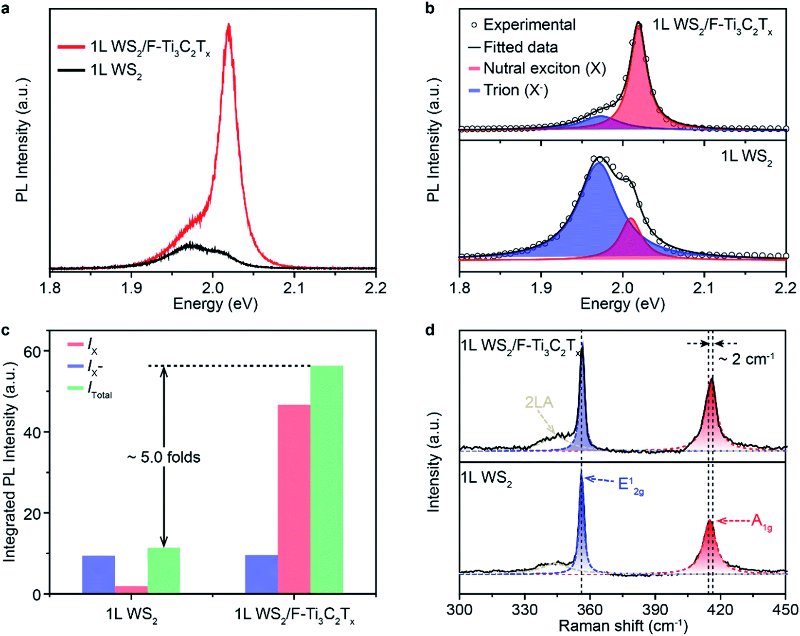
To test the superiority of F–Ti3C2Tx nano-flakes in controlling the carrier density of WS2, F–Ti3C2Tx nano-flakes were deposited onto 1L WS2 by drop-casting. A direct evidence to indicate the successful electron modulation in WS2 is the enhanced PL emission. Pristine WS2 shows a weak PL emission with a peak centred at ∼1.97 eV (Fig. 3a). The low emission intensity and relatively small peak energy could have originated from the heavy n-doping feature in pristine 1L WS2.46 After the coupling of F–Ti3C2Tx and 1L WS2, the PL intensity of 1L WS2/F–Ti3C2Tx has remarkably increased, which is almost ∼5.0 folds more than that of pristine 1L WS2 (Fig. 3c). Meanwhile, the peak position is also blue shifted to ∼2.02 eV. To clearly figure out the variation in PL properties caused by F–Ti3C2Tx nano-flake doping, the Lorentzian fitting was performed. The fitted results of 1L WS2/F–Ti3C2Tx and 1L WS2 are shown in the top and bottom panels of Fig. 3b, respectively. The peaks of 1L WS2/F–Ti3C2Tx and 1L WS2 can be well fitted by assuming two peaks of neutral exciton (X) and negative trion (X−) peaks.25 According to the fitted results, the dominant peak is assigned to the negative trion with a spectral weight (IX−/Itotal) of up to ∼0.82 (Fig. 3b and c). It should be noted that the neutral exciton peak becomes predominant and the weight of the negative trion of 1L WS2/F–Ti3C2Tx is greatly decreased to ∼0.18. The variation in the PL intensity and peak position could be ascribed to the transition from negative trions to neutral excitons after F–Ti3C2Tx nano-flake doping. The exciton transition could be well explained by the p-type doping, which can significantly decrease the electron density of 1L WS2.24 According to the previous report, the A1g vibration mode of 1L WS2 Raman spectrum is very susceptible to electron coupling. The decrease in the electron density could cause blue-shifting of the A1g vibration mode.17 Therefore, in order to confirm the change in the electron density in 1L WS2/F–Ti3C2Tx, the Raman spectra of 1L WS2/F–Ti3C2Tx was measured. As shown in Fig. 3d, the Raman spectrum of 1L WS2/F–Ti3C2Tx shows a blue-shifted A1g vibration mode of ∼2 cm−1, indicating the decrease in the electron density of 1L WS2/F–Ti3C2Tx. Consequently, the variation in PL and Raman properties could originate from the withdrawal of electrons from 1L WS2 to F–Ti3C2Tx nano-flakes owing to the surface electron-withdrawing group and physically and/or chemically adsorbed H2O of F–Ti3C2Tx nano-flakes (Fig. 1b and d).17,45
 |
| | Fig. 3 (a) PL spectra of 1L WS2 and 1L WS2/F–Ti3C2Tx measured at room temperature. The doping of F–Ti3C2Tx nano-flakes clearly modified the PL intensity and peak positions. (b) Fitted PL spectra of 1L WS2 and 1L WS2/F–Ti3C2Tx. Note that the peaks in PL spectra were fitted using the Lorentzian fitting by assuming two peaks of the neutral exciton (X) and trion (X−) peaks. (c) The integrated PL intensity of the neutral excitons (IX), trions (IX−), and the sum (Itotal) of IX and IX− of 1L WS2 and 1L WS2/F–Ti3C2Tx, respectively. (d) Raman spectra of 1L WS2 and 1L WS2/F–Ti3C2Tx. A slightly blue shift by ∼2.0 cm−1 was observed in the A1g mode of 1L WS2/F–Ti3C2Tx compared to that of pristine 1L WS2. | |
3.4. Effect of surface functional group of MXenes on PL enhancement
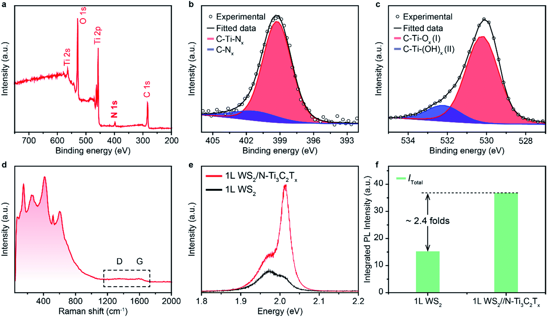
In order to figure out the vital role of the surface electron-withdrawing group and adsorbed H2O of MXene nano-flakes on the enhancement of the PL emission of 1L WS2, a control experiment was performed using an as-synthesized nitrogen (N)-substituted MXene (N–Ti3C2Tx) as a dopant. N–Ti3C2Tx was constructed by annealing HF-etched Ti3C2Tx in ammonia at 700 °C and characterized by XPS and Raman spectra.40 The full-spectrum XPS reveals several elements, including titanium, carbon, oxygen and nitrogen, demonstrating the presence of –O, –OH and –N terminations on the surface of N–Ti3C2Tx nano-flakes (Fig. 4a). It should be noted that the strong electron-withdrawing F functional group was successfully eliminated at high temperatures, which would significantly decrease the electron-withdrawing ability of N–Ti3C2Tx nano-flakes.48 The high-resolution XPS spectra of the N–Ti3C2Tx nano-flakes in N regions can be fitted using two peaks centred at 401.45 and 399.25 eV (Fig. 4b), indicating the existence of both C–N and Ti–N, respectively. The O 1s core level can be deconvoluted into two components at 532.21 and 530.73 eV, which could be attributed to C–Ti(OH)x, and C–Ti–Ox, respectively (Fig. 4c). This demonstrates the removal of physically and/or chemically adsorbed H2O at high temperatures, suggesting a further decrease in the electron-withdrawing ability of N–Ti3C2Tx nano-flakes. The Raman spectrum of N–Ti3C2Tx nano-flakes is similar to that of F–Ti3C2Tx nano-flakes owing to the preserved Ti3C2 structure (Fig. 4d). It is worth noting that the D and G bands almost disappear, indicating the disordered carbon sheets of N–Ti3C2Tx nano-flakes induced by the N-intercalation. To verify the evolution of the PL emission of 1L WS2via N–Ti3C2Tx nano-flake doping, the PL spectrum of 1L WS2/N–Ti3C2Tx was measured. As shown in Fig. 4e, although 1L WS2/N–Ti3C2Tx also shows an improved PL emission with an exciton transition from negative trion to neutral exciton, the PL enhancement is much lower (∼2.41 folds) compared to that of 1L WS2/F–Ti3C2Tx (Fig. 4f). The decreased PL enhancement of 1L WS2/N–Ti3C2Tx could be attributed to the decreased charge transfer from 1L WS2 to N–Ti3C2Tx owing to the elimination of a strong electron-withdrawing functional group of F and adsorbed H2O.17,45
 |
| | Fig. 4 (a–c) X-ray photoelectron (XPS) spectra of F–Ti3C2Tx nano-flakes in (a) full-spectrum region, (b) N 1s region and (c) O 1s region. Shaded colored areas in (b) and (c) represent curve-fitting results. (d) Raman spectrum of N–Ti3C2Tx nano-flakes. (e) PL spectra of 1L WS2 and 1L WS2/N–Ti3C2Tx measured at room temperature. (f) The integrated total (Itotal) PL intensity of 1L WS2 and 1L WS2/F–Ti3C2Tx. | |
4. Conclusions
In summary, we succeeded in achieving the p-type doping of 1L-WS2via surface functional group-modified MXene nano-flakes. Upon doping with MXene nano-flakes, the blue-shifted A1g vibration mode and enhanced PL efficiency of neutral excitons can be obviously observed. These findings can serve as a direct proof of the regulated optoelectronic properties of 1L WS2, demonstrating that the p-doping effect is dominant in surface functional group-modified MXene nano-flake-doped 1L-WS2. The modulation of the optoelectronic properties of 1L WS2 by drop-coating with MXene nano-flakes could be ascribed to the effective charge transfer from 1L WS2 to MXenes induced by strong electron-withdrawing characteristics inherited from the surface fluorine functional group and/or adsorbed H2O presented on the MXene nano-flakes. In addition, the electron-withdrawing ability of MXenes can be facilely controlled by tuning the type of surface functional groups. These findings suggest that 2D MXenes are promising materials for regulating the optical and electronic properties of 1L-WS2, offering a new avenue to construct new heterostructure junctions, such as high-performance photodetectors, ambipolar transport field effect transistors, and flexible solar energy harvesting devices, and broadening the horizon for harnessing the unique properties of MXenes.
Conflicts of interest
There are no conflicts to declare.
Acknowledgements
This work is supported by SERC (Grant No. 1426500050) from the Agency for Science, Technology and Research (A*STAR), Singapore National Research Foundation, Competitive Research Program (Grant No. NRF-CRP18-2017-02), Singapore Ministry of Education Tier 2 Program (Grant No. MOE2016-T2-1-128) and National Natural Science Foundation of China (Grant No. 61704082) and Natural Science Foundation of Jiangsu Province (Grant No. BK20170851). H. Li would like to thank the support from Nanyang Technological University under NAP award (M408050000) and Singapore Ministry of Education Tier 1 program (2018-T1-001-051).
Notes and references
- M. Amani, D. H. Lien, D. Kiriya, J. Xiao, A. Azcatl, J. Noh, S. R. Madhvapathy, R. Addou, S. KC, M. Dubey, K. Cho, R. M. Wallace, S. C. Lee, J. H. He, J. W. Ager, X. Zhang, E. Yablonovitch and A. Javey, Science, 2015, 350, 1065–1068 CrossRef CAS.
- W. Choi, N. Choudhary, G. H. Han, J. Park, D. Akinwande and Y. H. Lee, Mater. Today, 2017, 20, 116–130 CrossRef CAS.
- S. Manzeli, D. Ovchinnikov, D. Pasquier, O. V. Yazyev and A. Kis, Nat. Rev. Mater., 2017, 2, 17033 CrossRef CAS.
- X. Yu, P. Yu, D. Wu, B. Singh, Q. Zeng, H. Lin, W. Zhou, J. Lin, K. Suenaga, Z. Liu and Q. J. Wang, Nat. Commun., 2018, 9, 1545 CrossRef PubMed.
- X. Duan, C. Wang, A. Pan, R. Yu and X. Duan, Chem. Soc. Rev., 2015, 44, 8859–8876 RSC.
- C. L. Tan and H. Zhang, Chem. Soc. Rev., 2015, 44, 2713–2731 RSC.
- J. Pu and T. Takenobu, Adv. Mater., 2018, 30, 1707627 CrossRef PubMed.
- S. C. Dhanabalan, J. S. Ponraj, Z. Guo, S. Li, Q. Bao and H. Zhang, Adv. Sci., 2017, 4, 1600305 CrossRef PubMed.
- S. Wang, A. Robertson and J. H. Warner, Chem. Soc. Rev., 2018, 47, 6764–6794 RSC.
- J. S. Ross, S. Wu, H. Yu, N. J. Ghimire, A. M. Jones, G. Aivazian, J. Yan, D. G. Mandrus, D. Xiao, W. Yao and X. Xu, Nat. Commun., 2013, 4, 1474 CrossRef PubMed.
- Y. Zhang, C. Lim, Z. Dai, G. Yu, J. W. Haus, H. Zhang and P. N. Prasad, Phys. Rep., 2019, 795, 1–51 CrossRef CAS.
- L. J. Li, E. C. O'Farrell, K. P. Loh, G. Eda, B. Ozyilmaz and N. A. Castro, Nature, 2016, 529, 185–189 CrossRef CAS PubMed.
- J. Pei, J. Yang, X. Wang, F. Wang, S. Mokkapati, T. Lü, J. Zheng, Q. Qin, D. Neshev, H. H. Tan, C. Jagadish and Y. Lu, ACS Nano, 2017, 11, 7468–7475 CrossRef CAS PubMed.
- J. D. Lin, C. Han, F. Wang, R. Wang, D. Xiang, S. Qin, X. Zhang, L. Wang, H. Zhang, A. T. S. Wee and W. Chen, ACS Nano, 2014, 8, 5323–5329 CrossRef CAS PubMed.
- J. Pei, J. Yang, T. Yildirim, H. Zhang and Y. Lu, Adv. Mater., 2019, 31, 1706945 CrossRef PubMed.
- Z. Hu, Z. Wu, C. Han, J. He, Z. Ni and W. Chen, Chem. Soc. Rev., 2018, 47, 3100–3128 RSC.
- N. Peimyoo, W. Yang, J. Shang, X. Shen, Y. Wang and T. Yu, ACS Nano, 2014, 8, 11320–11329 CrossRef CAS PubMed.
- X. Chen and A. R. McDonald, Adv. Mater., 2016, 28, 5738–5746 CrossRef CAS PubMed.
- S. Zhang, H. M. Hill, K. Moudgil, C. A. Richter, A. R. Hight Walker, S. Barlow, S. R. Marder, C. A. Hacker and S. J. Pookpanratana, Adv. Mater., 2018, 30, 1802991 CrossRef PubMed.
- C. Cong, J. Shang, Y. Wang and T. Yu, Adv. Opt. Mater., 2016, 6, 1700767 CrossRef.
- Z. Wang, Z. Dong, Y. Gu, Y. Chang, L. Zhang, L. Li, W. Zhao, G. Eda, W. Zhang, G. Grinblat, S. A. Maier, J. K. W. Yang, C. Qiu and A. T. S. Wee, Nat. Commun., 2016, 7, 11283 CrossRef CAS PubMed.
- Y. I. Jhon, Y. Kim, J. Park, J. H. Kim, T. Lee, M. Seo and Y. M. Jhon, Adv. Funct. Mater., 2016, 26, 7551–7559 CrossRef CAS.
- Y. Sun, Z. Zhou, Z. Huang, J. Wu, L. Zhou, Y. Cheng, J. Liu, C. Zhu, M. Yu, P. Yu, W. Zhu, Y. Liu, J. Zhou, B. Liu, H. Xie, Y. Cao, H. Li, X. Wang, K. Liu, X. Wang, J. Wang, L. Wang and W. Huang, Adv. Mater., 2019, 31, 1806562 CrossRef PubMed.
- C. R. Ryder, J. D. Wood, S. A. Wells and M. C. Hersam, ACS Nano, 2016, 10, 3900–3917 CrossRef CAS PubMed.
- S. Mouri, Y. Miyauchi and K. Matsuda, Nano Lett., 2013, 13, 5944–5948 CrossRef CAS PubMed.
- Y. Tao, X. Yu, J. Li, H. Liang, Y. Zhang, W. Huang and Q. J. Wang, Nanoscale, 2018, 10, 6294–6299 RSC.
- M. Ghidiu, M. R. Lukatskaya, M. Zhao, Y. Gogotsi and M. W. Barsoum, Nature, 2014, 516, 78–171 CrossRef CAS PubMed.
- M. Naguib, V. N. Mochalin, M. W. Barsoum and Y. Gogotsi, Adv. Mater., 2014, 26, 992–1005 CrossRef CAS PubMed.
- H. Lin, Y. Chen and J. Shi, Adv. Sci., 2018, 5, 1800518 CrossRef PubMed.
- M. Hu, T. Hu, Z. Li, Y. Yang, R. Cheng, J. Yang, C. Cui and X. Wang, ACS Nano, 2018, 12, 3578–3586 CrossRef CAS PubMed.
- J. Liu, H. Zhang, R. Sun, Y. Liu, Z. Liu, A. Zhou and Z. Yu, Adv. Mater., 2017, 29, 1702367 CrossRef PubMed.
- X. Jiang, S. Liu, W. Liang, S. Luo, Z. He, Y. Ge, H. Wang, R. Cao, F. Zhang, Q. Wen, J. Li, Q. Bao, D. Fan and H. Zhang, Laser Photonics Rev., 2018, 12, 1700229 CrossRef.
- L. Wu, X. Jiang, J. Zhao, W. Liang, Z. Li, W. Huang, Z. Lin, Y. Wang, F. Zhang, S. Lu, Y. Xiang, S. Xu, J. Li and H. Zhang, Laser Photonics Rev., 2018, 12, 1800215 CrossRef.
- M. Naguib, J. Come, B. Dyatkin, V. Presser, P. Taberna, P. Simon, M. W. Barsoum and Y. Gogotsi, Electrochem. Commun., 2012, 16, 61–64 CrossRef CAS.
- S. Chertopalov and V. N. Mochalin, ACS Nano, 2018, 12, 6109–6116 CrossRef CAS PubMed.
- B. Anasori, M. R. Lukatskaya and Y. Gogotsi, Nat. Rev. Mater., 2017, 2, 16098 CrossRef CAS.
- C. Xing, S. Chen, X. Liang, Q. Liu, M. Qu, Q. Zou, J. Li, H. Tan, L. Liu, D. Fan and H. Zhang, ACS Appl. Mater. Interfaces, 2018, 10, 27631–27643 CrossRef CAS PubMed.
- L. Ding, Y. Wei, Y. Wang, H. Chen, J. Caro and H. Wang, Angew. Chem., Int. Ed., 2017, 56, 1825–1829 CrossRef CAS PubMed.
- Y. Liu, H. Xiao and W. A. Goddard, J. Am. Chem. Soc., 2016, 138, 15853–15856 CrossRef CAS PubMed.
- Y. Wen, T. E. Rufford, X. Chen, N. Li, M. Lyu, L. Dai and L. Wang, Nano Energy, 2017, 38, 368–376 CrossRef CAS.
- S. Tu, Q. Jiang, X. Zhang and H. N. Alshareef, ACS Nano, 2018, 12, 3369–3377 CrossRef CAS PubMed.
- K. Krishnamoorthy, P. Pazhamalai, S. Sahoo and S. Kim, J. Mater. Chem. A, 2017, 5, 5726–5736 RSC.
- S. J. Kim, H. Koh, C. E. Ren, O. Kwon, K. Maleski, S. Cho, B. Anasori, C. Kim, Y. Choi, J. Kim, Y. Gogotsi and H. Jung, ACS Nano, 2018, 12, 986–993 CrossRef CAS PubMed.
- X. Yu, S. Zhang, H. Zeng and Q. J. Wang, Nano Energy, 2016, 25, 34–41 CrossRef CAS.
- H. M. Oh, H. Jeong, G. H. Han, H. Kim, J. H. Kim, S. Y. Lee, S. Y. Jeong, S. Jeong, D. J. Park, K. K. Kim, Y. H. Lee and M. S. Jeong, ACS Nano, 2016, 10, 10446–10453 CrossRef CAS PubMed.
- P. K. Chow, R. B. Jacobs-Gedrim, J. Gao, T. Lu, B. Yu, H. Terrones and N. Koratkar, ACS Nano, 2015, 9, 1520–1527 CrossRef CAS PubMed.
- B. Zhu, H. Zeng, J. Dai and X. Cui, Adv. Mater., 2014, 26, 5504–5507 CrossRef CAS PubMed.
- S. Lai, J. Jeon, S. K. Jang, J. Xu, Y. J. Choi, J. Park, E. Hwang and S. Lee, Nanoscale, 2015, 7, 19390–19396 RSC.
Footnotes |
| † Electronic supplementary information (ESI) available. See DOI: 10.1039/c9na00395a |
| ‡ These authors contributed equally to this work. |
|
| This journal is © The Royal Society of Chemistry 2019 |
Click here to see how this site uses Cookies. View our privacy policy here. 
 Open Access Article
 This Open Access Article is licensed under a Creative Commons Attribution-Non Commercial 3.0 Unported Licence
 a,
Chongwu
Wang
a,
Houkun
Liang
c,
Ying
Zhang
c,
Hong
Li
a,
Chongwu
Wang
a,
Houkun
Liang
c,
Ying
Zhang
c,
Hong
Li