
 Open Access Article
 This Open Access Article is licensed under a Creative Commons Attribution-Non Commercial 3.0 Unported Licence
A low Schottky barrier height and transport mechanism in gold–graphene–silicon (001) heterojunctions†
Jules
Courtin
ab,
Sylvain
Le Gall
c,
Pascal
Chrétien
c,
Alain
Moréac
ab,
Gabriel
Delhaye
ab,
Bruno
Lépine
ab,
Sylvain
Tricot
ab,
Pascal
Turban
ab,
Philippe
Schieffer
ab and
Jean-Christophe
Le Breton
 *ab
*ab
aUniv. Rennes, CNRS, IPR (Institut de Physique de Rennes), UMR 6251, F-35000 Rennes, France. E-mail: jean-christophe.lebreton@univ-rennes.fr
bDépartement Matériaux et Nanosciences, Institut de Physique de Rennes, UMR 6251, CNRS, Université de Rennes 1, Campus de Beaulieu, Bât 11E, 35042 Rennes cedex, France
cGroup of Electrical Engineering Paris (GeePs), CNRS, CentraleSupélec, Univ. Paris-Sud, Sorbonne Université, CEDEX, 11 rue Joliot-Curie, 91192 Gif-sur-Yvette, France
First published on 27th July 2019
Abstract
The interface resistance at metal/semiconductor junctions has been a key issue for decades. The control of this resistance is dependent on the possibility to tune the Schottky barrier height. However, Fermi level pinning in these systems forbids a total control over interface resistance. The introduction of 2D crystals between semiconductor surfaces and metals may be an interesting route towards this goal. In this work, we study the influence of the introduction of a graphene monolayer between a metal and silicon on the Schottky barrier height. We used X-ray photoemission spectroscopy to rule out the presence of oxides at the interface, the absence of pinning of the Fermi level and the strong reduction of the Schottky barrier height. We then performed a multiscale transport analysis to determine the transport mechanism. The consistency in the measured barrier height at different scales confirms the good quality of our junctions and the role of graphene in the drastic reduction of the barrier height.
Introduction
Metal/Si (M/Si) junctions are one of the most important interfaces for Si-based devices. Drastic reduction of the contact resistivity at M/Si interfaces is necessary for next generation CMOS technology. The contact resistivity is directly determined by the height and width of the Schottky barrier formed at the M/Si interface. For n-type silicon, the reduction of interface resistance can be achieved by the reduction of the barrier width i.e. by the reduction of the space charge region width via heavy doping. However, as devices are scaled down, leakage current and dopant profile control becomes increasingly difficult. Moreover, doping techniques such as implantation and diffusion require high temperatures in the 1000 °C range which may be incompatible with some processes like MEMS integration. Au–Sb alloys may form ohmic contacts with Si at a lower temperature of around 360 °C.For the Schottky barrier height (SBH), reduction is more difficult because of the pinning of the Fermi level (FL) at approximately midgap in Si.1 Attempts to alleviate FL pinning in semiconductors have been made in the past by the introduction of a thin insulating barrier2,3 or surface passivation.4 A new and promising route towards this goal is the introduction of a 2D crystal between M and Si. As they are ultimately thin, 2D crystals would reduce the resistance increase due to insulator barriers and tune the work function.5,6 Graphene (G), a one-atom-thick layer of carbon in a honeycomb crystal lattice, avoids the formation of undesired interface states and/or metal induced states at the Si surface.7,8 Moreover, the work function of graphene can be modulated by doping with various metals.9,10 Several experimental results show that, unlike other metals, the Fermi level pinning can be alleviated with graphene on Si.11,12 The literature on M/G/Si shows a variety of results. When heavily doped Si is used, the G layer acts as an almost transparent tunnel barrier which makes it a promising candidate for spin filtering for example.13–15 For lower doped Si, a reduced interface resistance or SBH has been observed for M/G/Si compared to M/Si.5,11,16 On the other hand, other groups report no influence of the G layer at all but with a large variation between the measured SBHs7,17 for similar stacks. Similar to what can be found for G/Si Schottky contacts, a number of different characterisation techniques, transport models and sample preparation methods make the comparison between different results difficult. For that reason, we present here a multiscale analysis of a Au/G/Si:H junction studied with different techniques in order to give a consistent description of the band alignments and determine the transport mechanism.
We used X-ray photoemission spectroscopy (XPS) to study the formation of Au/G/Si contacts. Core level peak positions were used to determine the energy band alignment. Capacitance–voltage (C–V) and current–voltage (J–V) measurements and conductive-probe atomic force microscopy (CP-AFM) were then used to determine the apparent electronic SBH, transport mechanism and contact homogeneity. Using these multiscale techniques, we demonstrate the absence of FL pinning and strong reduction of the SBH induced by the insertion of monolayer graphene between Au and hydrogen-passivated silicon (Si:H).
Experimental details
Single layer graphene realized by chemical vapor deposition on copper was purchased from Graphenea©. A 200 nm polymethyl methacrylate (PMMA) layer was then deposited on top. After PMMA coating, copper was etched in a FeCl3 solution until no metallic copper could be seen and the floating PMMA/graphene was rinsed several times in deionized water. Graphene was then transferred onto a Si substrate with a resistivity of 1–10 Ω cm. Si was degreased in acetone and isopropyl alcohol followed by 30 minutes of UV/ozone cleaning leading to the formation of a thin SiO2 layer of about 1 nm (see the ESI†). The floating PMMA/graphene was deposited onto the oxidized silicon and left to dry for 30 minutes at 50 °C followed by 15 minutes at 135 °C. After removal of PMMA in acetone, the samples were introduced into an Ultra High Vacuum (UHV) chamber where they were annealed at 300 °C for 3 hours to remove resist residues. The samples were then taken out of the UHV chamber for a final oxide etch in 2% hydrofluoric acid (HF) before re-introduction into the UHV chamber. Au was then sequentially deposited at room temperature by molecular beam epitaxy with an effusion cell at a rate of 0.2–0.4 Å min−1 for submonolayer thicknesses and 1–2 Å min−1 otherwise. The Si 2p and C 1s core levels were monitored as a function of gold thickness. Metal deposition and photoemission measurements were performed in a multichamber UHV system with base pressures below 2 × 10⁻¹⁰ mbar. XPS measurements at normal emission were performed at room temperature using a Mg Kα (1253.6 eV) source. The kinetic energy of the emitted electrons has been measured by employing a hemispherical analyzer (Omicron EA125) with a five channel detection system. The total energy resolution was 0.80 eV. The Au 4f7/2 peak position from a thick gold sample, assumed to be 84.00 eV BE,18 was taken as a reference in order to position the Fermi level (FL). For the determination of the SBHs and Si band bending, we assumed an energy difference of 98.74 eV between the valence band maximum of Si and the Si 2p3/2 core level (ref. 19) and a room temperature bandgap energy of 1.12 eV for Si. For current–voltage and capacitance–voltage transport measurements, the same procedure was used for graphene transfer. The Si substrates were heavily doped on the back side prior to G transfer in order to make good ohmic contacts. After HF etch and introduction into a UHV, 30 nm thick metal contacts with diameters ranging from 150 to 500 μm were deposited under a shadow mask. Graphene between the metal contacts was then oxidized with a UV/ozone step. Transport measurements were carried out with a Keithley DC current sourcemeter. The capacitance–voltage (C–V) measurements were carried out using a HP4284 LCR meter with a sinusoidal voltage amplitude of 20 mV and a frequency between 20 and 1 MHz. The electrical local characterization of the sample has been performed using a Bruker NanoScope 8.0 atomic force microscope (AFM) equipped with a specific electrical measurement module called “Resiscope”.20 The method combines the nanometric scale resolution of the AFM and the real time electrical measurement of the ResiScope allowing resistance measurements over a ten decade range (104 to 1014 Ω) under the dynamic conditions of AFM imaging. In this experimental configuration, the AFM p++-diamond conductive tip scans over the surface of the sample in contact mode and under a controlled and constant normal force. Thanks to the polarization of the sample, the ResiScope analyzes the current across the tip in order to give, for each point of the surface scanned, a value of resistance. So, it is possible to build point by point a map of local electrical resistance parallel to a topography map.21Results and discussion
Fig. 1a shows the experimental spectrum of the C 1s core level for single layer graphene (G) on n-type Si(001):H. We introduced four components to obtain a reasonable fit of the experimental curve. The main component located at 284.71 ± 0.05 eV binding energy (BE) corresponds to C–C sp2 bonds. A component located at 0.7 eV higher BE is attributed to sp3 carbons.22,23 Two more components at 2.4 eV and 4.2 eV higher BE (C1 and C2 in the figure) are assigned to contributions of carbon atoms from PMMA residues,23,24 and the intensity of these components is reduced by UHV annealing. The doping concentration in graphene can be determined by the difference in the C 1s–sp2 peak position between monolayer graphene and Highly Oriented Pyrolytic Graphite (HOPG). Lin et al.25 observed that the C 1s core level of undoped suspended graphene is shifted by 0.4 eV toward higher BE compared to the bulk component of multilayer graphene (MLG). Assuming a similar C 1s BE between freshly pealed HOPG and the bulk component of MLG, it was found that the Dirac point is located at 0.25 ± 0.05 eV above the FL for G transferred on Si(001):H surfaces indicating p-type doping of graphene with a typical hole carrier density of 4.6 × 1012 cm−2.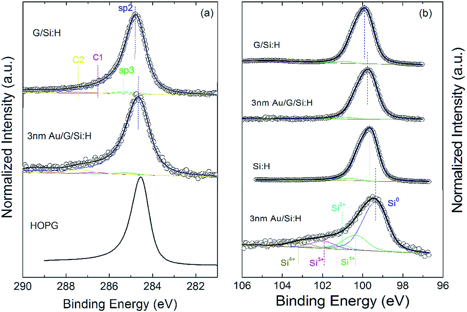 | ||
| Fig. 1 (a) C 1s core level spectra of G/Si:H before and after 3 nm Au deposition. The C 1s level of HOPG is also shown. (b) Si 2p core level spectra of Si:H and G/Si:H before and after 3 nm Au deposition. | ||
As gold is sequentially deposited on the G/Si sample, the position of the C 1s core level gradually shifts towards lower BE. This is assigned to gradual p-doping induced by charge transfer from Si to Au.9Fig. 2 shows the energy difference between the Fermi level and the Dirac point in graphene as well as the SBH of Si as a function of Au coverage. The Fermi level shifts from −0.25 ± 0.05 eV from the Dirac point before to −0.38 ± 0.05 eV after a 3 nm thick Au layer deposition (the negative sign indicates p-type doping).
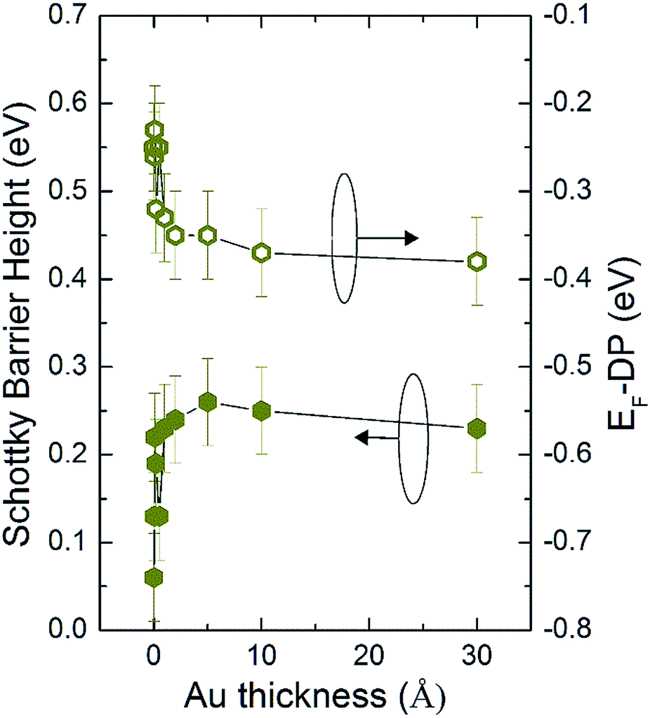 | ||
| Fig. 2 Schottky barrier height of Si and energy difference between the Dirac point and the Fermi level in the graphene layer as a function of Au coverage. | ||
The top curve in Fig. 1b shows the Si 2p core level for G/Si:H. An almost complete removal of SiO2 through the graphene layer is observed after the HF treatment. When present, the remaining silicon oxide thickness deduced from the ratio of Si4+ (located at 3.75 eV from the Si 2p3/2 peak) to Si-bulk components26 is estimated to be less than about 0.1 nm. The BE position of the Si 2p3/2 core level leads to a SBH of 0.06 ± 0.05 eV (see the ESI† for SBH determination). For the bare Si:H surface the BE position corresponds to a SBH of 0.30 ± 0.05 eV for a similar doping concentration.
A large discrepancy can be found in the literature for the G/Si SBH (from 0.32 to 0.89 eV (ref. 11 and 27–35)). Nevertheless, the SBH of our SLG/Si:H junctions determined by XPS is very low. Most results from the literature showing a higher SBH were obtained by transport measurements. In this case, hot spots due to defects or ripples may dominate the electrical transport through the junction and may reflect the electrical properties of only a small proportion of the junction surface. Other parameters such as the efficiency of hydrogen passivation, the residual silicon oxide under the graphene sheet or the graphene transfer quality may differ from sample to sample. In contrast, the photoemission experiment gives an averaged value of the SBH at a macroscopic scale and is widely insensitive to microscopic defects. Nevertheless, other reasons may explain the difference between our results and those of the literature as we will see in the next paragraph.
In the simple Schottky–Mott model, the SBH ϕB is the difference between the work function of graphene WG and the electronic affinity of the SC χSi:
| ϕB = WG − χSi |
The commonly used work function of graphene is 4.54 eV and the electronic affinity of Si is 4.05 eV. This would give rise to a ϕB of 0.49 eV, much larger than our measured SBH of 0.06 eV. However, for CVD graphene deposited via the PMMA assisted method, the work function was measured by Lin et al. to be WG = 4.3 eV, lower than the commonly used 4.54 eV because of resist contamination and structural defects induced during wet transfer.36 This would lead to an expected SBH of 0.25 eV. Moreover, a reduction of the SBH is expected for Si:H because of an electric dipole H−δq–Si+δq at the Si surface. A reduction of 0.21 eV was measured for Pb/n-Si:H compared to Pb/n-Si.37 A similar 0.21 eV reduction would lead to a SBH of 0.04 eV. This value is very close to the SBH we measure here. Our particularly low barrier may therefore be explained by the low work function of wet transferred CVD-graphene and the surface dipole. A better graphene quality and the absence of hydrogen passivation are expected to lead to a larger SBH.
With Au sequentially deposited, the Schottky barrier forms and the position of the bulk Si 2p component gradually shifts towards lower BE. For the uncovered sample, a 0.39 eV shift of the Si 2p core level is observed after 3 nm Au deposition giving rise to a final SBH of 0.66 ± 0.05 eV, slightly lower than the 0.75 ± 0.04 eV measured by Grupp and Taleb-Ibrahimi.38 Several Si 2p components are needed to fit the Si 2p peak for the Au/Si sample. These peaks are attributed to surface components induced by Si diffusion through Au and subsequent oxidation.39
For the graphene-covered sample, the position of the bulk Si 2p component gradually shifts towards lower binding energy after 3 nm Au deposition giving rise to a final SBH of 0.23 ± 0.05 eV, as shown in Fig. 2. This SBH is stable after 5 Å Au deposition. No reaction component is needed to fit the Si 2p core level. This result indicates that graphene is an efficient barrier against metal diffusion as already pointed out by several groups.7,8,40 The evolution of the SBH and doping concentration in the graphene layer as a function of Au coverage is presented in Fig. 2. As the FL in graphene shows a downshift of 0.13 ± 0.05 eV from the Dirac point with increasing gold coverage, the SBH shows an almost similar upshift of 0.17 ± 0.05 eV. These variations demonstrate the absence of pinning at the G/Si:H interface.
Capacitance–voltage (C–V) and current density–voltage (J–V) measurements were carried out to confirm the XPS results and determine the transport mechanism. A voltage bias across the Schottky barrier is able to modulate the depletion region width w and to change the charge located at the junction, making it behave as a parallel plate capacitor. When a small AC voltage δV is added to the reverse DC bias (V < 0), the junction shows a capacitive behavior with capacitance per unit area expressed as  where εs is the dielectric constant of Si, ND is the doping concentration, φi is the surface potential, V is the applied voltage, q is the electronic charge, kB is the Boltzmann constant and T is the temperature. A plot of 1/C2versus V should therefore be a straight line with the slope being 2/qεsND and the intercept being proportional to φi − kT/q. The built in potential φi is related to the SBH as
Fig. 3a shows the 1/C2versus V plot obtained at 1 MHz for different temperatures. The curves show straight parallel lines for V < 0. This is indicative of good quality Schottky junctions with a low density of interface states41 and a doping concentration independent of temperature. Fig. 3b shows the SBH ϕB deduced from these measurements as a function of temperature from 0.30 eV at 250 K down to 0.25 eV at 330 K. These results are in good agreement with the SBH deduced from XPS.
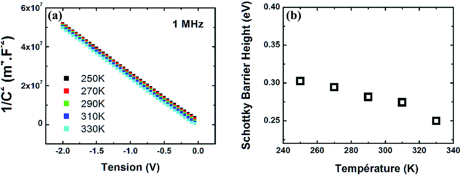 | ||
| Fig. 3 (a) 1/C2vs. V plot at 1 MHz for a Au/G/Si:H junction between 250 K and 330 K. (b) Schottky barrier height deduced from the capacitance–voltage measurements as a function of temperature. | ||
Fig. 4a shows the measured I–V characteristics between 220 K and 320 K. Non-linear rectifying behavior was observed for all the devices indicating thermionic emission (TE) dominated transport over the barrier. A significant increase in reverse current density was observed as the temperature raised from 220 K to 320 K. This is consistent with the reduction of the effective barrier height observed from C–V in Fig. 3b. The forward bias current density shows temperature dependence as well. The I–V characteristic of a Au contact on Si outside the G-covered area at 300 K is also shown for comparison.
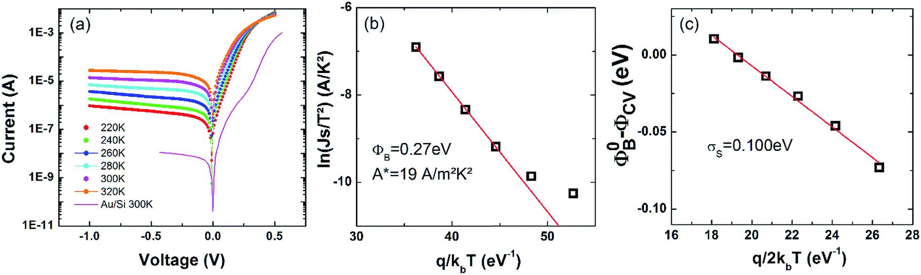 | ||
| Fig. 4 (a) Current–voltage measurements between 220 K and 320 K for Au/G/Si:H. The room temperature I–V characteristic of a Au/Si contact is also shown. (b) Richardson plot of the Au/G/Si:H junction and (c) determination of the standard deviation from the mean barrier height. | ||
The zero-bias Schottky barrier height,ϕ0B, and the ideality factor n at room temperature (RT) can be extracted using (TE) theory according to the following equation:
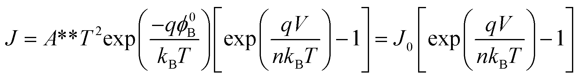 | (1) |
This plot is well fitted with a straight line between 260 and 320 K. The deviation from linearity below 260 K indicates a temperature dependent barrier height. The slope of such a plot gives ϕB = 0.27 eV, the effective SBH which is consistent with the barrier height of 0.23 eV measured by XPS and 0.28 eV by C–V at room temperature. The intercept gives an effective Richardson constant A** of 19 A m−2 K−2, 5 orders of magnitude lower than the expected A** for Si(001). Most reports on G/Si Schottky barriers show similarly low Richardson constants.42–45 This was attributed to the finite density of states in graphene and 2D massless Dirac fermion characteristics of its carriers29 or to inhomogeneous SBHs due to potential fluctuations at the interface.
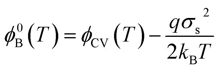
For the latter case, these fluctuations are described through the Werner model46 which correlates the mean ϕCV(T) and the apparent barrier ϕ0B(T):
 | (2) |
 and gives a standard deviation of σs = 100 meV.
Experimental confirmation of this model was realized with conductive-probe atomic force microscopy (CP-AFM). Fig. 5a shows an AFM scan of the edge of a 30 nm Au contact at the interface between uncovered and G-covered Si. CP-AFM mapping of the same area is shown in Fig. 5b. Four different interfaces can be seen in this picture at a bias voltage of –2 V: G/Si, Si, Au/G/Si and Au/Si. Note that the regions unprotected by gold were oxidized with a UV/ozone step. The Au/Si contact shows a large homogeneous local resistance in the 1013 Ω range (see the resistance histograms in ESI Fig. S3†) probably due to both the large SBH expected for Au/Si Schottky contacts and the diffusion of Si through the Au layer plus subsequent oxidation at the surface. When the graphene layer is present at the interface between Au and Si, we observe a strong reduction of local resistance consistent with the low SBH observed by XPS, C–V and J–V. Most of the surface shows a local resistance in the 104 to 106 Ω range with small areas of larger resistance in the 1010 Ω range. These local high resistive spots of ∼1010 Ω are related to the topography and are therefore attributed to resist residues. If we consider the local resistance to be dominated by the SBH at the interface, these measurements confirm that the Au/G/Si SBH is low and inhomogeneous with a Gaussian distribution centered at 104 Ω, our detection limit.
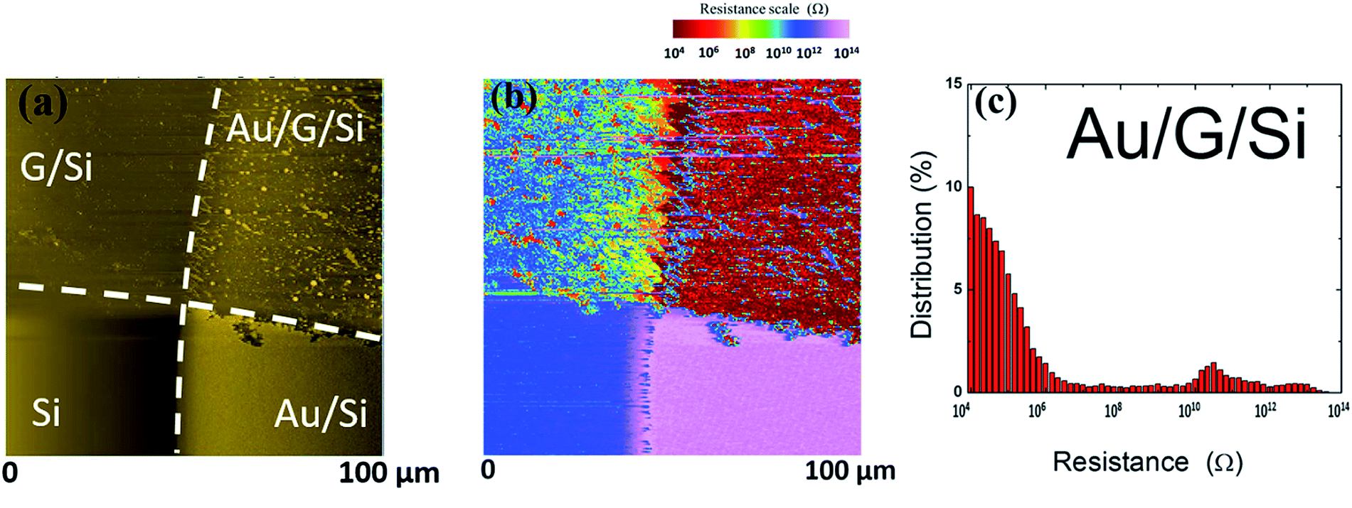 | ||
| Fig. 5 (a) AFM close-up showing the four regions, (b) ResiScope mapping at the interface between uncovered and G covered Si under 30 nm Au, and (c) resistance distribution in the Au/G/Si area. | ||
Conclusions
We studied Au/G/Si heterojunctions by different techniques so as to determine their interface physico-chemistry, band alignments, homogeneity and electrical transport characteristics. We observed by XPS successful Si oxide removal after graphene transfer and an absence of intermixing between Si and Au. XPS was also used to determine the band alignments: for G/Si:H, the Si SBH is close to zero and the progressive increase of graphene p-doping by Au induces a similar progressive increase of the Si SBH which means that FL pinning was alleviated at the surface. Multiscale transport techniques confirmed the SBH value of Au/G/Si:H in the 0.25 eV range at room temperature and identified thermionic emission as the dominant transport process. The Richardson constant was very low compared to the expected value for ideal Metal/Si Schottky junctions. This low value was attributed to an inhomogeneous SBH as confirmed by CP-AFM imaging. These results show that, in order to form a low resistance contact between Si and graphene, an appropriate choice of metal is necessary. This metal should induce n-type doping of the graphene sheet in order to further reduce the SBH on the Si side and to form a low resistance contact with graphene.Conflicts of interest
The authors declare no competing financial interest.Acknowledgements
The authors acknowledge Bruno Bêche for his help with AFM measurements and ANR grant ENSEMBLE for financial support. We thank the SIR platform of ScanMAT at Univ. Rennes 1 for technical support for the Raman measurements.References
- W. Mönch, J. Vac. Sci. Technol., B: Microelectron. Process. Phenom., 1988, 6, 1270 CrossRef.
- Y. Zhou, M. Ogawa, X. Han and K. L. Wang, Appl. Phys. Lett., 2008, 93, 202105 CrossRef.
- S. Gupta, P. Paramahans Manik, R. Kesh Mishra, A. Nainani, M. C. Abraham and S. Lodha, J. Appl. Phys., 2013, 113, 1–7 Search PubMed.
- M. Y. Ali and M. Tao, J. Appl. Phys., 2007, 101, 103708 CrossRef.
- M. H. Lee, Y. Cho, K. E. Byun, K. W. Shin, S. G. Nam, C. Kim, H. Kim, S. A. Han, S. W. Kim, H. J. Shin and S. Park, Nano Lett., 2018, 18, 4878–4884 CrossRef CAS PubMed.
- S.-G. Nam, Y. Cho, M.-H. Lee, K. W. Shin, C. Kim, K. Yang, M. Jeong, H.-J. Shin and S. Park, 2D Mater., 2018, 5, 041004 CrossRef.
- C. P. Y. Wong, T. J. H. Koek, Y. Liu, K. P. Loh, K. E. J. Goh, C. Troadec and C. A. Nijhuis, ACS Appl. Mater. Interfaces, 2014, 6, 20464–20472 CrossRef CAS PubMed.
- J. Hong, S. Lee, S. Lee, H. Han, C. Mahata, H.-W. Yeon, B. Koo, S.-I. Kim, T. Nam, K. Byun, B.-W. Min, Y.-W. Kim, H. Kim, Y.-C. Joo and T. Lee, Nanoscale, 2014, 6, 7503–7511 RSC.
- G. Giovannetti, P. Khomyakov, G. Brocks, V. Karpan, J. van den Brink and P. Kelly, Phys. Rev. Lett., 2008, 101, 026803 CrossRef CAS PubMed.
- P. A. Khomyakov, G. Giovannetti, P. C. Rusu, G. Brocks, J. Van Den Brink and P. J. Kelly, Phys. Rev. B: Condens. Matter Mater. Phys., 2009, 79, 195425 CrossRef.
- H. Yang, J. Heo, S. Park, H. J. Song, D. H. Seo, K.-E. Byun, P. Kim, I. Yoo, H.-J. Chung and K. Kim, Science, 2012, 336, 1140–1143 CrossRef CAS PubMed.
- K.-E. Byun, S. Park, H. Yang, H.-J. Chung, H. J. Song, J. Lee, D. H. Seo, J. Heo, D. Lee, H. J. Shin and Y. S. Woo, 2012 IEEE Nanotechnol. Mater. Devices Conf., 2012, pp. 63–66 Search PubMed.
- O. M. J. van't Erve, A. L. Friedman, E. Cobas, C. H. Li, a. T. Hanbicki, K. M. McCreary, J. T. Robinson and B. T. Jonker, J. Appl. Phys., 2013, 113, 17C502 CrossRef.
- O. M. J. van't Erve, a L. Friedman, E. Cobas, C. H. Li, J. T. Robinson and B. T. Jonker, Nat. Nanotechnol., 2012, 7, 737–742 CrossRef PubMed.
- X. Zhu, S. Lei, S. H. Tsai, X. Zhang, J. Liu, G. Yin, M. Tang, C. M. Torres, A. Navabi, Z. Jin, S. P. Tsai, H. Qasem, Y. Wang, R. Vajtai, R. K. Lake, P. M. Ajayan and K. L. Wang, Nano Lett., 2018, 18, 682–688 CrossRef CAS PubMed.
- K.-E. Byun, H.-J. Chung, J. Lee, H. Yang, H. J. Song, J. Heo, D. H. Seo, S. Park, S. W. Hwang, I. Yoo and K. Kim, Nano Lett., 2013, 13, 4001–4005 CrossRef CAS PubMed.
- I. Goykhman, U. Sassi, B. Desiatov, N. Mazurski, S. Milana, D. De Fazio, A. Eiden, J. Khurgin, J. Shappir, U. Levy and A. C. Ferrari, Nano Lett., 2016, 16, 3005–3013 CrossRef CAS PubMed.
- M. P. Seah, Surf. Interface Anal., 1989, 14, 488 CrossRef CAS.
- F. J. Himpsel, G. Hollinger and R. A. Pollak, Phys. Rev. B: Condens. Matter Mater. Phys., 1983, 28, 7014–7018 CrossRef CAS.
- O. Schneegans, P. Chrétien and F. Houze, Patents WO 2011/138738, 2011.
- P. Narchi, J. Alvarez, P. Chrétien, G. Picardi, R. Cariou, M. Foldyna, P. Prod'homme, J. P. Kleider and P. R. i. Cabarrocas, Nanoscale Res. Lett., 2016, 11, 1–8 CrossRef CAS PubMed.
- A. Nikitin, L.-Å. Näslund, Z. Zhang and A. Nilsson, Surf. Sci., 2008, 602, 2575–2580 CrossRef CAS.
- G. Cunge, D. Ferrah, C. Petit-Etienne, A. Davydova, H. Okuno, D. Kalita, V. Bouchiat and O. Renault, J. Appl. Phys., 2015, 118, 123302 CrossRef.
- Y.-C. Lin, C.-C. Lu, C.-H. Yeh, C. Jin, K. Suenaga and P.-W. Chiu, Nano Lett., 2012, 12, 414–419 CrossRef CAS PubMed.
- C. Lin, H. Shiu, L. Chang, C. Chen, C. Chang and F. S. Chien, J. Phys. Chem. C, 2014, 118, 24898–24904 CrossRef CAS.
- J. R. Shallenberger, D. a. Cole, S. W. Novak, R. L. Moore, M. J. Edgell, S. P. Smith, C. J. Hitzman, J. F. Kirchhoff, E. Principe, S. Biswas, R. J. Bleiler, W. Nieveen and K. Jones, 1998 Int. Conf. Ion Implant. Technol. Proc., (Cat. No. 98EX144), 1999, vol. 1, pp. 79–82 Search PubMed.
- S. Tongay, M. Lemaitre, X. Miao, B. Gila, B. R. Appleton and a. F. Hebard, Phys. Rev. X, 2012, 2, 011002 Search PubMed.
- S. Parui, R. Ruiter, P. J. Zomer, M. Wojtaszek, B. J. Van Wees and T. Banerjee, J. Appl. Phys., 2014, 116, 1–6 CrossRef.
- D. Sinha and J. U. Lee, Nano Lett., 2014, 14, 4660–4664 CrossRef CAS PubMed.
- X. An, F. Liu, Y. J. Jung and S. Kar, Nano Lett., 2013, 13, 909–916 CrossRef CAS PubMed.
- F. Liu and S. Kar, ACS Nano, 2014, 8, 10270–10279 CrossRef CAS PubMed.
- X. Miao, S. Tongay, M. K. Petterson, K. Berke, A. G. Rinzler, B. R. Appleton and A. F. Hebard, Nano Lett., 2012, 12, 2745–2750 CrossRef CAS PubMed.
- E. Shi, H. Li, L. Yang, L. Zhang, Z. Li, P. Li, Y. Shang, S. Wu, X. Li, J. Wei, K. Wang, H. Zhu, D. Wu, Y. Fang and A. Cao, Nano Lett., 2013, 13, 1776–1781 CrossRef CAS PubMed.
- H. Y. Kim, K. Lee, N. McEvoy, C. Yim and G. S. Duesberg, Nano Lett., 2013, 13, 2182–2188 CrossRef CAS PubMed.
- A. Singh, M. A. Uddin, T. Sudarshan and G. Koley, Small, 2014, 10, 1555–1565 CrossRef CAS PubMed.
- W.-H. Lin, T.-H. Chen, J.-K. Chang, J.-I. Taur, Y.-Y. Lo, W.-L. Lee, C.-S. Chang, W.-B. Su and C.-I. Wu, ACS Nano, 2014, 8, 1784–1791 CrossRef CAS PubMed.
- W. Mönch, Europhys. Lett., 1994, 27, 479–484 CrossRef.
- C. Grupp and A. Taleb-Ibrahimi, Phys. Rev. B: Condens. Matter Mater. Phys., 1998, 57, 6258–6261 CrossRef CAS.
- A. Cros and P. Muret, Mater. Sci. Rep., 1992, 8, 271–367 CrossRef CAS.
- J. C. Le Breton, S. Tricot, G. Delhaye, B. Lépine, P. Turban and P. Schieffer, Appl. Phys. Lett., 2016, 109, 051601 CrossRef.
- S. J. Fonash, J. Appl. Phys., 1982, 54, 1966–1975 CrossRef.
- D. Tomer, S. Rajput, L. J. Hudy, C. H. Li and L. Li, Nanotechnology, 2015, 26, 215702 CrossRef CAS PubMed.
- S. Liang, W. Hu, A. Di Bartolomeo, S. Adam and L. K. Ang, IEEE Int. Electron Devices Meet., 2016, 14.4.1–14.4.4 Search PubMed.
- D. P. Sinha and J. U. Lee, Nano Lett., 2014, 14, 4660–4664 CrossRef CAS PubMed.
- A. Di Bartolomeo, F. Giubileo, G. Luongo, L. Iemmo, N. Martucciello, G. Niu, M. Fraschke, O. Skibitzki, T. Schroeder and G. Lupina, 2D Mater, 2017, 4, 015024 CrossRef.
- J. H. Werner and H. H. Güttler, J. Appl. Phys., 1991, 69, 1522–1533 CrossRef CAS.
Footnote |
| † Electronic supplementary information (ESI) available: S1 – Graphene transfer protocol; S2 – Schottky barrier height XPS determination; S3 – Raman spectrum of gold protected graphene; S4 – Optical image, AFM image and resistance histograms of the areas under study. See DOI: 10.1039/c9na00393b |
| This journal is © The Royal Society of Chemistry 2019 |