
 Open Access Article
 This Open Access Article is licensed under a Creative Commons Attribution-Non Commercial 3.0 Unported Licence
Monte Carlo simulation of nanoscale material focused ion beam gas-assisted etching: Ga+ and Ne+ etching of SiO2 in the presence of a XeF2 precursor gas†
Kyle T.
Mahady
 a,
Shida
Tan
b,
Yuval
Greenzweig
c,
Amir
Raveh
c and
Philip D.
Rack
*ad
a,
Shida
Tan
b,
Yuval
Greenzweig
c,
Amir
Raveh
c and
Philip D.
Rack
*ad
aUniversity of Tennessee, Knoxville, Tennessee 37996, USA. E-mail: prack@utk.edu
bIntel Corporation, Santa Clara, California 95054, USA
cIntel Israel, Haifa 31015, Israel
dCenter for Nanophase Materials Science, Oak Ridge National Laboratory, Oak Ridge, Tennessee 37831, USA
First published on 30th July 2019
Abstract
Elucidating energetic particle-precursor gas–solid interactions is critical to many atomic and nanoscale synthesis approaches. Focused ion beam sputtering and gas-assisted etching are among the more commonly used direct-write nanomachining techniques that have been developed. Here, we demonstrate a method to simulate gas-assisted focused ion beam (FIB) induced etching for editing/machining materials at the nanoscale. The method consists of an ion–solid Monte Carlo simulation, to which we have added additional routines to emulate detailed gas precursor–solid interactions, including the gas flux, adsorption, and desorption. Furthermore, for the reactive etching component, a model is presented by which energetic ions/target atoms, and secondary electrons, transfer energy to adsorbed gas molecules. The simulation is described in detail, and is validated using analytical and experimental data for surface gas adsorption, and etching yields. The method is used to study XeF2 assisted FIB induced etching of nanoscale vias, using both a 35 keV Ga+, and a 10 keV Ne+ beam. Remarkable agreement between experimental and simulated nanoscale vias is demonstrated over a range of experimental conditions. Importantly, we demonstrate that the resolution depends strongly on the XeF2 gas flux, with optimal resolution obtained for either pure sputtering, or saturated gas coverage; saturated gas coverage has the clear advantage of lower overall dose, and thus lower implant damage, and much faster processing.
1 Introduction
Controlling/editing materials at the nanoscale is critical for the realization of many emerging technologies. One synthesis technique for sculpting materials at the nanoscale is focused ion beam (FIB) nanomachining. FIBs are used in many applications, ranging from imaging with the helium ion microscope (HIM),1–3 ion beam induced deposition,4–6 and, nanomachining.7,8 Owing to the high achievable beam resolutions using the gas field ionization source (GFIS), FIBs using light ions, such as Ne+ and He+, have attracted significant attention in recent years. However, a draw back of nanomachining performed using FIB sputtering is that it requires sufficiently high ion doses to sputter material from the target surface, which may produce significant subsurface damage.9 Subsurface damage may be mitigated through the use of focused ion beam induced etching (FIBIE); in FIBIE, a reactive precursor gas, such as XeF2 is used to enhance the material removal rate, which therefore reduces the required dose. However, the factors determining resolution for FIB sputtering are not perfectly known, and the addition of a precursor gas further influences achievable nanomachining resolutions in a way which is dependent on the interaction of the gas flux, and scan parameters. In this paper, we describe a Monte Carlo simulation for FIBIE with XeF2, and use it to study the resolution of etched features in SiO2.FIBIE reduces the subsurface damage associated with nanomachining by enhancing material removal rate, and thereby reducing the total ion dose required. Damage to the substrate may result from high doses of energetic ions, in the form of implanted ions in the subsurface (which may result in, for example, bubbling9), as well as implanted energy, which may cause such effects as amorphization of a crystalline target.8,10 FIBIE works similarly to electron beam induced etching: a reactive precursor gas is injected near the substrate, which then adsorbs to the surface as a monolayer. In the case of SiO2 with a XeF2 precursor, the gas does not spontaneously etch; however, the input of energy from the ion beam leads to dissociation of adsorbed molecules. The volatile compounds resulting from the dissociation of the XeF2 molecule, and reaction with the substrate, may be removed from the substrate spontaneously, or by additional interactions resulting from the ion beam.
While atomic layer control via FIB sputtering and etching has not been achieved (see ref. 11 for a recent perspective/review on atomic scale fabrication), the reduced sub-surface scattering that occurs in 2D materials provide avenues for enhanced resolution. In this regard, we have explored controlled defect introduction via scanning He+ irradiation in multilayer12 and single layer13 WSe2. Additionally, subsurface nanoscale nanomachining via laser-assisted He+ focused ion beam sputtering was shown to enhance the etching rate in single layer graphene nanochannels.14
Monte Carlo method simulations are widely used to study interactions of energetic ions with solid targets, and FIB processing specifically. Such applications include studying subsurface damage,9,15,16 imaging with the HIM,17 and ion beam induced deposition.18 One of the most popular Monte Carlo programs is SRIM,19,20 which simulates the interaction of numerous ion species and target compositions. However, despite its versatility and widespread use, SRIM is unable to simulate the effects of cumulative material removal due to either sputtering, or gas assisted etching. While several Monte Carlo methods have been developed which incorporate target evolution due to sputtering,21–24 we are unaware of any simulation that fully accounts for both sputtering, and material removal due to FIBIE. For this reason, we have developed the EnvizION Monte Carlo code, which has been previously used to simulate FIB milling,25–29 and secondary electron (SE) emission.30 While chemically assisted etching was estimated previously using EnvizION,31 this was emulated by reducing the surface binding energy of the target material, and was not sufficient to understand all factors related to material removal rate, as well as etching resolution. In this paper, we introduce our method for simulating gas assisted etching using EnvizION; this method incorporates details about the incoming gas flux, population of irregular surface features with gas, and depletion of gas due to reaction with substrate surface atoms driven by energy added from the ion beam. While specifically developed for high-energy focused ion beam applications, low-energy variants to the energy transfer could be implemented for atomic layer etching, as well as the inverse plasma enhanced atomic layer deposition.
The ion solid interaction of the EnvizION simulation method is based closely on SRIM.19,20 Unlike SRIM, EnvizION employs a voxel based representation of the computational domain, which permits the target to evolve as material is sputtered, and redeposited elsewhere. Bulk relaxation, and surface smoothing routines are employed to reduce porosity, and other simulation artifacts, during sputtering. The excitation and emission of SEs by the primary ion may additionally be simulated, according to the type of substrate. The FIBIE method, presented in this paper, consists of a method for simulating both the incoming gas flux, as well as the interactions by which the primary ion beam may cause dissociation of adsorbed XeF2, and the associated etching of material. The mechanism by which the ions trigger dissociation of adsorbed XeF2 is modeled similarly to the atomistic mechanism of ion beam induced deposition described by Dubner.32,33 In this model, the interaction between the primary ion and the adsorbed surface molecules is mediated by the substrate. The primary ion generates large numbers of displaced atoms in the near surface region of the target; some of these displaced atoms may reach the surface of the target, where they are permitted to interact with adsorbed gas through a binary collision. In contrast to Dubner's model, we additionally allow secondary electrons to cause dissociation with an energy dependent cross section.
In Section 2, we describe the simulation method in detail. Section 3 compares simulations with experiments for five sets of scan parameters for Ga+ etching, and three sets of scan parameters for Ne+ etching. We study the etching resolution with respect to gas flux in Section 4, and our results are summarized in Section 5.
2 Simulation method
In this section, we survey the novel aspects of the method for simulating FIBIE of SiO2 with a XeF2 precursor. Details of the sputtering method have been presented previously, with studies focusing on the validation of the code, and sputtering in monatomic substrates,28 and the use of simulations to understand sputtering in SiO2 targets.29 Monte Carlo modeling of SE emission was previously implemented only for conducting targets;30 in the present work, we use a similar method, but with the electron scattering determined by interaction with optical phonons, using the Monte Carlo method of.34 In contrast, the method described in our previous work30 for conducting targets was based on the inelastic interactions of excited electrons with other electrons. The SiO2 Monte Carlo method for SE emission that we employ does not account for charging of the substrate; this subject will be studied in the near future.In this paper, we study line scans, which consist of a discrete set of “pixels”, with length Lscan, and with pixel spacing or “pitch” Δx; the ion beam dwells at each pixel center for a time τdwell, before moving to the next pixel center. The number of pixels in a single line, Lscan/Δx, defines a “frame”. After a frame is scanned, the experiment may pause or blank the beam for some time to allow the gas flux to repopulate the surface with XeF2; this time is referred to as the “refresh time”, denoted τrefresh. After refreshing, another frame is etched by scanning the beam back along the line (i.e., we study “serpentine” scans, though any patterning option is possible). This process continues until the full dose has been reached (generally on the order of thousands of frames for the experiments presented in this paper).
The computational domain consists of the region
| {(x, y, z): xmin < x < xmax, ymin < y < ymax, z ∈ (−hmax, hpad)} |
All substrates that we consider here consist of SiO2, initially occupying the region z < 0. The empty space at the top of the domain is taken to be hpad = 25 nm, and xmin, xmax, ymin, ymax, and hmax, vary by simulation. The domain is represented by a 3D cubic lattice of voxels, with the centers of each voxel separated by a distance δ ≈ 0.25 nm, with δ being the average distance between atomic centers in SiO2. Each voxel is represented by a flag which corresponds to the contents of the voxel, either empty, or occupied by an atom of Si, O, or an implanted neutral atom of the impinging ion type; the initial substrate is populated at random with 1/3 Si and 2/3 O voxels. Ga+ ions are assumed to occupy lattice sites after coming to a rest in the target, while Ne+ ions are assumed to either occupy interstitial locations, or to diffuse and escape from the target; this is modeled by depositing stopped Ga+ ions in the nearest empty voxel, while Ne+ ions are removed from the computational domain after coming to a rest. The SiO2 sputtering simulation method is described in detail in our previous work.29 For all simulations considered here, we use “mirror” boundary conditions: if a moving ion, recoil atom, or gas molecule, with direction of travel ![[V with combining right harpoon above (vector)]](https://www.rsc.org/images/entities/i_char_0056_20d1.gif) , reaches the x or y boundaries, its direction of travel is set to
, reaches the x or y boundaries, its direction of travel is set to
← − 2(·![[n with combining right harpoon above (vector)]](https://www.rsc.org/images/entities/i_char_006e_20d1.gif) ) ) |
is the outward pointing normal of the boundary. In previous versions of EnvizION,28,29 the simulation had open boundary conditions so that moving ions and target atoms which leave the simulation domain are no longer tracked. Open boundary conditions can lead to significant artifacts in via depth if the domain is not large enough, and are problematic for the gas simulation, as discussed below.
The method that we employ for gas assisted etching (GAE) is based on that described by Dubner32 for modeling ion beam induced deposition. In this model, the precursor gas (in our case, XeF2) is assumed to follow a Langmuir isotherm on the SiO2 surface. Once adsorbed, the XeF2 does not etch spontaneously, but remains adsorbed for its residence time (100 ms), or until it is activated, either directly or indirectly, by the ion beam. Once etching occurs, the simulation emulates the chemical reaction as follows:
| SiO2 + 2XeF2 → SiF4 + O2 + 2Xe | (1) |
The etch products are assumed to immediately volatilize, and are removed from the substrate. The method for simulating gas assisted etching (GAE) consists of two components:
(1) A method for the population of the surface with gas molecules.
(2) A method for the ion beam to activate the adsorbed gas to etch.
Diffusion of the adsorbed XeF2 along the surface may be important for both the etch rate and the resolution of etched vias; however, it is computationally costly, and we ignore diffusion in the present study.
In simulations, the surface is populated by an isotropic gas flux, with gas molecules adsorbing to the surface following a Langmuir isotherm model. Each gas molecule may occupy exactly one surface site, which in simulations is defined as an empty voxel which has at least one nearest or next-nearest neighbor voxel which contains a substrate atom. While surface sites and adsorption orientations are not distinguished in this version of the simulation, for systems where atom specific and molecular orientation specific orientations are known, we can accommodate these specifics with modified residence times and dissociation energies.
We illustrate the isotropic gas population routine in Fig. 1. The population of the surface by gas molecules is simulated as an isotropic flux. For each gas molecule, an initial position P is generated uniformly at z = hpad, and an initial trajectory V is generated from the half sphere of trajectories with z component less than zero. The gas molecule then travels according to the following steps:
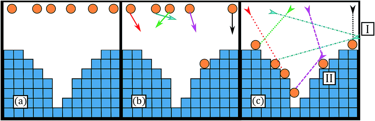 | ||
| Fig. 1 Two dimensional schematic of the gas population routine. (a) Gas molecule positions are generated from a uniform distribution at the top of the domain. (b) Trajectories are assigned to each molecule from a uniform distribution over a half sphere. (c) Molecules move line-of-sight until they find an empty site to adsorb to, permitting mirror boundary conditions (I) and gas ricochet (II). | ||
function gas recoil (P, V)
it ← 0
while (it < itmax) do
(1) Trace a ray from P along V until either a surface site is reached, or we reach the boundary z = hpad or z = −hmax. If a boundary is reached, the routine terminates. Otherwise, let the position of the surface site be given by P′.
(2) If the surface site is empty, generate a uniform random number r ∈ (0, 1). If r < α, the gas molecule adsorbs to the surface site at P′.
(3) For all other cases, generate a new random trajectory V′, and update the molecule's position and trajectory with P ← P′, V ← V′.
(4) it ← it + 1.
end while
end function
The parameter α is referred to as the sticking coefficient, and expressed the probability that a gas molecule will adsorb to a site on which it is incident. During the ray trace step of gas recoil, it is important that open boundary domains are not used, as this will prevent gas trajectories with small z component from reaching the surface. Gas molecules that have adsorbed onto the surface may spontaneously desorb with a mean residency time τr, which we take to be 100 ms, following Harriott (1993).35 A gas molecule which desorbs at position Pdesorb is assigned a randomized trajectory Vdesorb, and we call gas recoil (Pdesorb, Vdesorb), i.e., desorbed gas molecules may recoil throughout the domain until either escaping, or re-adsorbing to an empty site. In simulations, the gas population routine is called between each pixel dwell, and during the gas refresh time. In the first case, after a pixel dwell of length τdwell, the gas flux is simulated for τdwell as well, before the next pixel is simulated. Dwell times are typically a few μs, or sub-μs, while the timescales characterizing gas population are on the order of thousands of μs, so that this simplification is expected to introduce little error.
To understand the population of a surface due to the setup we have described, it is helpful to compare the gas population of an irregular surface with that of a perfectly flat surface. For a flat surface, in the absence of diffusion or ion beam induced dissociation, our gas population scheme is described by the following equation:
| ρ(t) = ρ∞ + (ρ0 − ρ∞)exp(−tτa−1) | (2) |
| τa−1 = ϕδ2 + τr−1 | (3) |
| ρ∞ = ϕτa | (4) |
 . The effective gas flux, in molecules per area per unit time, is given by ϕ. Fig. 2(a) plots the gas fraction as a function of time for an initial flat substrate with zero gas population, for varying gas flux. When the gas flux is as high as 1018 molecules per cm2 per s, the gas fraction rapidly approaches full coverage. Importantly, in the experiments we consider here, we are interested in the formation of high aspect ratio valleys, which populate quite differently than a flat surface. Fig. 2(b) compares the population of the flat surface from eqn (2), to the simulated result using the described gas recoil routine in a rotationally symmetric Gaussian via exposed to a gas flux of 1017 molecules per cm2 per s; this Gaussian via has a 15 nm full width at half maximum (FWHM), and a depth of 100 nm. While the simulated population at the top of the via and the surrounding flat surface (z = 0) is the same as the analytical theory, deeper in the via we see that gas population occurs much more slowly; near the via bottom (z = −99 nm) gas population occurs on a timescale that is more than two orders of magnitude slower than the flat surface.
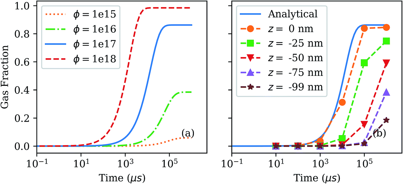 | ||
| Fig. 2 (a) Population of a flat surface due to a variable isotropic gas flux, calculated using the eqn (2). (b) Population of a 100 nm deep, 15 nm FWHM Gaussian via at various depths. The analytical result for a flat surface is shown by the solid line. The dashed lines in (b) are shown to help guide the eye. | ||
An important component of the gas recoil routine is that a gas molecule which fails to adsorb to the surface spontaneously desorbs with a random trajectory; this emulates transient adsorption to an already adsorbed gas molecule, or a failure to adsorb due to a sticking coefficient less than one. After desorbing, a gas molecule recoils throughout the domain, which, for brevity, we refer to as a gas ricochet. We consider the effects of ignoring ricochet in Fig. 3. Fig. 3(a) shows a top down view of the simulated gas fraction in Fig. 2(b) at t = 106 μs, while Fig. 3(b) shows the same simulation, except not permitting ricochet (i.e., if a gas molecule reaches an already occupied gas site, the gas recoil routine for that molecules stops, and the gas molecule disappears); in this manner gas sites are only populated in proportion to the solid angle exposed to the top of the domain. Ignoring ricochet results in a significantly lower gas fraction. Fig. 3(c) plots the gas fraction from Fig. 3(a) and (b), at various times and depths in the via; we can see in particular that the gas population with ricochet becomes higher relative to the simulation without ricochet as the gas fraction increases. This can be understood as follows: as the gas fraction inside of a via increases, this leads to more incident gas molecules landing on already full surface sites, and therefore subsequent desorption allows gas molecules to find non-occupied sites; this contribution is a critical component to populating high-aspect ratio vias, where direct adsorption is minimal due to the low solid angle relative to the top of the domain.
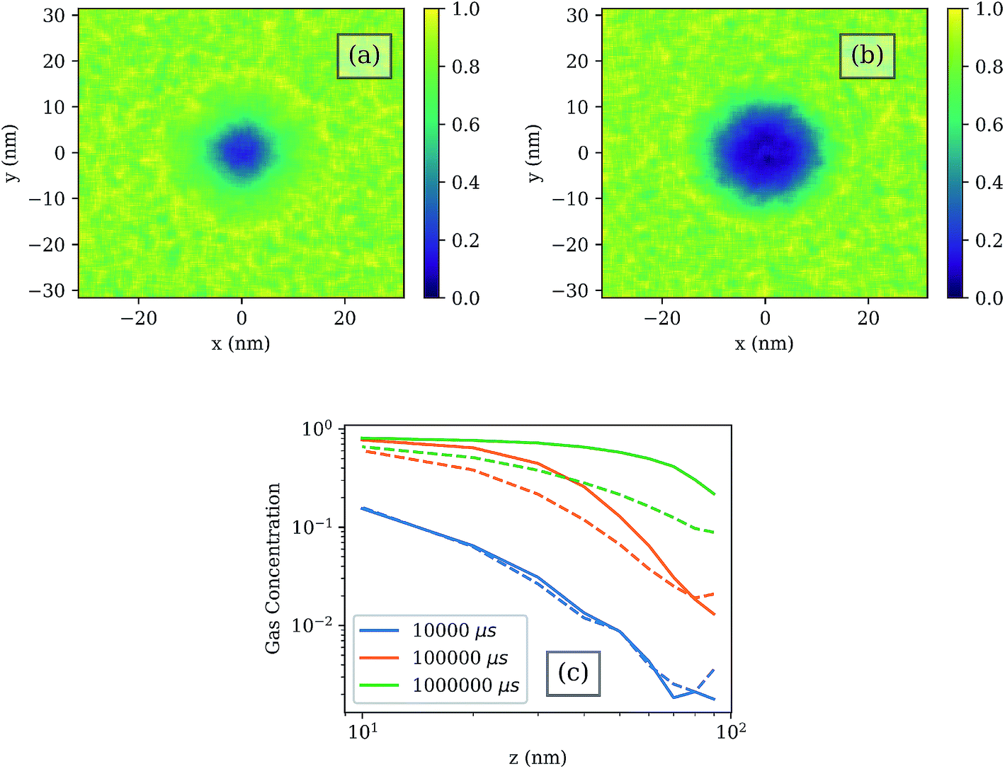 | ||
| Fig. 3 Population in a 100 nm deep, 15 nm FWHM Gaussian via. The fraction of gas sites occupied after 1 × 10⁶ μs, with a 1017 molecules per cm2 per s gas flux, is shown for (a) allowing gas molecules to ricochet, and (b) not allowing gas molecules to ricochet. Plots show a top-down view of the gas concentration. (c) shows the fraction of all gas sites occupied, as a function of depth, for these same vias; the refresh time is varied, and the solid lines indicate gas populations obtained with ricochet, while the dashed lines indicate gas populations obtained without ricochet. | ||
The primary ion Monte Carlo which depends on the ion type (here Ne+ and Ga+) and the target substrate (here SiO2) proceeds as described in our previous work,29 which is in turn closely based on SRIM.20 Interested readers should refer to our previous work29 for the relevant SiO2 parameters that affect the ion–solid interactions, as we focus here on the precursor–solid interactions that are operative in the new simulation. Summarily, moving atoms (i.e., primary ions and recoiling target atoms) exhaust their energy through a combination of elastic collisions with atoms in the substrate, and inelastic interactions with the electrons of the substrate. Inelastic interactions may give rise to secondary electron emissions. Elastic collisions give rise to the scattering of moving atoms; if an elastic collision transfers more energy than a displacement threshold Edisp to the atom in the target, the target atom becomes a recoil, and travels through the substrate similarly to the incident ion. In the near surface region, Edisp = 0, while Edisp = 8 eV elsewhere. If a moving atom reaches the surface with energy greater than the surface binding energy Esurf, then it may be sputtered. Atoms which are not sputtered, and whose initial energy is less than 8 eV, are returned to their initial position after their energy drops to zero.
In the EnvizION model, gas-assisted etching is driven by interactions between moving atoms, excited electrons, and adsorbed XeF2. Any moving atom which reaches an occupied surface site is permitted to interact with the adsorbed XeF2 molecule – importantly, even if an atom with energy insufficient to sputter reaches the surface, it is permitted to interact with an adsorbed XeF2. If an electron reaches an occupied surface site, it etches with a probability Pe−. Secondary electron dissociation cross sections have been studied in detail for electron beam induced deposition,36–38 and electron beam induced etching studies.39,40 For simplicity, in what follows we set Pe− = 1; notably, even with a unit etching probability, we find that electron etching is a very minor component in ion beam induced etching.
Moving atoms interact with adsorbed XeF2 through a binary collision model (see Dubner32). The interaction between a moving atom A and an adsorbed XeF2 molecule is calculated as a binary collision between the moving atom, and one of the component atoms of the XeF2. There is a 1/3 chance that the collision is with the Xe, and a 2/3 chance that the collision is with a F atom; for convenience, we refer to the selected knock-on atom in the precursor gas molecule as B. The maximum impact parameter pmax is set to be rA + rB where rA and rB are the van der Waals radii of atoms A and B respectively. The impact parameter of the binary collision is then set to be 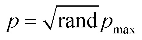 , where rand is uniformly distributed in (0, 1). If the amount of energy transferred from A to B exceeds an activation energy Eact, then dissociation and subsequent etching occurs. Based on eqn (1), if etching occurs, the simulation flags the nearest occupied voxel to empty, and then flags another nearest neighbor, or next-nearest neighbor, voxel to empty with probability 0.5. In this way, each gas molecule removes on average 1.5 atoms when it dissociates, in accordance with eqn (1). Note that the etching routine in simulations does not distinguish Si and O atoms, nor does it allow for two XeF2 molecules to participate in a reaction, and instead removes, on average, the correct number of substrate atoms per dissociated XeF2.
Based on the above discussion, there are two parameters whose values are unknown: the activation energy Eact, and the sticking coefficient α. By comparison with the experiments described in Section 3, and further experimental benchmarks described in the ESI,† we use an activation energy of Eact = 0.05 eV. We use a value of α = 1 for simulations; however the comparison with previously published experiments, presented in the ESI,† requires a value of α = 0.025 to account for the extremely high gas flux values in the experiments. The gas etching parameters used for simulations in this paper are summarized in Table 1.
| Parameter | Description | Value |
|---|---|---|
| τ r | Mean gas residence time on the surface | 100 ms |
| E act | Activation energy for XeF2 dissociation | 0.05 eV |
| D | Diffusion coefficient | 0 |
| P e−1 | Electron etching probability | 1 |
| α | Sticking coefficient | 1 |
Again, for computational efficiency, we ignore diffusion in all simulations. When XeF2 adsorbs to the surface, it may diffuse, similar to the case of IBID.41 In the present paper, we will ignore diffusion in all simulations. We will consider the effects of diffusion in a future paper, which, for 3D electron beam induced deposition studies, even short range diffusion has been shown to have interesting effects when transitioning from electron to mass transport limited regimes.42
3 Results
In Fig. 4, we illustrate etching due to 10 keV spot dwells of varying ion species. For these simulations, the gas fraction, or coverage, on the surface is kept at 1 during each simulation. These simulations were run without voxel updating, so that the surface remains smooth even if sufficient energy is transferred to a gas molecule to cause dissociation. He+ has a very low etch yield (5 atoms per ion) compared to Ne+ and Ga+ (21 and 35 atoms per ion, respectively). This is due to the fact that He+ travels deeper into the target, and generates few recoil atoms in the near surface region. Ne+ and Ga+ have similar etch yields, with Ga+ being significantly higher at this energy, due to the fact that it generates more recoils in general, as well as having an interaction volume nearer to the surface. However, the sputter yield varies greatly among the ion species, so that He+ ions show the greatest enhancement in material removal with XeF2, when compared to pure sputtering. The ratios of material removed with XeF2 to pure sputtering, per incident ion, are as follows: 38 for He+, 20 for Ne+, and 21 for Ga+. A histogram of the radial position of etch events is also shown in Fig. 4. Etch events occur within a few nanometers of the point of impact of the primary ion, determined by the number of recoil atoms generated in the near surface. Ne+ demonstrates the widest distribution of the three ions (see ESI† for additional details on the distribution of etch events).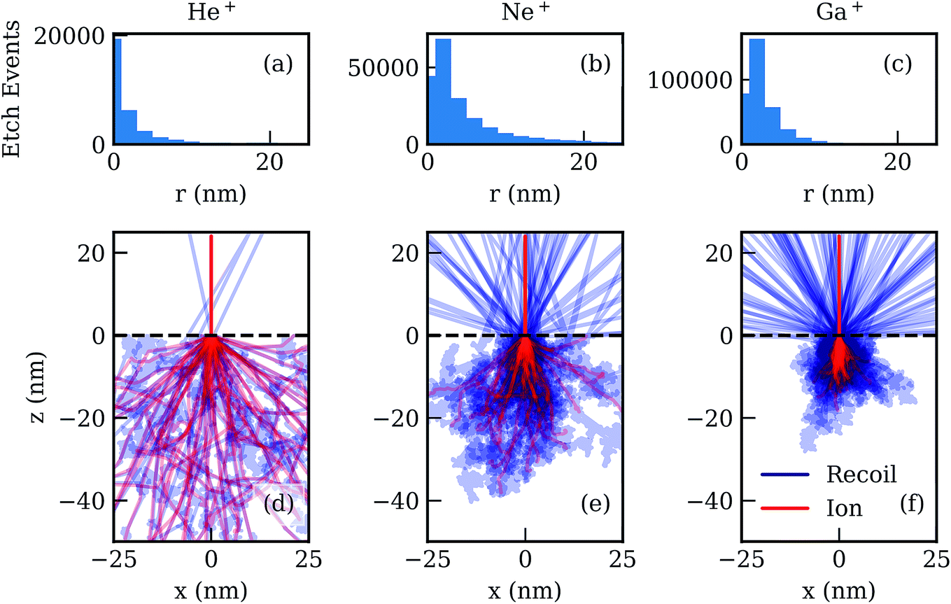 | ||
Fig. 4 Comparison of etching from 10 keV He+, Ne+, and Ga+ ion point dwells. Histograms of the radial location of all etch events are shown in (a)–(c), computed from 10![[thin space (1/6-em)]](https://www.rsc.org/images/entities/char_2009.gif) 000 incident ions. Ion paths are shown in red, and recoil atom paths are shown in blue, for 50 incident ions, in (d)–(f); the surface of the target is indicated by a dashed line. The etch yields for each ion are as follows: 4 atoms per ion for He+, 29 atoms per ion for Ne+, and 34 atoms per ion for Ga+. Note that (d)–(f) have projected all data along the y-axis, while simulations were three dimensional. 000 incident ions. Ion paths are shown in red, and recoil atom paths are shown in blue, for 50 incident ions, in (d)–(f); the surface of the target is indicated by a dashed line. The etch yields for each ion are as follows: 4 atoms per ion for He+, 29 atoms per ion for Ne+, and 34 atoms per ion for Ga+. Note that (d)–(f) have projected all data along the y-axis, while simulations were three dimensional. | ||
For the remainder of this section, we consider the application of the simulation method described in Section 2 to XeF2 assisted etching of SiO2 with Ne+ and Ga+ ion beams. Similar to our previous paper,29 we introduce “Effective Beam Profiles”, which describe the behavior of the ion beam profile, plus platform level artifacts which tend to reduce sputtering, and ion etching resolution. The functionality of the beam current distribution is derived from Tan et al.,8 where the x–y location of incoming ions is described by the following probability density:
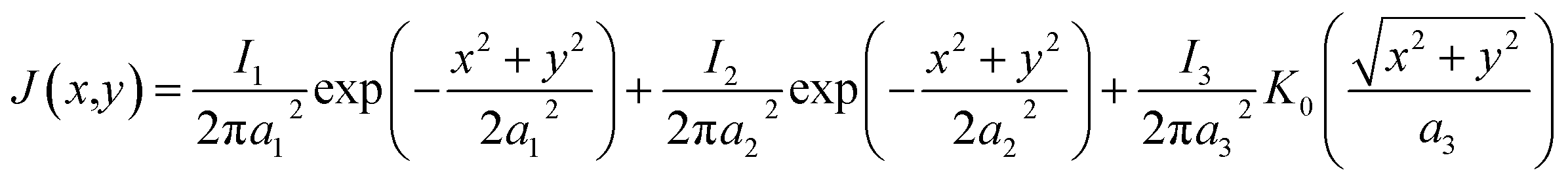 | (5) |
• Ga+ “Effective Beam”: (a1, a2, a3) = (9.44, 0, 55.64) nm, (I1, I2, I3) = (0.97, 0, 0.03)
• Ne+ “Effective Beam”: (a1, a2, a3) = (6, 27.9, 68.5) nm, (I1, I2, I3) = (0.89, 0.06, 0.05)
These beam profiles were derived by matching the shape of simulated etched vias to experiments; the true underlying functionality of the beam profile may differ from the precise functionality given here. We note that in both cases, these effective beams are larger than the measured beam profiles, but significantly narrower than the effective beam profiles reported in Mahady et al. (2018)29 for pure sputtering, suggesting that the lower doses associated with etching may reduce artifacts which broaden the sputtered/etched profile. We consider a comparison between the effective beam profiles here with those measured using the teardrop method of Tan et al.8 in the ESI.†
We study XeF2 assisted FIB etching using five scan parameter “recipes” for the Ga+ ion beam, and three for the Ne+ ion beam. The parameter setups are described in Table 2. The simulated scan lengths are given in Table 2, while in experiments, the scan lengths are 500 nm, and 250 nm, for Ga+ recipes and the Ne+ recipes, respectively. For the Ne+ experiments, each frame consists of two parallel lines, separated by 1 nm, which are scanned in a serpentine pattern; Ga+ line scans consist only of a single line. In simulations, we take advantage of the mirror boundary conditions to reduce the total number of simulated ions by a factor of four. The computational domain is defined by {(x, y, z): −256δ < x < 256δ, 0 < y < 512δ, −1024δ + hpad < z < hpad}; the beam is scanned from x = 0 to x = 256δ, and the scan is centered on y = 0. We simulate 1/2 of the beam current of each recipe given in Table 2, and 1/2 of the scan length, since for each simulated ion, the boundary condition effectively gives us a simulation of three additional reflected ions. The use of this symmetry, to reduce the number of ions simulated, has been studied in detail; for very high dwell times artifacts emerge, however the mirror conditions are appropriate in the parameter regime we study here.
| Recipe | Energy | L scan | Δx | τ dwell | Current | τ refresh | Frames | Dose (nC cm−1) |
|---|---|---|---|---|---|---|---|---|
| Ga+ 1 | 35 keV | 128 nm | 4 nm | 0.05 μs | 1 pA | 2400 μs | 15700 |
2.0 |
| Ga+ 2 | 35 keV | 128 nm | 4 nm | 0.1 μs | 1 pA | 2400 μs | 9500 | 2.4 |
| Ga+ 3 | 35 keV | 128 nm | 4 nm | 0.05 μs | 1 pA | 1200 μs | 17349 |
2.1 |
| Ga+ 4 | 35 keV | 128 nm | 4 nm | 0.2 μs | 1 pA | 1200 μs | 8000 | 4.0 |
| Ga+ 5 | 35 keV | 128 nm | 4 nm | 0.5 μs | 1 pA | 1200 μs | 4000 | 5.0 |
| Ne+ 1 | 10 keV | 128 nm | 2 nm | 1 μs | 0.3 pA | 1000 μs | 20105 |
62 |
| Ne+ 2 | 10 keV | 128 nm | 2 nm | 0.5 μs | 0.3 pA | 500 μs | 34849 |
54 |
| Ne+ 3 | 10 keV | 128 nm | 2 nm | 0.2 μs | 0.3 pA | 300 μs | 67017 |
41 |
We approach the experiments performed with each ion species in the following manner. The Ne+ and Ga+ experiments are performed on two different machines, with different gas injection systems, so it is expected that the Ne+ recipes (respectively, the Ga+ recipes) should all have similar XeF2 fluxes to one another, but this flux may differ from that of the Ga+ recipes (respectively, the Ne+ recipes). However, the localized gas flux for each recipe set is not well known, so it must be treated as a fitting parameter. Therefore, we first simulate one recipe with a variable gas flux in order to identify the flux that results in best agreement with experimental via depth and shape; we call the simulated gas flux for the Ga+ (respectively, the Ne+) experiments ϕGa (ϕNe). Once the gas flux for each recipe set is identified, the remaining recipes are simulated.
3.1 Ga+ etching
We first study XeF2 assisted etching using the Ga+ beam recipes described in Table 2. Experiments for each of the five Ga+ recipes were performed twice; these experiments demonstrate non-trivial variability in the etch rate, with via depths differing by as much as 25% between experiments. The experimental results are the most consistent for recipe 5, with the difference in via depth being less than 4 nm, so we use this via to calibrate simulation parameters; the results are shown in Fig. 5(a), where a gas flux of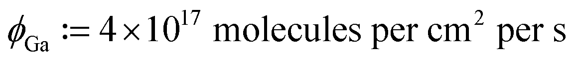 gives close agreement between the simulated via profile, and experiment. Fig. 5(b) shows a surface plot of the simulated Ga+ etched via, with a gas flux ϕGa; note that only 1/4 of the actual line scan is simulated, since we use mirror boundary conditions. Fig. 5(c) compares the derivative of the via depth with respect to dose, and the gas coverage in the bottom of the via; the derivative and gas coverage tend to decrease with increasing dose, however they both exhibit significant noise, likely due to the small variations in gas coverage in this dose range.
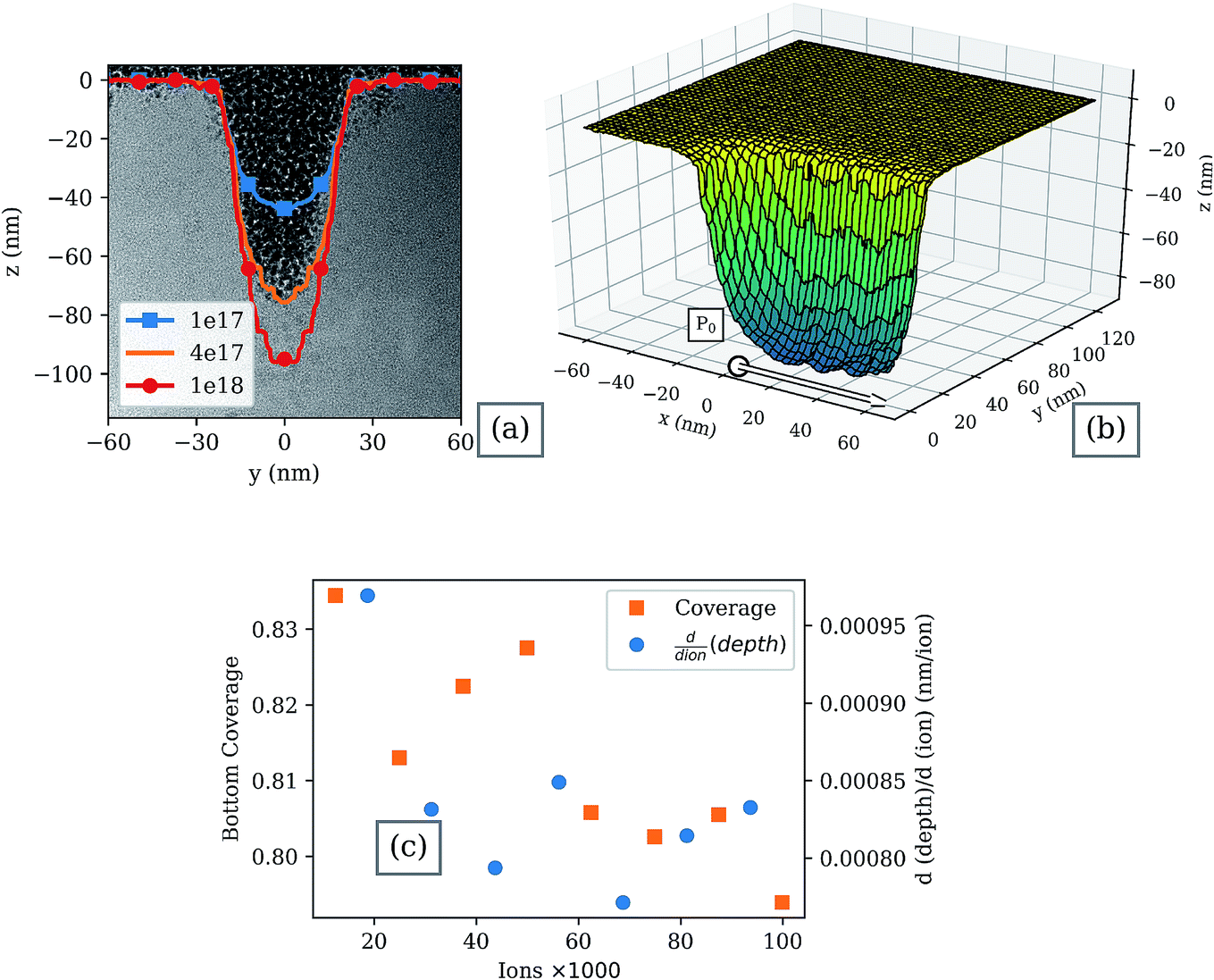 | ||
| Fig. 5 Ga+ etching using the Ga+ effective beam profile, using recipe 5 (in text). (a) Comparison of Ga+ etched vias with experimental TEM image as the gas flux is varied. Gas flux is given in units of molecules per cm2 per s. (b) Surface profile of the etched via with flux 4 × 10¹⁷ molecules per cm2 per s. The entire simulation domain is shown, and there is a mirror boundary condition at the y = 0 plane, and the x = 64 nm plane. The initial position of the beam in the x–y plane is indicated by P0. (c) Comparison of the fractional gas coverage at the via bottom (left axis, square markers) and the absolute value of the change in via depth per ion (right axis, circular markers). The bottom coverage is calculated for surface sites with x ∈ (0, 64) nm and y ∈ (0, 15). | ||
We simulate Ga+ recipes 1–4 using a XeF2 flux of ϕGa; Fig. 6(a) and (b) shows vias resulting from simulations and experiments with a refresh time of 2400 μs, while those in Fig. 6(d)–(f) have a refresh time of 1200 μs. For the purposes of comparison, we plot the simulated via cross-sections with via profiles extracted from the experimental TEM images, shown in Fig. 6 (see ESI† for a comparison between experiments and the actual TEM images). While there is variability in the via depths between the experiments, overall, the experimental etch volumes are reproduced well by simulations. The differences between simulations and experiments are within the variability of the experiments, and the trends in via shape and material removal yield are replicated by the simulations. Additionally, in Fig. 6, we plot the simulated total depth/dose for each recipe. As the dwell time is increased, while the refresh time is held constant, the depth etched per ion decreases; the greatest variability in etch rate is seen between recipes 3 and 5, where the change in depth per ion decreases by a third as the dwell time is increased by a factor of 10. The total removal yields for all Ga+ line scan recipes are summarized in Table 3. Interestingly, the removal rates of Table 3 do not vary as much as the ratio of the etched via depth to ions plotted in Fig. 6(f); this difference can be understood by the fact that the via FWHM varies between recipes, even when etching to the same depth. Ga+via 4, for example, is 15% wider at the same depth as Ga+via 3.
 | ||
| Fig. 6 Comparison of simulated etched via profile (dashed curves) to experimental via profiles (solid curves) for the Ga+ etched via with recipes 1 through 5 ((a), (b), (d)–(f)). The depth/dose plot (c) shows the depth over dose for each recipe, as a function of the dwell time, with the legend corresponding to τrefresh. | ||
| Ga+ 1 | Ga+ 2 | Ga+ 3 | Ga+ 4 | Ga+ 5 | Ne+ 1 | Ne+ 2 | Ne+ 3 | |
| 74.2 | 73.7 | 73.3 | 75.0 | 64.8 | 8.2 | 8.4 | 9.5 |
3.2 Ne+ etching
The results of simulating Ne+ etching recipe 1 of Table 2, are shown in Fig. 7. Again, we treat the effective gas flux as a fitting parameter, and the best agreement with experiments is obtained for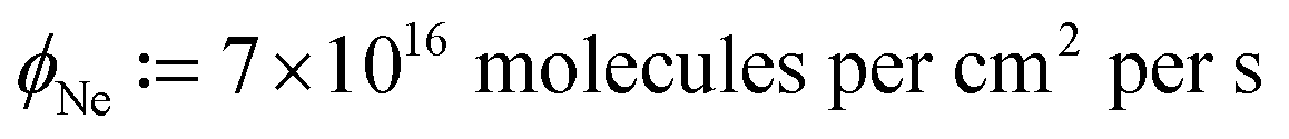 , which is lower than that observed in the Ga+ etching experiments. A plot of the surface of the etched via is also shown in Fig. 7; compared to the Ga+ recipes, the Ne+ etch leads to a deeper and higher aspect ratio via. Note that the Ne+ dose is higher compared to the Ga+ experiments; the lower gas flux, greater via depth, and lower mass of Ne+, lead to a correspondingly lower cumulative etch yield, and sputter yield (6.8 and 0.5 atoms per ion, respectively). The higher aspect ratio via also leads to lower gas coverages, as we would expect from Fig. 2, as shown in Fig. 7(c) on the left axis. Similar to the Ga+ recipes, gas etching is the dominant mechanism by which material is removed from the surface, so the change in via depth with dose is approximately proportional to the coverage of gas in the via bottom, as shown in Fig. 7(c).
 | ||
| Fig. 7 Ne+ etching using the Ne+ Effective Beam Profile, using Ne+ etching recipe 1. (a) Comparison of Ne+ etched vias with experimental SEM image as the gas flux is varied. Gas flux is given in units of molecules per cm2 per s. (b) Surface profile of the etched via with flux 7 × 10¹⁶ molecules per cm2 per s. The entire simulation domain is shown, and there is a mirror boundary condition at the y = 0 plane, and the x = 64 nm plane. The initial position of the beam in the x–y plane is indicated by P0. (c) Comparison of the fractional gas coverage at the via bottom (left axis, square markers) and the absolute value of the change in via depth per ion (right axis, circular markers), for the etching simulation with gas flux 7 × 10¹⁶ molecules per cm2 per s. The bottom coverage is calculated for surface sites with x ∈ (0, 64) nm and y ∈ (0, 15) nm. | ||
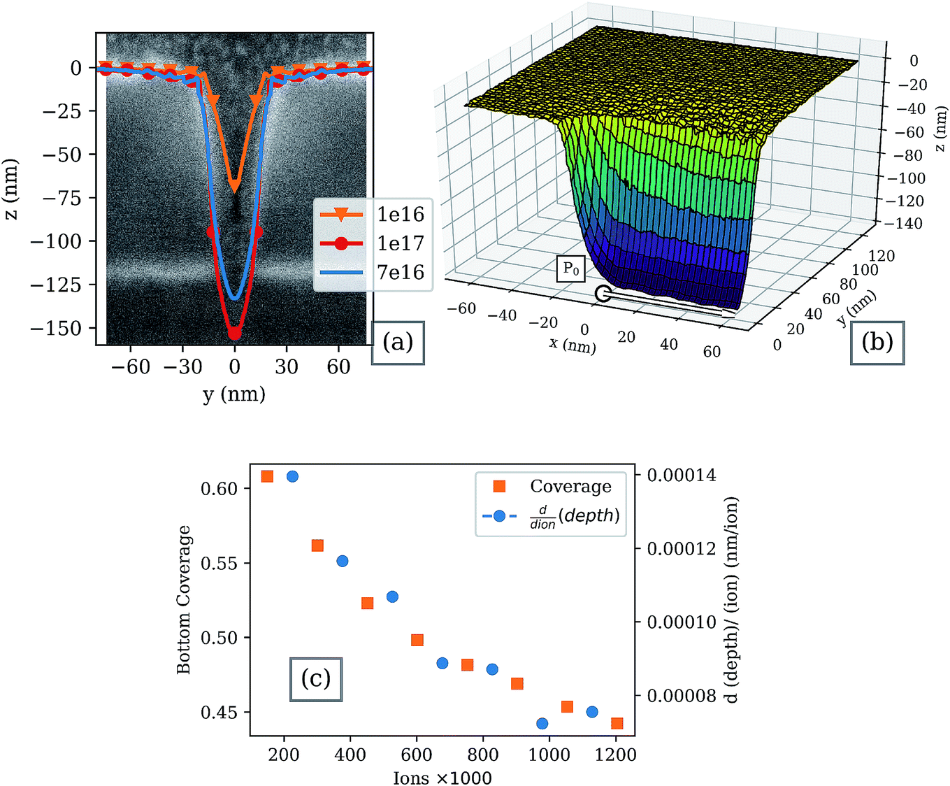
Fig. 8 shows the via profiles resulting from simulations for all Ne+ recipes in Table 2, compared with experimental images. All simulations in Fig. 8 were performed with a gas flux equal to ϕNe. Both the dwell time and refresh time are varied for the Ne+ recipes, however we can see that the overall trend is for the etch rate to increase as the dwell time is reduced: via 3, with a dwell time of 0.2 μs has a 34% higher total removal rate per incident ion, than does via 1, which has a dwell time of 1 μs. When compared to the experimental images, simulations are slightly shallower in recipes 2 and 3. All Ne+ recipes result in vias with a similar FWHM. The material removal rates for all Ne+ recipes are given in Table 3.
 | ||
| Fig. 8 Comparison of simulated etched profile to experimental via profiles for the Ne+ etched via with recipes 1 through 3. | ||
4 Discussion
We consider the relative contributions to via shape formation from sputtering and etching in Fig. 9; here we plot the profile of the simulated etched via using Ne+ recipe 1, with a XeF2 flux of ϕNe, after 121 frames (a), and 1218 frames (b). The shaded regions indicate the cross sections of volume removed by etching, and by sputtering, over this dose range. As expected, etching accounts for the majority of the material removed, and largely determines the via shape. Sputtering is negligible away from the via center, however it contributes a significant fraction of the material removal near the via center. The relative importance of sputtering in the via center can be attributed to lower gas coverage, caused by depletion from the ion beam, and, in deeper vias, a reduced incoming gas flux due to shadowing; this combination of factors reduces the overall etch rate, while the sputter rate is unaffected by gas coverage. Additionally, we see that as a via increases in depth, the via depth is not completely explained by the influence of etching and sputtering, but instead, there is an additional contribution from atoms being sputtered/displaced and redeposited elsewhere in the via (see Fig. 9(b)).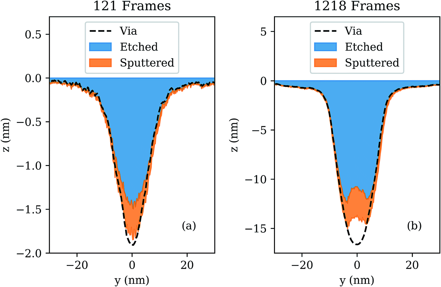 | ||
| Fig. 9 Comparison of the simulated spatial distributions of sputtering and etching for the formation of the Ne+via with recipe 1. The parameters correspond to the first (a) 121 frames, and (b) 1218 frames of the dose. The blue shaded region indicates the cross section of the volume of material removed by etching, and the orange to the volume removed by sputtering. In the shallow via, sputtering is more significant near the beam center, where gas is exhausted, than near the tails where etching dominates. | ||
We compare the beam profile with the associated simulated etched via shape, for both Ga+ recipe 5, and Ne+ recipe 1, in Fig. 10. The Ga+ etched via shows a close similarity between the via shape and the beam shape; however, for the Ne+ etched via, we see that there is a significant difference between the beam and via shapes, with the etched via being wider than the beam profile. This is in contrast to the case for pure sputtering without XeF2, where simulations show that the sputtered via shape is similar to the beam profile for both Ne+ and Ga+ sputtering.29
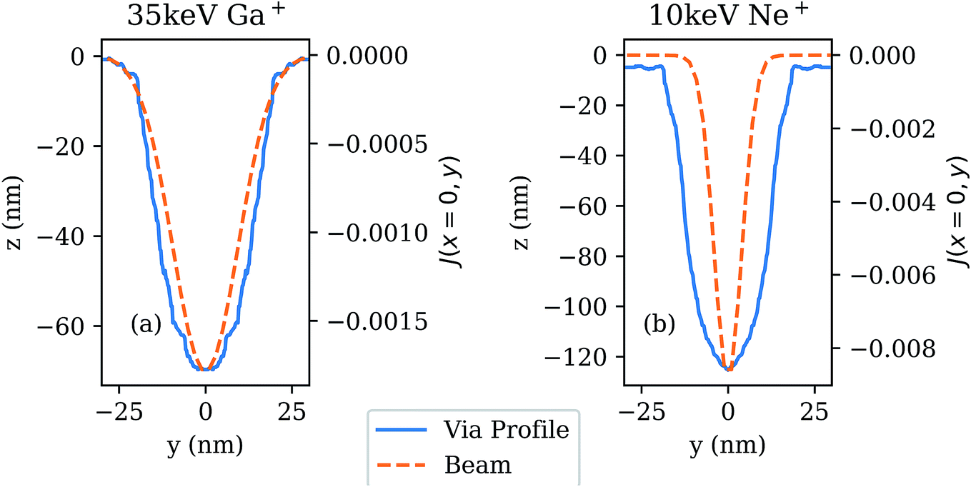 | ||
| Fig. 10 Comparison of the beam shape (dashed lines) and the corresponding etched via profile for the 35 keV Ga+ with recipe 5 with gas flux ϕGa (a), and the 10 keV Ne+ beam with recipe 1 with gas flux ϕNe (b). | ||
To understand why there is such a difference between the beam profile and the via profile for the simulated Ne+ etched via in Fig. 10, we plot the FWHM as a function of via depth for Ne+ recipe 1 with varying gas flux in Fig. 11(a). When the gas flux is 1 × 10¹¹ molecules per cm2 per s, there is near zero chemical etching and the line scan is in a pure sputtering regime. As the gas flux is increased, and etching becomes significant, the FWHM increases as a function of depth, reaching a peak around 1 × 10¹⁶ molecules per cm2 per s, after which it begins to decrease with increased gas flux. When the gas flux reaches a sufficiently high value, the FWHM of the etched via becomes comparable to the pure sputtered via. Importantly, we see that ϕNe falls in the intermediate regime where the FWHM is near maximal as a function of depth. If the flux in the Ne+ etch simulation is increased to 5 × 10¹⁷ molecules per cm2 per s, we see that the etched via profile is narrower, just as in the Ga+ case (see Fig. 11(b)). Therefore, simulations predict that etching resolution is optimal for pure sputtering, or very high gas fluxes. Furthermore, the optimal resolution resulting from XeF2 assisted etching is similar to the effective beam profile, just as in sputtering.29
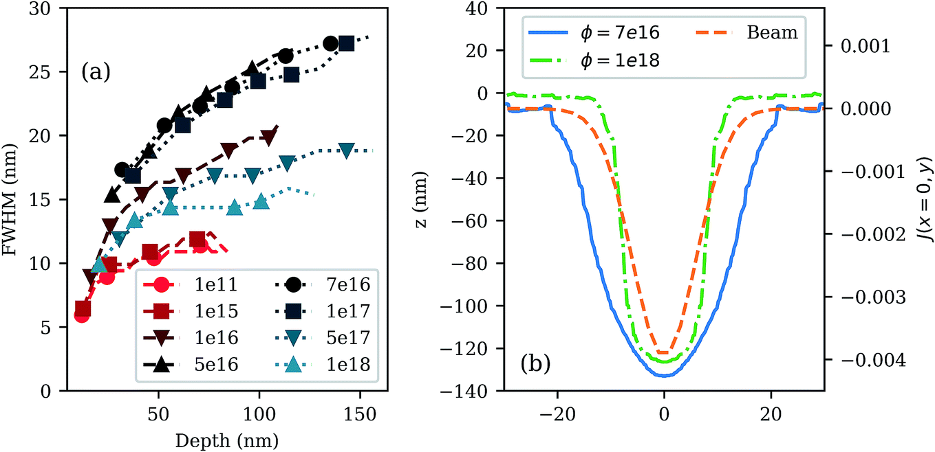 | ||
| Fig. 11 (a) FWHM vs. depth for the Ne+ etched via, with variable gas flux. (b) Comparison of the beam profile, and the Ne+ etched via profile resulting from a gas flux of 7 × 10¹⁶ molecules per cm2 per s at a dose of 20099 frames, and the Ne+ etched profile resulting from a gas flux of 1018 molecules per cm2 per s at a dose of 3343 frames. The legends give the corresponding gas flux in units of molecules per cm2 per s. | ||
5 Conclusion
We present a computational method for simulating gas-assisted ion beam etching; in particular, we study XeF2 assisted FIB induced etching of SiO2. This method is incorporated into the EnvizION simulation, which uses a Monte Carlo simulation of focused ion beam processing. The presented method accounts for an isotropic flux of XeF2 molecules incident on a surface with arbitrary geometry, allowing population of high aspect ratio features such as sputtered valleys. The adsorbed gas can react with the SiO2 molecules due to added energy from the focused ion beam. The etching reactions are dominated by interactions between the recoiling atoms in the target which are displaced by the primary ion; consequently, the etching is driven by energy which is transferred from the primary ion to the substrate by the elastic nuclear energy loss. Diffusion of adsorbed gas molecules is neglected for the present work.We apply the simulation method to study the formation of nanoscale vias with reference to experiments; five recipes are studied for FIB etching using a 35 keV Ga+ beam, and three recipes are studied for FIB etching using a 10 keV Ne+ beam. Effective ion beam profiles are identified for the Ne+ and Ga+ beams, which reproduce the shape of experimental etched vias by combining the innate ion beam profile with possible machining artifacts. Using these beam profiles, we simulate experimental vias using a variable gas flux to identify the experimental gas flux. After identifying the experimental gas flux, the Ga+ and Ne+ etching simulations reproduce experimental vias for all parameter recipes we consider.
Unlike sputtering simulations, the resolution of the simulated etched vias is shown to be strongly dependent on the incoming gas flux. The FWHM of etched vias is found to increase with via depth for the Ne+ etched vias, and the FWHM can vary by as much as a factor of two depending on gas flux. Intermediate gas fluxes are shown to lead to the lowest resolution etching, while pure sputtering, and very high gas flux, produce comparable FWHM as a function of depth.
In a future work, we will analyze the factors determining resolution in detail. In particular, we expect that surface diffusion of adsorbed gas molecules plays a significant role in both the etch rate, and the etching resolution. Additionally, it remains an important open problem to incorporate a simulation of the gas flux, to remove the need for fitting the flux to experimental data.
Conflicts of interest
There are no conflicts to declare.Acknowledgements
The authors acknowledge support from Intel Corporation.References
- J. Morgan, J. Notte, R. Hill and B. Ward, An introduction to the helium ion microscope, Microsc. Today, 2006, 14, 24 CrossRef CAS.
- P. Alkemade, E. Koster, E. van Veldhoven and D. Maas, Imaging and nanofabrication with the helium ion microscope of the van Leeuwenhoek laboratory in delft, Scanning, 2012, 34, 90 CrossRef CAS PubMed.
- D. Fox, Y. B. Zhou, A. O'Neill, S. Kumar, J. Wang, J. Coleman, G. Duesberg, G. Donegan and H. Zhang, Helium ion microscopy of graphene: beam damage, image quality and edge contrast, Nanotechnology, 2013, 24, 335702 CrossRef CAS PubMed.
- H. Wu, L. Stern, J. Chen, M. Huth, C. Schwalb, M. Winhold, F. Porrati, C. Gonzalez, R. Timilsina and P. Rack, Synthesis of nanowires via helium and neon focused ion beam induced deposition with the gas field ion microscope, Nanotechnology, 2013, 24, 175302 CrossRef CAS PubMed.
- H. Wu, L. Stern, D. Xia, D. Ferranti, B. Thompson, K. Klein, C. Gonzalez and P. Rack, Focused helium ion beam deposited low resistivity cobalt metal lines with 10 nm resolution: implications for advanced circuit editing, J. Mater. Sci.: Mater. Electron., 2014, 25, 587 CrossRef CAS.
- P. Alkemade and H. Miro, Focused helium-ion-beam-induced deposition, Appl. Phys. A: Mater. Sci. Process., 2014, 117, 1747 CrossRef.
- R. Livengood, S. Tan, R. Hallstein, J. Notte, S. McVey and F. F. Rahman, The neon gas field ion source - first characterization of neon nanomachining properties, Nucl. Instrum. Methods Phys. Res., Sect. A, 2011, 645(1), 136 CrossRef CAS.
- S. Tan, R. Livengood, Y. Greenzweig, Y. Drezner and D. Shima, Probe current distribution characterization technique for focused ion beam, J. Vac. Sci. Technol., B: Nanotechnol. Microelectron.: Mater., Process., Meas., Phenom., 2012, 30, 06F606 Search PubMed.
- R. Livengood, S. Tan, Y. Greenzweig, J. Notte and S. McVey, Subsurface damage from helium ions as a function of dose, beam energy, and dose rate, J. Vac. Sci. Technol., B: Microelectron. Nanometer Struct.--Process., Meas., Phenom., 2009, 27(6), 3244 CrossRef CAS.
- G. B. Assayag, C. Vieu, J. Gierak, P. Sudraud and A. Corbin, New characterization method of ion current-density profile based on damage distribution of Ga+ focused-ion beam implantation in GaAS, J. Vac. Sci. Technol., B: Microelectron. Nanometer Struct.--Process., Meas., Phenom., 1993, 11(6), 2420–2426 CrossRef.
- S. Jesse, A. Y. Borisevich, J. D. Fowlkes, A. R. Lupini, P. D. Rack, R. R. Unocic, B. G. Sumpter, S. V. Kalinin, A. Belianinov and O. S. Ovchinnikova, Directing matter: toward atomic-scale 3D nanofabrication, ACS Nano, 2016, 10(6), 5600–5618 CrossRef CAS.
- M. G. Stanford, P. R. Pudasaini, A. Belianinov, N. Cross, J. H. Noh, M. R. Koehler, D. G. Mandrus, G. Duscher, A. J. Rondinone and I. N. Ivanov, et al., Focused helium-ion beam irradiation effects on electrical transport properties of few-layer WSe2: enabling nanoscale direct write homo-junctions, Sci. Rep., 2016, 6, 27276 CrossRef CAS PubMed.
- M. G. Stanford, P. R. Pudasaini, E. T. Gallmeier, N. Cross, L. Liang, A. Oyedele, G. Duscher, M. Mahjouri-Samani, K. Wang and K. Xiao, et al., High conduction hopping behavior induced in transition metal dichalcogenides by percolating defect networks: toward atomically thin circuits, Adv. Funct. Mater., 2017, 27(36), 1702829 CrossRef.
- M. G. Stanford, B. B. Lewis, V. Iberi, J. D. Fowlkes, S. Tan, R. Livengood and P. D. Rack, In situ mitigation of subsurface and peripheral focused ion beam damage via simultaneous pulsed laser heating, Small, 2016, 12(13), 1779–1787 CrossRef CAS.
- R. Livengood, Y. Greenzweig, T. Liang and M. Grumski, Helium ion microscope invasiveness and imaging study for semiconductor applications, J. Vac. Sci. Technol., B: Microelectron. Nanometer Struct.--Process., Meas., Phenom., 2007, 25(6), 2547 CrossRef CAS.
- M. G. Stanford, P. R. Pudasaini, N. Cross, K. Mahady, A. N. Hoffman, D. G. Mandrus, G. Duscher, M. F. Chisholm and P. D. Rack, Tungsten diselenide patterning and nanoribbon formation by gas-assisted focused-helium-ion-beam-induced etching, Small, 2017, 1600060 CrossRef.
- K. Ohya, T. Yamanaka, K. Inai and T. Ishitani, Comparison of secondary electron emission in helium ion microscope with gallium ion and electron microscopes, Nucl. Instrum. Methods Phys. Res., Sect. B, 2009, 267(4), 584–589 CrossRef CAS.
- D. A. Smith, D. C. Joy and P. D. Rack, Monte Carlo simulation of focused helium ion beam induced deposition, Nanotechnology, 2010, 21(17), 175302 CrossRef PubMed.
- J. P. Biersack and L. Haggmark, A Monte Carlo computer program for the transport of energetic ions in amorphous targets, Nucl. Instrum. Methods, 1980, 174(1–2), 257–269 CrossRef CAS.
- J. Biersack and L. G. Haggmark, SRIM: The stopping and range of ions in matter, SRIM Co., 2015 Search PubMed.
- W. Möller and W. Eckstein, Tridyn - trim simulation code including dynamic composition changes, Nucl. Instrum. Methods Phys. Res., Sect. B, 1984, 2(1–3), 814 CrossRef.
- W. Boxleitner and G. Hobler, “FIBSIM-dynamic Monte Carlo simulation of compositional and topography changes caused by focused ion beam milling, Nucl. Instrum. Methods Phys. Res., Sect. B, 2001, 180(1), 125 CrossRef CAS.
- W. Boxleitner, G. Hobler, V. Klüppel and H. Cerva, Simulation of topography evolution and damage formation during TEM sample preparation using focused ion beams, Nucl. Instrum. Methods Phys. Res., Sect. B, 2001, 175, 102 CrossRef.
- W. Möller, TRI3DYN-Collisional computer simulation of the dynamic evolution of 3-dimensional nanostructures under ion irradiation, Nucl. Instrum. Methods Phys. Res., Sect. B, 2014, 322, 23 CrossRef.
- R. Timilsina and P. Rack, Monte Carlo simulations of nanoscale focused neon ion beam sputtering, Nanotechnology, 2013, 24, 495303 CrossRef PubMed.
- R. Timilsina, D. Smith and P. Rack, A comparison of neon versus helium ion beam induced deposition via Monte Carlo simulations, Nanotechnology, 2013, 24, 175302 CrossRef PubMed.
- R. Timilsina, S. Tan, R. Livengood and P. Rack, Monte Carlo simulations of nanoscale focused neon ion beam sputtering of copper: elucidating resolution limits and sub-surface damage, Nanotechnology, 2014, 25, 485704 CrossRef CAS PubMed.
- K. Mahady, S. Tan, Y. Greenzweig, R. Livengood, A. Raveh and P. D. Rack, Monte Carlo simulations of nanoscale Ne+ ion beam sputtering: investigating the influence of surface effects, interstitial formation, and the nanostructural evolution, Nanotechnology, 2016, 28(4), 045305 CrossRef PubMed.
- K. T. Mahady, S. Tan, Y. Greenzweig, A. Raveh and P. D. Rack, Simulating advanced focused ion beam nanomachining: a quantitative comparison of simulation and experimental results, Nanotechnology, 2018, 29(49), 495301 CrossRef.
- K. Mahady, S. Tan, Y. Greenzweig, R. Livengood, A. Raveh, J. D. Fowlkes and P. D. Rack, Monte Carlo simulations of secondary electron emission due to ion beam milling, J. Vac. Sci. Technol., B: Nanotechnol. Microelectron.: Mater., Process., Meas., Phenom., 2017, 35(4), 041805 Search PubMed.
- M. G. Stanford, K. Mahady, B. B. Lewis, J. D. Fowlkes, S. Tan, R. Livengood, G. A. Magel, T. M. Moore and P. D. Rack, Laser-assisted focused He+ ion beam induced etching with and without XeF2 gas assist, ACS Appl. Mater. Interfaces, 2016, 8(42), 29155 CrossRef CAS PubMed.
- A. D. Dubner, Mechanism of ion beam induced deposition, PhD thesis, Massachusetts Institute of Technology, 1990.
- A. Dubner, A. Wagner, J. Melngailis and C. Thompson, The role of the ion-solid interaction in ion-beam-induced deposition of gold, J. Appl. Phys., 1991, 70(2), 665–673 CrossRef CAS.
- H.-J. Fitting and J.-U. Friemann, Monte-Carlo studies of the electron mobility in SiO2, Phys. Status Solidi A, 1982, 69(1), 349 CrossRef CAS.
- L. R. Harriott, Digital scan model for focused ion beam induced gas etching, J. Vac. Sci. Technol., B: Microelectron. Nanometer Struct.--Process., Meas., Phenom., 1993, 11(6), 2012 CrossRef CAS.
- D. Smith, J. Fowlkes and P. Rack, A nanoscale three-dimensional Monte Carlo simulation of electron-beam-induced deposition with gas dynamics, Nanotechnology, 2007, 18, 265308 CrossRef CAS PubMed.
- W. Van Dorp, J. Wnuk, J. Gorham, D. Fairbrother, T. Madey and C. Hagen, Electron induced dissociation of trimethyl (methylcyclopentadienyl) platinum(IV): total cross section as a function of incident electron energy, J. Appl. Phys., 2009, 106(7), 074903 CrossRef.
- R. M. Thorman, T. Ragesh Kumar, D. H. Fairbrother and O. Ingólfsson, The role of low-energy electrons in focused electron beam induced deposition: four case studies of representative precursors, Beilstein J. Nanotechnol., 2015, 6, 1904 CrossRef CAS PubMed.
- M. Toth, C. J. Lobo, G. Hartigan and W. Ralph Knowles, Electron flux controlled switching between electron beam induced etching and deposition, J. Appl. Phys., 2007, 101(5), 054309 CrossRef.
- M. G. Lassiter and P. D. Rack, Nanoscale electron beam induced etching: a continuum model that correlates the etch profile to the experimental parameters, Nanotechnology, 2008, 19(45), 455306 CrossRef PubMed.
- D. A. Smith, J. D. Fowlkes and P. D. Rack, Simulating the effects of surface diffusion on electron beam induced deposition via a three-dimensional Monte Carlo simulation, Nanotechnology, 2008, 19(41), 415704 CrossRef PubMed.
- J. D. Fowlkes and P. D. Rack, Fundamental electron-precursor-solid interactions derived from time-dependent electron-beam-induced deposition simulations and experiments, ACS Nano, 2010, 4(3), 1619–1629 CrossRef CAS PubMed.
Footnote |
| † Electronic supplementary information (ESI) available. See DOI: 10.1039/c9na00390h |
| This journal is © The Royal Society of Chemistry 2019 |