
 Open Access Article
 This Open Access Article is licensed under a Creative Commons Attribution-Non Commercial 3.0 Unported Licence
Enhanced thermoelectric properties of lightly Nb doped SrTiO3 thin films†
S.
Bhansali
a,
W.
Khunsin
a,
A.
Chatterjee
a,
J.
Santiso
 a,
B.
Abad
b,
M.
Martin-Gonzalez
b,
G.
Jakob
cd,
C. M.
Sotomayor Torres
ae and
E.
Chávez-Angel
*a
a,
B.
Abad
b,
M.
Martin-Gonzalez
b,
G.
Jakob
cd,
C. M.
Sotomayor Torres
ae and
E.
Chávez-Angel
*a
aCatalan Institute of Nanoscience and Nanotechnology (ICN2), CSIC, The Barcelona Institute of Science and Technology, Campus UAB, Bellaterra, 08193 Barcelona, Spain. E-mail: emigdio.chavez@icn2.cat
bInstituto de Microelectronica de Madrid, IMM-CNM, CSIC, Isaac Newton, 8 PTM, 28760 Tres Cantos (Madrid), Spain
cInstitut für Physik, Johannes Gutenberg Universität Mainz, Staudingerweg 7, 55128 Mainz, Germany
dGraduate School Materials Science in Mainz, Staudingerweg 9, 55128 Mainz, Germany
eICREA, Passeig Lluis Companys 23, 08010 Barcelona, Spain
First published on 7th August 2019
Abstract
Novel thermoelectric materials developed for operation at room temperature must have similar or better performance along with being as ecofriendly as those commercially used, e.g., Bi2Te3, in terms of their toxicity and cost. In this work, we present an in-depth study of the thermoelectric properties of epitaxial Nb-doped strontium titanate (SrTi1−xNbxO3) thin films as a function of (i) doping concentration, (ii) film thickness and (iii) substrate type. The excellent crystal quality was confirmed by high resolution transmission electron microscopy and X-ray diffraction analysis. The thermoelectric properties were measured by the three-omega method (thermal conductivity) and van der Pauw method (electrical resistivity), complemented by Seebeck coefficient measurements. A maximum power factor of 8.9 × 10⁻³ W m−1 K−2 and a thermoelectric figure of merit of 0.49 were measured at room temperature in 50 nm-thick films grown on lanthanum strontium aluminate. The mechanisms behind this high figure of merit are discussed in terms of a possible two-dimensional electron gas, increase of the effective mass of the electrons, electron filtering and change in strain due to different substrates. The overall enhancement of the thermoelectric properties suggests that SrTi1−xNbxO3 is a very promising n-type candidate for room- to high-temperature applications.
Introduction
Alkaline earth metal titanates ATiO3 (A = Ba, Sr, or Ca) with a perovskite structure are materials of fundamental and technological importance due to a broad range of industrial applications1–4 and more recently because of their thermoelectric potential.5–8 Although the stoichiometric A2+Ti4+O3 is a band insulator with an energy gap of ∼2–3.3 eV,9 tuning the chemical composition allows for the injection of carriers (electrons) into the conduction band, composed mainly of Ti 3d t2g orbitals. Doping with aliovalent cation substituents has been extensively examined, for example, using trivalent cations (e.g., La3+) at the A site10,11 or pentavalent cations (e.g., Nb5+ and Sb5+) at the Ti site.12,13 Oxygen deficient perovskite ATiO3−δ has also been investigated.14,15 Strontium titanate (SrTiO3, STO) thin films and superlattices have been studied for various applications using lanthanum strontium aluminate ((LaAlO3)0.3–(Sr2AlTaO6)0.7, LSAT) as a substrate.16,17 Room-temperature ferroelectricity has been demonstrated by growing STO with in-plane tensile strain on DyScO3 (DSO).18 In this respect, STO is also becoming a material of choice among oxide thermoelectrics, as the carrier concentration and Seebeck coefficients become increasingly promising.17,19,20 In a thermoelectric material, three important parameters have to be considered, namely the Seebeck coefficient (S), electrical conductivity (σ) and thermal conductivity (k). From these parameters, the dimensionless figure of merit ZT = S2σT/k can be defined, where T is the mean working temperature. For industrial applications and competitive energy conversion ZT ≥ 1 is considered to be a desirable benchmark.21,22 Figures of ZT > 1 have already been reported for p-type oxides;23,24 however, for n-type oxides, ZT barely exceeds 0.5,25 and this value has only been measured in ZnO ceramics at very high temperatures (T > 1000 K).26 For STO-based materials, the highest experimental ZT reported to date is 0.46 at T = 1000 K, which was measured in a Pr (5%):Nb (20%)-doped STO superlattice.27 Theoretical predictions also estimate values as high as 0.7 in La doped SrTiO3.28 In this context, more investigation is needed to engineer thermoelectric properties in n-type oxides for higher ZT.29,30In this work we report on the enhancement of the thermoelectric properties of STO thin films with low Nb-doping content. An in-depth study of the thermoelectric properties of these films was carried out considering the (i) doping concentration, (ii) film thickness and (iii) type of substrate. Based on these three parameters, this work has been divided into three sections as follows:
(i) Doping analysis: the first step consisted of investigating the impact of doping content on the thermoelectric properties. Fixing the type of substrate (lanthanum aluminate, LAO) and the film thickness (50 nm), the Nb-content was varied from 2 to 5 and 15% mol. Once the optimum Nb-content with the highest thermopower value was found (2% mol), we proceeded with the thickness study.
(ii) Thickness analysis: the second step consisted of fixing the substrate and doping concentration and varying the film thickness. Seven films with thicknesses of 30, 50, 66, 99, 160, 165 and 200 nm were grown on an LAO substrate. Finally, with the optimum doping concentration (2% mol) and film thickness (50 nm), the study of the impact of the type of substrate on the thermoelectric properties was carried out.
(iii) Substrate analysis: in this last step, four different substrates were used, namely, LSAT, DSO, LAO and LaSrAlO4 (LSAO). Together with the thermoelectric properties, the crystallographic features of the grown films were discussed and compared. Our findings show that stress plays an important role in the measured thermoelectric properties. We observed that the films with low stress presented the largest thermoelectric figure of merit. It is important to note that despite being structurally compatible with strontium titanate, LSAT, DSO and LSAO substrates have so far not been well studied. In fact, surprisingly little is known about the thermoelectric properties of STO thin films on these substrates and the interface between them, despite their potentially important role in determining the overall electronic structure of the system.
The combination of these steps allows us to find the optimum configuration of Nb-content, film thickness and substrate type with the largest thermoelectric figure of merit.
(i) Doping analysis: impact of the doping concentration on the power factor for a 50 nm NB:STO film on an LAO substrate
In this section, we study the impact of the doping concentration on the thermoelectric properties of Nb-doped STO thin films. Fixing the type of substrate and the film thickness (50 nm), we grew three films with different amounts of Nb (2%, 5% and 15% mol). The films were characterized by scanning electron microscopy (SEM) and X-ray diffraction (XRD). Fig. 1a displays the XRD patterns of 50 nm-thick films grown on an LAO substrate with 2, 5 and 15 mol% Nb-doped STO showing all (00i) planes of the STO structure. The Nb-doped STO (NB:STO) thin film samples exhibit high crystal quality with a perovskite structure. The elemental composition and oxidation states of the Nb:STO films were analyzed by XPS and the results are shown in Fig. S1 in the ESI.† | ||
| Fig. 1 (a) XRD crystallographic planes of the doped Nb:STO films with different Nb contents deposited on LaAlO3 (LAO). Scanning electron microscopy (b) and high-resolution transmission electron microscopy (c) images of the epitaxial growth of Nb doped SrTiO3 thin film on the LaAlO3 substrate. | ||
The temperature dependence of the Seebeck coefficient of the Nb:STO films is shown in Fig. 2a. The Seebeck coefficient is found to decrease with increasing doping content.33 This is expected as S ∝ (n)−2/3, where n is the carrier concentration,5 and these results are consistent with those reported in the literature.34 It is worth mentioning that the conductive state in the 2% Nb-doped film is barely metallic, i.e., it has a low Fermi energy. The Seebeck coefficient is expected to rise due to a large entropy term arising from the six-fold degeneracy of the Ti 3d t2g conduction bands, since in these thin films the bottom of the conduction band is predominantly formed by Ti 3d orbitals.35 As the 2%-doped film showed the highest power factor (S2σ) (see Fig. 2b), the selected doping for the rest of this work was chosen to be 2 mol%.
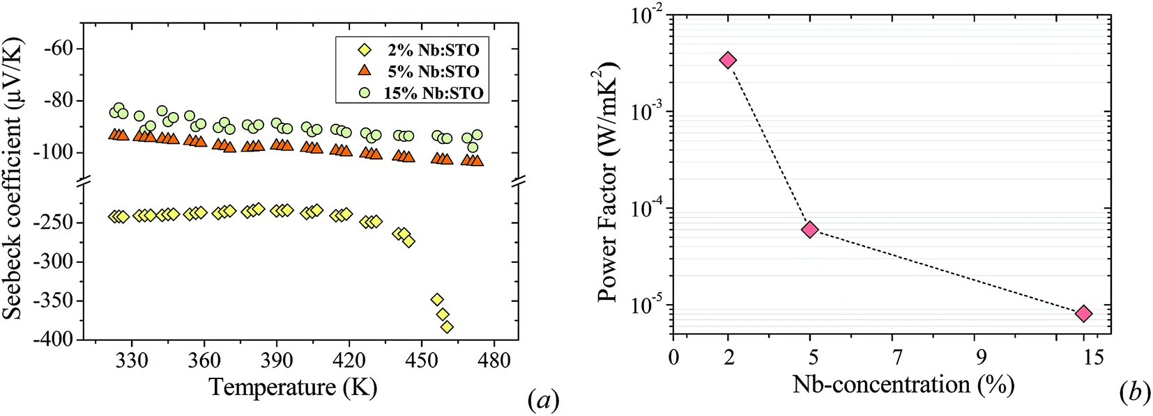 | ||
| Fig. 2 (a) Seebeck coefficient as a function of temperature. (b) Power factor of 2, 5 and 15 mol% 50 nm-thick Nb-doped STO on LAO at room temperature. | ||
Fig. 1b and c display images of a 2 mol% Nb:STO thin film from scanning electron microscopy (SEM) and high-resolution transmission electron microscopy (HRTEM), respectively. The SEM image of the Nb:STO thin film shows the homogeneity of the film on the substrate. The HRTEM image again confirms the epitaxial growth of Nb:STO on the LAO substrate in the 001 direction. Due to the growth steps followed, electron microscopy suggests that the sharp interfaces and homogeneous films may reduce interface scattering of electrons, enhance carrier mobility, and hence increase the electrical conductivity31,32 as we will discuss later.
(ii) Thickness analysis: study of thermoelectric properties vs. film thickness on the LAO substrate
In this section, we study the role of the film thickness in determining the thermoelectric properties of the films. Fixing the type of substrate (LAO) and the doping concentration with the largest thermopower (2% mol), we grew seven films with thickness varying from 30 to 200 nm. Fig. 3a and b show the dependence of the Seebeck coefficient and carrier concentration on the film thickness. By plotting these with respect to each other, i.e. S vs. n, for each film thickness we can observe a strong deviation from the Pisarenko plot (Fig. 3c). This can be associated with the presence of a two-dimensional electron gas (2DEG) as has been demonstrated by Ohta et al.36 and/or a thickness dependence of the effective mass. The dependence of the Seebeck coefficient on the carrier concentration is described by the Pisarenko formula as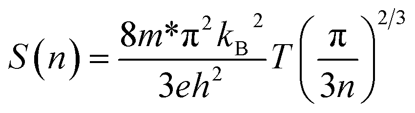 | (1) |
 | ||
| Fig. 3 Thermoelectric properties of 2% Nb-doped STO films grown on the LAO substrate measured at room temperature: (a) Seebeck coefficient and (b) charge carrier concentration as a function of thickness. (c) Seebeck coefficient as a function of charge carrier concentration in comparison to the Pisarenko plot. (d) Power factor as a function of thickness. | ||
Enhanced power factor values in the range of 0.75–3.40 × 10⁻³ W m−1 K−2 were obtained with the measured Seebeck coefficient and electrical conductivity (Fig. 3d). These values are higher than those previously reported in the literature for Nb-substituted bulk STO (0.1 to 1 × 10⁻³ W m−1 K−2).41
The temperature dependence of the Seebeck coefficient and the power factor for the different thicknesses can be found in the ESI.†
(iii) Substrate analysis: thermoelectric properties as a function of different substrates
Once we have narrowed down the optimum film thickness and Nb content showing the highest power factor, we focused on the impact of the substrate and the strain produced by it on the thermoelectric properties of the films. Fixing the film thickness (50 nm) and the Nb-doping concentration (2% mol), epitaxial thin films were grown on LSAT, SLAO and DSO. Here, we focus on the impact of the strain and the interface termination on the film properties. The epitaxial strain is induced in the film due to lattice mismatch with the substrate (see Table 1). The choice of different substrates serves as an important parameter to control the strain in the films. It has been shown that a change in strain can be responsible for the enhancement of the physical properties including the electronic structure, electrical conductivity and ionic diffusion.42–46| Substrate | Lattice parameter, as (Å) | Lattice mismatchaε = (as – a0)/a0 × 100 | Power factor (10−3 W m−1 K−2) | ZT |
|---|---|---|---|---|
| a a 0 is the unstrained lattice parameter of the film. | ||||
| LAO (100) | 3.821 | −2.02 | 3.40 | 0.18 |
| LSAT (100) | 3.868 | −0.82 | 8.91 | 0.49 |
| LSAO (100) | 3.750 | −3.84 | 0.37 | 0.02 |
| DSO (110), pseudo cubic | 3.940 | 1.10 | 0.87 | 0.04 |
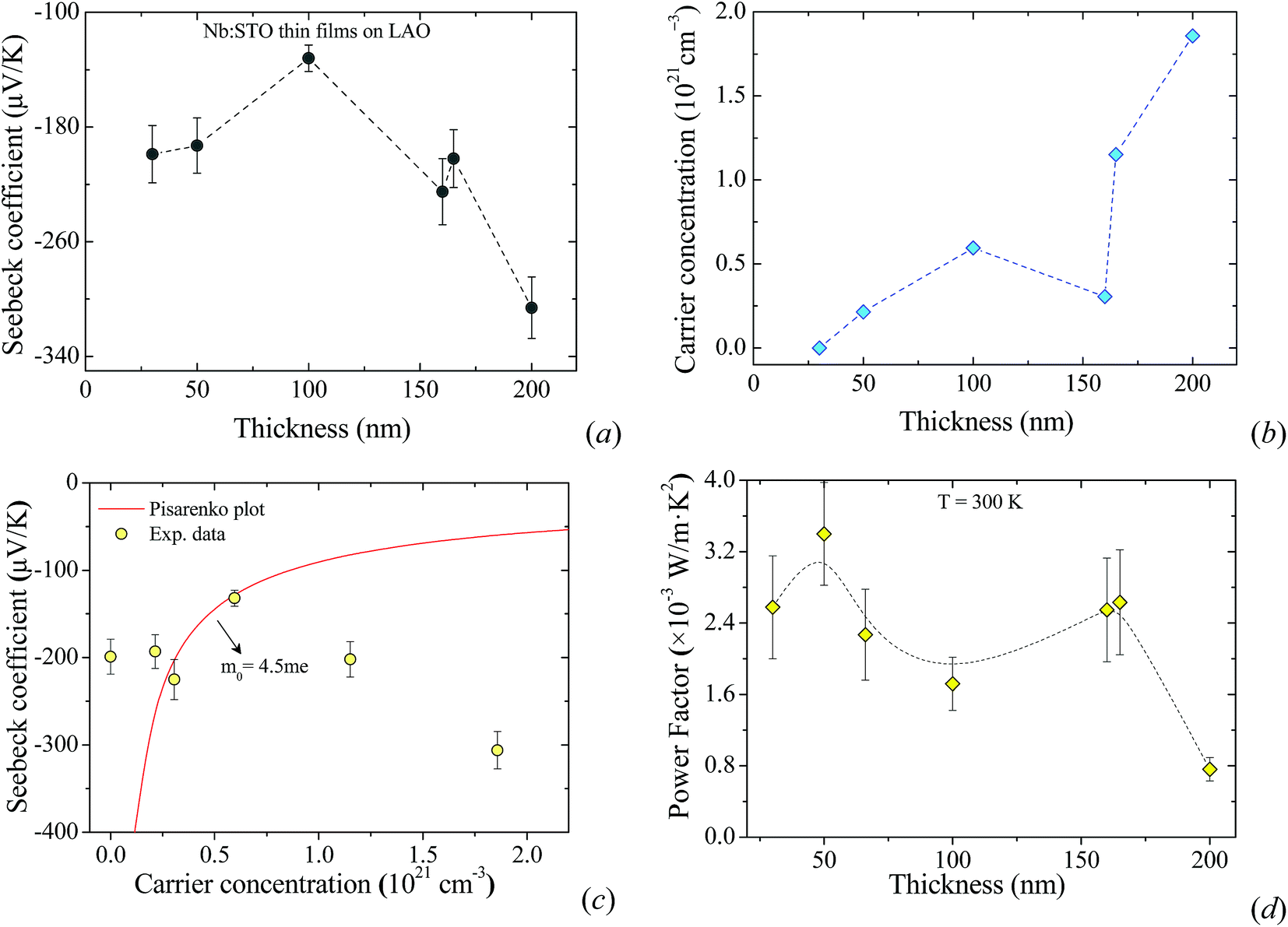
The thermoelectric properties were measured for various substrates as shown in Fig. 4, as Nb:STO films on these substrates are significantly less studied than on LAO. The absolute Seebeck coefficient and power factor on these substrates were estimated to be in the range of 153–321 μV K−1 and 0.3–8.9 × 10⁻³ W m−1 K−2, respectively. As can be seen in Fig. 4, LSAT proved to be the best substrate for the epitaxial growth of Nb:STO thin film. LSAT gave the highest Seebeck coefficient (−320 μV K−1) and power factor (8.9 × 10⁻³ W m−1 K−2). This can be attributed firstly to the reconstruction of the SrO terminated surfaces of these films on the LSAT or LAO substrate due to stress.47 It is very important for the surface and the interface of the film and the substrate to be smooth for better mobility and electrical properties of the system.
 | ||
| Fig. 4 (a) Seebeck coefficient as a function of temperature of Nb:STO thin films on several substrates. (b) Power factor and thermoelectric figure of merit of Nb:STO film on the studied substrates at room temperature. | ||
In many of these systems, the high Seebeck coefficient can also be attributed to a 2DEG, though whether any free electrons might diffuse into the LSAT substrate is currently unknown. In the literature, the opposite scenario has been investigated, i.e., LSAT films grown on STO, and has also yielded evidence of 2DEG formation at the interface, attributed to the polar discontinuity between the mixed polarity of LSAT and non-polar STO.48 Huang et al.47 postulated a mixture of localized holes and a 2DEG within the STO substrate as a result of the mixed polarity of LSAT, which is claimed to have regions of LaAlO3- and Sr2AlTaO6-like character.
Fig. 5a shows the XRD pattern of a 55 nm-thick film grown on an LSAT substrate showing all (00i) planes of the STO structure. In addition, the crystal and epitaxial quality can also be observed in the sharp rocking curve of the (002) peak of the sample grown on LSAT compared to LAO (see Fig. 5b). The rocking curves reveal the broadening of a given diffraction peak. Then, defects such as mosaicity, atomic intermixing, and dislocations, among others lead to the spreading of crystal planes and thus a broadening of the linewidth.49 The sharp rocking curve of the (002) peak observed in Nb:STO/LSAT can be mainly attributed to the extremely good epitaxial quality of the film as can be seen in the reciprocal space map (see Fig. 5c) and in the HRTEM image (see Fig. 5d).
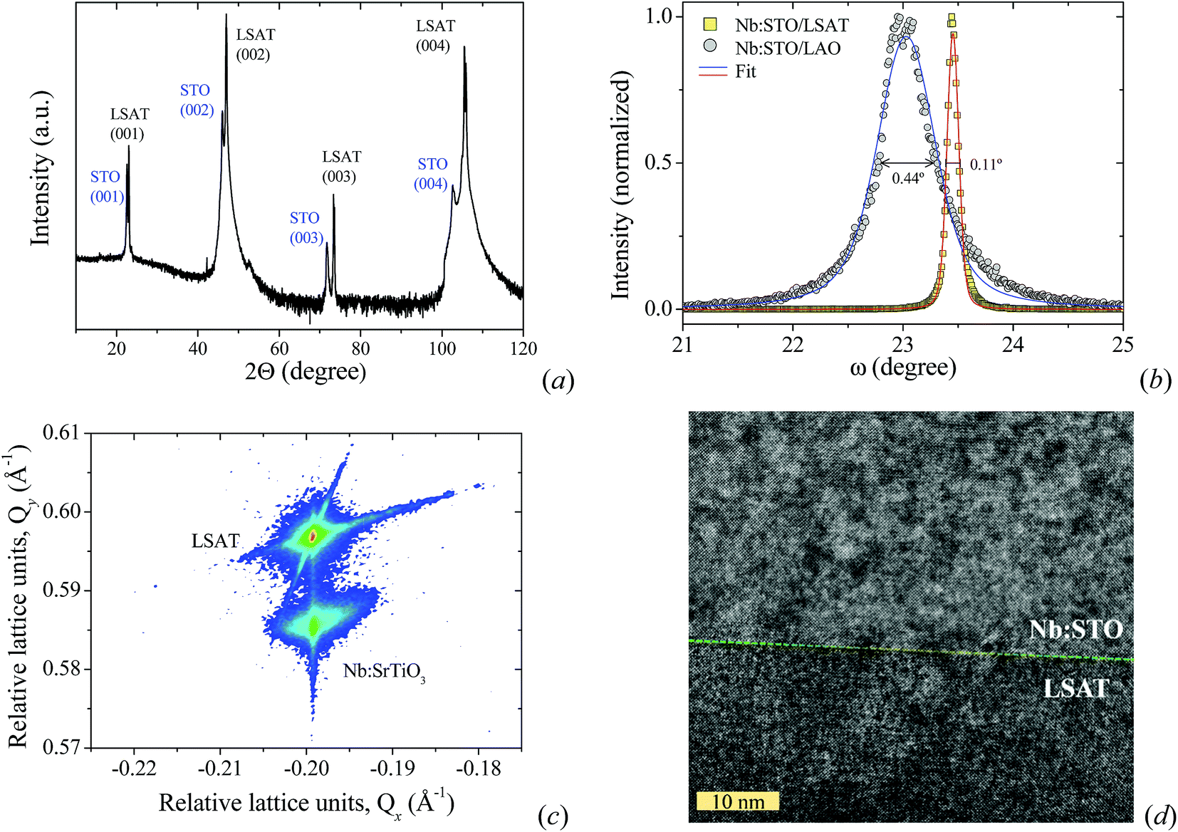 | ||
| Fig. 5 (a) XRD pattern of a 55 nm-thick film of 2%-doped Nb:STO on an LSAT substrate. (b) Rocking curve of the (002) peak of 55 and 50 nm-thick 2%-doped Nb:STO grown on LSAT (yellow squares) and LAO substrates (grey circles), respectively. (c) Reciprocal space map and (d) HRTEM image of 55 nm-thick 2%-Nb doped SrTiO3 film grown on an LSAT substrate. | ||
The thermopower of samples on a DSO substrate also shows very promising values compared to that on the SLAO substrate. This may be due to its smaller mismatch between the lattice parameters, which is compensated for by the elastic strain of the layer and its elasticity-mediated interaction with the upper face of the substrate.50,51
Finally, we estimated the thermoelectric figure of merit using the thermal conductivity measured by the 3ω-method52,53 in the differential configuration.54,55 In this method, the temperature rise of two similar thin film samples of different thicknesses is compared. The thinnest sample acts as a reference while the thickest one will be the film under study. In our case, two Nb:STO thin films with thicknesses of 10 nm and 60 nm were grown on MgO substrates. MgO substrates were chosen because, at room temperature, MgO has a thermal conductivity value of k = 50 W m−1 K−1, while the other substrates have k of the order of 4–12 W m−1 K−1.56 Therefore, the use of MgO as a substrate avoids the two-dimensional spreading of the heat supplied by the 3ω-heater into the thin film, and the k of the films can be obtained using the difference of the temperature rise (see Fig. S4b in the ESI†). An extended and detailed explanation of this methodology can be found in the ESI of ref. 57. Table 1 summarizes the measured power factor and the thermoelectric figure of merit estimated from the experimental thermal conductivity of a 50 nm-thick Nb:STO film: k = 5.44 ± 1.0 W K−1 m−1. By assuming that the thermal conductivity does not change very much with respect to the different substrates, the highest thermoelectric figure of merit was estimated to be ZT = 0.49 for samples grown on LSAT substrates at room temperature.
Summary
In summary, a series of epitaxial and monocrystalline Nb-doped SrTiO3 thin films were grown by PLD on different substrates. From our set of samples (2, 5, and 15% mol Nb:STO), we observed that a doping level of 2% of Nb yielded the maximum power factor for a 50 nm-thick epitaxial film grown on an LaAlO3 substrate. By keeping this doping concentration fixed and varying the film thickness, we found an optimum film thickness of 50 nm on the same substrate with a maximum power factor at room temperature of PF = 3.40 × 10⁻³ W m−1 K−2. After narrowing the doping concentration and the film thickness, we studied the impact of the substrate on the thermoelectric properties. We found that samples grown on lanthanum strontium aluminate ((LaAlO3)0.3–(Sr2AlTaO6)0.7 or LSAT) provided the highest power factor of PF = 8.91 × 10⁻³ W m−1 K−2. Finally, the thermoelectric figure of merit was estimated using the experimental thermal conductivity of Nb:STO films grown on MgO and the measured power factor for each thin film. Outstanding ZT was achieved for films grown on LSAT and LAO substrates with values as high as ZT = 0.49 and 0.18 at room temperature. LSAT was found to be the most convenient substrate with a very high power factor, yielding improved ZT values at room temperature.Methodology
The thin films were deposited using an STO target with different amounts of Nb (2, 5 and 15 mol%). All targets were characterized by using XRD as shown in Fig. S3 in the ESI.† The powder XRD patterns are comparable to that of pure STO (JCPDS card no. 73-0661). An extended description of the target preparation can be found in the ESI.† The deposition rate was fixed at 1 pulse per s with systematic toggling and rotation at 15 rpm at high temperature (T = 1200 K) and low pressure (p = 10−2 to 10−3 mTorr).The film thicknesses were measured by X-ray reflectivity (XRR), up to 100 nm. Thicker samples were measured by ellipsometry (Semilab GES5E) with a rotating analyzer over angles of incidence from 55 to 75° in steps of 5° from 1.22 to 5.53 eV. The in-plane and out-of-plane lattice parameters were obtained from reciprocal space maps of the (−103) reflection obtained from X-ray diffraction (XRD). The XRD spectra were measured using a Malvern-Panalytical X'pert Pro MRD (multipurpose X-ray diffractometer) tuned to Cu K-alpha radiation of wavelength 1.54598 Å. The atomic composition was determined by X-ray photoelectron spectroscopy (XPS) at a base pressure of 1 × 10⁻¹⁰ mbar using monochromatic Al Kα radiation (1486.74 eV) as an excitation source. The surfaces of the films were characterized using atomic force microscopy (AFM) and the surface roughness was found to be <1 nm. The AFM images can be found in the ESI.† Hall measurements were made in 5 × 5 mm2 square-shaped samples in the van der Pauw geometry with ohmic contacts of Cr/Au (5 nm/200 nm) deposited by electron beam evaporation. The Seebeck coefficient was measured in samples of 10 × 5 mm2 using a Linseis LSR setup, ensuring that, for each temperature gradient, sufficient time elapsed to stabilize the temperature and voltage differences. Finally, the thermal conductivity of the 50 nm-thick Nb-doped SrTiO3 thin film was estimated using the three-omega (3ω) method52,53 in the differential configuration.54,55
Conflicts of interest
There are not conflicts to declare.Acknowledgements
The Catalan Institute of Nanoscience and Nanotechnology (ICN2) acknowledges support from the Severo Ochoa Program (MINECO, Grant SEV-2017-0706) and funding from the CERCA Programme/Generalitat de Catalunya. Funding from the Spanish Ministry MINECO/FEDER: FIS2015-70862-P PHENTOM is also acknowledged. AC and JS acknowledge support from the projects MINECO ref. MAT2016-77100-C2-1-P and CNRS-CSIC PICS Project ref. 261091, the EU for funding through project H2020-MSCA-RISE-2014 ref. 645658, and the AGAUR agency for support through project 2017SGR.References
- D. Kan, T. Terashima, R. Kanda, A. Masuno, K. Tanaka, S. Chu, H. Kan, A. Ishizumi, Y. Kanemitsu, Y. Shimakawa and M. Takano, Nat. Mater., 2005, 4, 816–819 CrossRef CAS.
- Properties and Applications of Perovskite-Type Oxides, ed. L. Tejuca and J. Fierro, CRC Press, Boca Raton, 1992 Search PubMed.
- J. H. Haeni, P. Irvin, W. Chang, R. Uecker, P. Reiche, Y. L. Li, S. Choudhury, W. Tian, M. E. Hawley, B. Craigo, A. K. Tagantsev, X. Q. Pan, S. K. Streiffer, L. Q. Chen, S. W. Kirchoefer, J. Levy and D. G. Schlom, Nature, 2004, 430, 758–761 CrossRef CAS PubMed.
- J. J. Choi and S. J. L. Billinge, Nanoscale, 2016, 8, 6206–6208 RSC.
- G. J. Snyder and E. S. Toberer, Nat. Mater., 2008, 7, 105–114 CrossRef CAS PubMed.
- H. Wang, W. Su, J. Liu and C. Wang, J. Materiomics, 2016, 2, 225–236 CrossRef.
- T. Ye, X. Wang, X. Li, A. Q. Yan, S. Ramakrishna and J. Xu, J. Mater. Chem. C, 2017, 5, 1255–1260 RSC.
- T. Wu and P. Gao, Materials, 2018, 11, 999 CrossRef PubMed.
- P. Kanhere and Z. Chen, Molecules, 2014, 19, 19995–20022 CrossRef PubMed.
- P. Pichanusakorn and P. Bandaru, Mater. Sci. Eng., R, 2010, 67, 19–63 CrossRef.
- F. Aguesse, A.-K. Axelsson, P. Reinhard, V. Tileli, J. L. M. Rupp and N. M. Alford, Thin Solid Films, 2013, 539, 384–390 CrossRef CAS.
- W. Wunderlich, S. Ohta, H. Ohta and K. Koumoto, in ICT 2005. 24th International Conference on Thermoelectrics, 2005, IEEE, 2005, pp. 252–255 Search PubMed.
- B. Zhang, J. Wang, T. Zou, S. Zhang, X. Yaer, N. Ding, C. Liu, L. Miao, Y. Li and Y. Wu, J. Mater. Chem. C, 2015, 3, 11406–11411 RSC.
- D. L. Medlin and G. J. Snyder, Curr. Opin. Colloid Interface Sci., 2009, 14, 226–235 CrossRef CAS.
- M. S. Dresselhaus, G. Chen, M. Y. Tang, R. G. Yang, H. Lee, D. Z. Wang, Z. F. Ren, J.-P. Fleurial and P. Gogna, Adv. Mater., 2007, 19, 1043–1053 CrossRef CAS.
- F. Sánchez, C. Ocal and J. Fontcuberta, Chem. Soc. Rev., 2014, 43, 2272–2285 RSC.
- Y.-Y. Pai, A. Tylan-Tyler, P. Irvin and J. Levy, Rep. Prog. Phys., 2018, 81, 36503 CrossRef PubMed.
- S. R. S. Kumar, A. Z. Barasheed and H. N. Alshareef, ACS Appl. Mater. Interfaces, 2013, 5, 7268–7273 CrossRef CAS PubMed.
- S. Ohta, T. Nomura, H. Ohta and K. Koumoto, J. Appl. Phys., 2005, 97, 34106 CrossRef.
- H. Ohta, S. Kim, Y. Mune, T. Mizoguchi, K. Nomura, S. Ohta, T. Nomura, Y. Nakanishi, Y. Ikuhara, M. Hirano, H. Hosono and K. Koumoto, Nat. Mater., 2007, 6, 129–134 CrossRef CAS PubMed.
- H. Goldsmid, Materials, 2014, 7, 2577–2592 CrossRef CAS PubMed.
- B. Orr, A. Akbarzadeh, M. Mochizuki and R. Singh, Appl. Therm. Eng., 2016, 101, 490–495 CrossRef.
- H. Ohta, K. Sugiura and K. Koumoto, Inorg. Chem., 2008, 47, 8429–8436 CrossRef CAS PubMed.
- M. O. Erdal, M. Koyuncu, M. L. Aksu, I. Uslu and S. Koçyiğit, Nano Hybrids and Composites, 2018, 19, 34–45 Search PubMed.
- G. Xing, J. Sun, K. P. Ong, X. Fan, W. Zheng and D. J. Singh, APL Mater., 2016, 4, 53201 CrossRef.
- M. Ohtaki, K. Araki and K. Yamamoto, J. Electron. Mater., 2009, 38, 1234–1238 CrossRef CAS.
- A. I. Abutaha, S. R. S. Kumar, K. Li, A. M. Dehkordi, T. M. Tritt and H. N. Alshareef, Chem. Mater., 2015, 27, 2165–2171 CrossRef CAS.
- J. Sun and D. J. Singh, APL Mater., 2016, 4, 104803 CrossRef.
- T. M. Tritt and M. A. Subramanian, MRS Bull., 2006, 31, 188–198 CrossRef.
- J. W. Fergus, J. Eur. Ceram. Soc., 2012, 32, 525–540 CrossRef CAS.
- Thermoelectrics Handbook: Macro to Nano, ed. D. M. Rowe, CRC Press, 2005 Search PubMed.
- A. F. Santander-Syro, O. Copie, T. Kondo, F. Fortuna, S. Pailhès, R. Weht, X. G. Qiu, F. Bertran, A. Nicolaou, A. Taleb-Ibrahimi, P. Le Fèvre, G. Herranz, M. Bibes, N. Reyren, Y. Apertet, P. Lecoeur, A. Barthélémy and M. J. Rozenberg, Nature, 2011, 469, 189–193 CrossRef CAS PubMed.
- N. Wang, H. Chen, H. He, W. Norimatsu, M. Kusunoki and K. Koumoto, Sci. Rep., 2013, 3, 3449 CrossRef PubMed.
- R. Funahashi, I. Matsubara, H. Ikuta, T. Takeuchi, U. Mizutani and S. Sodeoka, Jpn. J. Appl. Phys., Part 2, 2000, 39, L1127–L1129 CrossRef CAS.
- Z. Lu, H. Zhang, W. Lei, D. C. Sinclair and I. M. Reaney, Chem. Mater., 2016, 28, 925–935 CrossRef CAS.
- H. Ohta, Y. Mune, K. Koumoto, T. Mizoguchi and Y. Ikuhara, Thin Solid Films, 2008, 516, 5916–5920 CrossRef CAS.
- L. Liu, R. Liang, J. Wang and J. Xu, AIP Adv., 2016, 6, 15102 CrossRef.
- T. Okuda, K. Nakanishi, S. Miyasaka and Y. Tokura, Phys. Rev. B: Condens. Matter Mater. Phys., 2001, 63, 113104 CrossRef.
- A. Mehdizadeh Dehkordi, S. Bhattacharya, T. Darroudi, J. W. Graff, U. Schwingenschlögl, H. N. Alshareef and T. M. Tritt, Chem. Mater., 2014, 26, 2478–2485 CrossRef CAS.
- A. F. Ioffe, Physics of semiconductors, Academic Press, New York, 1st edn, 1960 Search PubMed.
- A. V. Kovalevsky, A. A. Yaremchenko, S. Populoh, A. Weidenkaff and J. R. Frade, J. Phys. Chem. C, 2014, 118, 4596–4606 CrossRef CAS.
- V. Moshnyaga, B. Damaschke, O. Shapoval, A. Belenchuk, J. Faupel, O. I. Lebedev, J. Verbeeck, G. van Tendeloo, M. Mücksch, V. Tsurkan, R. Tidecks and K. Samwer, Nat. Mater., 2003, 2, 247–252 CrossRef CAS PubMed.
- H. N. Lee, H. M. Christen, M. F. Chisholm, C. M. Rouleau and D. H. Lowndes, Nature, 2005, 433, 395–399 CrossRef CAS PubMed.
- J. H. Lee, L. Fang, E. Vlahos, X. Ke, Y. W. Jung, L. F. Kourkoutis, J.-W. Kim, P. J. Ryan, T. Heeg, M. Roeckerath, V. Goian, M. Bernhagen, R. Uecker, P. C. Hammel, K. M. Rabe, S. Kamba, J. Schubert, J. W. Freeland, D. A. Muller, C. J. Fennie, P. Schiffer, V. Gopalan, E. Johnston-Halperin and D. G. Schlom, Nature, 2010, 466, 954–958 CrossRef CAS PubMed.
- G. Catalan, A. Lubk, A. H. G. Vlooswijk, E. Snoeck, C. Magen, A. Janssens, G. Rispens, G. Rijnders, D. H. A. Blank and B. Noheda, Nat. Mater., 2011, 10, 963–967 CrossRef CAS PubMed.
- W. S. Choi, J.-H. Kwon, H. Jeen, J. E. Hamann-Borrero, A. Radi, S. Macke, R. Sutarto, F. He, G. A. Sawatzky, V. Hinkov, M. Kim and H. N. Lee, Nano Lett., 2012, 12, 4966–4970 CrossRef CAS PubMed.
- Z. Huang, Z. Q. Liu, M. Yang, S. W. Zeng, A. Annadi, W. M. Lü, X. L. Tan, P. F. Chen, L. Sun, X. Renshaw Wang, Y. L. Zhao, C. J. Li, J. Zhou, K. Han, W. B. Wu, Y. P. Feng, J. M. D. Coey, T. Venkatesan and Ariando, Phys. Rev. B: Condens. Matter Mater. Phys., 2014, 90, 125156 CrossRef.
- K. Han, N. Palina, S. W. Zeng, Z. Huang, C. J. Li, W. X. Zhou, D.-Y. Wan, L. C. Zhang, X. Chi, R. Guo, J. S. Chen, T. Venkatesan, A. Rusydi and Ariando, Sci. Rep., 2016, 6, 25455 CrossRef CAS PubMed.
- C. G. Darwin, London, Edinburgh Dublin Philos. Mag. J. Sci., 1922, 43, 800–829 CrossRef CAS.
- Z.-F. Huang and R. C. Desai, Phys. Rev. B: Condens. Matter Mater. Phys., 2002, 65, 195421 CrossRef.
- R. C. Desai, H. Kim, A. Chatterji, D. Ngai, S. Chen and N. Yang, Phys. Rev. B: Condens. Matter Mater. Phys., 2010, 81, 235301 CrossRef.
- D. G. Cahill, Rev. Sci. Instrum., 1990, 61, 802 CrossRef CAS.
- D. G. Cahill, Rev. Sci. Instrum., 2002, 73, 3701 CrossRef CAS.
- D. Cahill, M. Katiyar and J. Abelson, Phys. Rev. B: Condens. Matter Mater. Phys., 1994, 50, 6077–6081 CrossRef CAS PubMed.
- J. H. Kim, A. Feldman and D. Novotny, J. Appl. Phys., 1999, 86, 3959–3963 CrossRef CAS.
- E. Langenberg, E. Ferreiro-Vila, V. Leborán, A. O. Fumega, V. Pardo and F. Rivadulla, APL Mater., 2016, 4, 104815 CrossRef.
- E. Chavez-Angel, N. Reuter, P. Komar, S. Heinz, U. Kolb, H.-J. Kleebe and G. Jakob, Nanoscale Microscale Thermophys. Eng., 2019, 23, 1–9 CrossRef CAS.
Footnote |
| † Electronic supplementary information (ESI) available. See DOI: 10.1039/c9na00361d |
| This journal is © The Royal Society of Chemistry 2019 |