
 Open Access Article
 This Open Access Article is licensed under a Creative Commons Attribution-Non Commercial 3.0 Unported Licence
Scalable synthesis of gyroid-inspired freestanding three-dimensional graphene architectures†
Adrian E.
Garcia
a,
Chen Santillan
Wang
 a,
Robert N.
Sanderson
b,
Kyle M.
McDevitt
a,
Yunfei
Zhang
c,
Lorenzo
Valdevit
ac,
Daniel R.
Mumm
a,
Ali
Mohraz
d and
Regina
Ragan
*a
a,
Robert N.
Sanderson
b,
Kyle M.
McDevitt
a,
Yunfei
Zhang
c,
Lorenzo
Valdevit
ac,
Daniel R.
Mumm
a,
Ali
Mohraz
d and
Regina
Ragan
*a
aDepartment of Materials Science and Engineering, University of California, Irvine, CA 92697-2585, USA. E-mail: rragan@uci.edu
bDepartment of Physics and Astronomy, University of California, Irvine, CA 92697-4575, USA
cDepartment of Mechanical and Aerospace Engineering, University of California, Irvine, CA 92697-2700, USA
dDepartment of Chemical and Biomolecular Engineering, University of California, Irvine, CA 92697-2580, USA
First published on 18th September 2019
Abstract
Three-dimensional porous architectures of graphene are desirable for energy storage, catalysis, and sensing applications. Yet it has proven challenging to devise scalable methods capable of producing co-continuous architectures and well-defined, uniform pore and ligament sizes at length scales relevant to applications. This is further complicated by processing temperatures necessary for high quality graphene. Here, bicontinuous interfacially jammed emulsion gels (bijels) are formed and processed into sacrificial porous Ni scaffolds for chemical vapor deposition to produce freestanding three-dimensional turbostratic graphene (bi-3DG) monoliths with high specific surface area. Scanning electron microscopy (SEM) images show that the bi-3DG monoliths inherit the unique microstructural characteristics of their bijel parents. Processing of the Ni templates strongly influences the resultant bi-3DG structures, enabling the formation of stacked graphene flakes or fewer-layer continuous films. Despite the multilayer nature, Raman spectra exhibit no discernable defect peak and large relative intensity for the Raman 2D mode, which is a characteristic of turbostratic graphene. Moiré patterns, observed in scanning tunneling microscopy images, further confirm the presence of turbostratic graphene. Nanoindentation of macroscopic pillars reveals a Young's modulus of 30 MPa, one of the highest recorded for sp2 carbon in a porous structure. Overall, this work highlights the utility of a scalable self-assembly method towards porous high quality graphene constructs with tunable, uniform, and co-continuous microstructure.
Introduction
Porous 3D architectures composed of graphene films can improve performance of carbon-based scaffolds in applications such as electrochemical energy storage,1–4 catalysis,5 sensing,6 and tissue engineering.7,8 Graphene's remarkably high electrical9 and thermal conductivities,10 mechanical strength,11–13 large specific surface area,14 and chemical stability15 have led to numerous explorations of this multifunctional material due to its promise to impact multiple fields. While these specific applications typically require porous 3D architectures, graphene growth has been most heavily investigated on 2D substrates. Nevertheless, 3D manufacturing techniques utilizing graphene oxide assemblies have previously been explored to produce graphene in foams,16 aerogels17 and hybrid 3D networks.18,19 Chemical vapor deposition (CVD) on metal templates is an alternative scalable method for higher quality graphene synthesis.5,16,20–22 The commercially available metal foams that are commonly used as templates for CVD of 3D graphene have limited control over pore (100 μm) and ligament size distribution.23–26 On the other hand, dealloying produces thin bicontinuous metals with pores sizes in the range of nm![[thin space (1/6-em)]](https://www.rsc.org/images/entities/char_2009.gif) 27 to a few μm and have also recently been used as templates for CVD synthesis of graphene.28 However, it is an ongoing challenge to maintain bicontinuous channels throughout dealloyed metals for ligament thicknesses beyond a few μm.29,30 Furthermore, small ligament sizes have been reported to intrinsically limit the lateral size of graphene crystals, which, in turn, limits the electrical properties of the resultant 3D graphene structures.31 Overall, the template characteristics affect not only the final morphology of the 3D structure, but also the resultant graphene properties. Thus it is important to examine the fabrication of new template structures that enable tunable features – such as pore and ligament size – for macroscopic growth of 3D graphene architectures.
27 to a few μm and have also recently been used as templates for CVD synthesis of graphene.28 However, it is an ongoing challenge to maintain bicontinuous channels throughout dealloyed metals for ligament thicknesses beyond a few μm.29,30 Furthermore, small ligament sizes have been reported to intrinsically limit the lateral size of graphene crystals, which, in turn, limits the electrical properties of the resultant 3D graphene structures.31 Overall, the template characteristics affect not only the final morphology of the 3D structure, but also the resultant graphene properties. Thus it is important to examine the fabrication of new template structures that enable tunable features – such as pore and ligament size – for macroscopic growth of 3D graphene architectures.
Here, nickel scaffolds32 derived from bicontinuous interfacially jammed emulsion gels (bijels) are utilized as metal templates for CVD synthesis of graphene architectures. Bijels are novel soft materials formed through arrested spinodal decomposition of a ternary liquid–liquid–colloid mixture.33 The bijel approximates a triply periodic minimal surface with negative Gaussian curvatures,34,35 similar to a gyroid.36 They are notable for their node-free, open-cell morphologies with tunable and uniform pore sizes,37,38 and an internal architecture of low-curvature kink-free pathways.32,39–41 Scalable open-cell graphene structures with smooth internal pathways and controlled pore sizes of 1–100 μm have yet to be demonstrated. This is particularly important for applications involving transport through porous media and surface [electro]-chemical phenomena, where random porosity can result in poor hydraulic permeability, tortuous transport through paths of least resistance, and underutilization of the internal surfaces, negatively impacting the overall performance.42,43 In addition, we use bijel templates to promote the growth of large domains of high-quality graphene as they are free of sharp bends, blocked channels, or otherwise inaccessible geometries – which are known to disrupt the formation of large graphene domains.44 Structures with minimal surfaces are of interest as a multifunctional composite material with enhanced mechanical45 and transport properties.46 To this end, CVD of graphene on thin film gyroids has been reported, although at reduced temperatures to avoid sintering of the template, which limited graphene quality.47 Vermant et al. also demonstrated synthesis of bijel templated graphene oxide (GO) structures;48 However, after processing of GO, the uniformity of pore sizes and low curvatures associated with bijels were not fully preserved. This change in parent morphology after GO processing is also observed in commercial metal foams.49
In this work, upon removing the Ni scaffold after CVD synthesis, the morphology characteristic of its parent bijel is preserved. The final product is a mm-sized freestanding macroporous architecture with gyroid-inspired morphology composed of multilayered graphene (bi-3DG). The bi-3DG samples exhibit high specific surface area that is measured to be 526.6 m2 g−1 – much higher than expected for a structure with pore sizes of 30 μm. This provides a unique testbed for high-quality 3D graphene, one where the material and the architecture can be independently tuned using scalable methods based on CVD and colloidal self-assembly. Bijel templates are formed into mm-sized cylinders in order to probe mechanical properties using nanoindentation. Nanoindentation of bi-3DG cylinders composed of CVD-derived graphene architectures with minimal surface geometry exhibit a measured Young's modulus of 30 MPa. This is one of the highest experimentally recorded for a macroscopic free standing turbostratic graphene foam;50,51 it is an order of magnitude higher than that of 3DG derived from commercial Ni foams52 and 2–4 orders of magnitude times greater than that measured in GO/rGO derived structures.53–55
Results and discussion
Synthesis of co-continuous turbostratic graphene monoliths
3D carbon architectures are fabricated via CVD on a Ni scaffold with a bicontinuous morphology. Fig. 1 is a schematic summarizing the processing steps with optical images of samples at the corresponding stage shown below alongside a ruler. Ni scaffolds are made from Ni deposition onto sacrificial poly(ethylene glycol) diacrylate (PEGDA) templates created from bijels.32 In order to create the PEGDA template, a bijel is first formed by rapidly quenching a critical mixture of water and 2,6-lutidine (lutidine mole fraction xL = 0.064) into its miscibility gap to form a bicontinuous arrangement of water-rich and lutidine-rich phases separated by a jammed layer of neutrally-wetting colloidal silica particles.32 The characteristic feature size of the bijel architectures can be manipulated by controlling the interfacial area stabilized by the jammed particles. This area is a function of both particle size and concentration in the critical point suspension. Bijels were formed with silica particles having a diameter of 500 nm in a water–lutidine mixture of 3.00%, 66.9%, and 30.1%, by volume, respectively. After bijel formation, a photoactive oligomer (PEGDA-250, molecular weight: 250. Darocur 1173, molecular weight: 164.2) is added which preferentially partitions into the lutidine-rich phase and is then polymerized via UV exposure. The water phase is subsequently drained and silica spheres are etched with hydrofluoric acid, to form a PEGDA bijel template with inherited spinodal morphology. The resulting bijel PEGDA template (bi-PEGDA) has a diameter and height of approximately 4 mm and 8 mm, respectively. The bi-PEGDA is shown alongside a ruler in an optical image of the bottom row of Fig. 1a. In order to form Ni scaffolds (bi-Ni), the PEGDA template is activated in a palladium chloride solution overnight, rinsed in ethanol, and then undergoes electroless Ni (EN) deposition in a 20 mM Ni chloride plating solution.56 We incorporated dilute alcohol57 and ultrasonication,58 which has been found to be necessary to fully disperse the Ni plating solution throughout the activated templates to avoid a hollow Ni scaffold.59 PEGDA is pyrolized by heating the sample at 300 °C and subsequently at 500 °C in air for 4 hours for each step.56 The oxidized Ni scaffold is then heated at 450 °C for 8 hours in a reducing environment of 5% H2 in Ar (forming gas), resulting in a bi-Ni scaffold as shown in Fig. 1b. This process results in an approximate 15% shrinkage of the scaffold with respect to the original template, which is attributed to the loss of mass due to NiO reduction and Ni sintering. Next, low-pressure CVD with methane in forming gas is performed at 900 °C to yield a bi-Ni-3DG structure, shown in Fig. 1c. After CVD, the structure exhibits an additional 20% shrinkage, which is partially attributed to further sintering of Ni at elevated temperatures.60 In Fig. S1, ESI† cross sections of the bi-Ni and bi-Ni-3DG are imaged via scanning electron microscopy (SEM) to reveal preservation of the morphology throughout the bulk. Finally, the Ni backbone is etched in a 1 M aqueous solution of FeCl3 to produce a freestanding architecture, referred to as bi-3DG. The bi-3DG structure is approximately 66% of the size of the original bi-PEGDA as observed by comparing Fig. 1b with Fig. 1d. | ||
| Fig. 1 Schematic illustrating the bi-3DG synthesis process. (a) First, a bi-PEGDA template is made via a spinodal decomposition of a polymer-infiltrated lutidine:water:silica mixture. (b) The bi-PEGDA is coated with Ni via electroless deposition and put through a 2-step thermal cycle to decompose the PEGDA and reduce Ni to create a bi-Ni scaffold. (c) CVD using methane on the Ni template is performed, resulting in bi-Ni-3DG. (d) Finally, the Ni backbone is etched, leaving behind a 3D graphene structure, bi-3DG. Below each schematic is an optical image of the macroscopic structure alongside a ruler. The bi-PEGDA has a length of approximately 0.25 inches. | ||
The pore morphology of the sample surfaces at different processing stages is examined via SEM. Representative SEM images are shown in Fig. 2 of (a) bi-Ni, (b) bi-Ni-3DG, and (c) bi-3DG samples. One may observe homogeneous pores, demonstrating that the overall morphology is preserved throughout the various processing steps. A dashed red box in each image highlights the same pore throughout. Specific surface area (SSA) is measured with the Brunauer–Emmett–Teller (BET) method with N2 adsorption. Analysis determined that the SSA of bi-Ni, bi-Ni-3DG, and bi-3DG were 6.42 m2 g−1, 14.03 m2 g−1, and 526.60 m2 g−1, respectively. The initial increase in SSA after CVD growth is attributed to the decoupled multilayer graphene, which allows for N2 intercalation between the graphene sheets. The increase in SSA after etching Ni is understood by the large decrease in mass due to the removal of Ni. BET analysis indicates that graphene re-stacking does not significantly reduce the accessible surface area, a phenomenon which can be problematic in 3D synthesis processes.61,62 It should also be noted that despite its large macropores, the bi-3DG SSA is comparable to the SSA of mesoporous GO-based structures with 2–50 nm pore sizes.63–66 Due to its lower atomic mass, a graphene-based structure will always yield a higher SSA than a GO-based structure of the same thickness, pore size, and morphology. Thus, further increases in SSA of bi-3DG structure are possible by decreasing pore size in the template. Overall, the SEM images and high SSA in the final bi-3DG system demonstrate the successful synthesis of a high surface area light weight material with gyroid-inspired morphology.
 | ||
| Fig. 2 SEM images of bijel templated samples after (a) SEM images of bijel templated samples after electroless Ni deposition and thermal removal of PEGDA (bi-Ni). The scale bar is 200 μm, (b) after CVD growth at 900 °C for 30 min (bi-Ni-3DG). (c) After etching Ni with FeCl3 (bi-3DG). A red dashed box tracks the same pore throughout the processes for (a–c). | ||
Chemical analysis
Chemical analysis is conducted using X-ray photoelectron spectroscopy (XPS) and Raman spectroscopy. First, we examine how effectively the scaffold is removed during the etching and processing steps. In Fig. 3a, the intensity associated with binding energy (BE) of the signature Ni 2p peak, 852.6 eV, is plotted for bi-Ni, bi-Ni-3DG, and bi-3DG. The intensity of the Ni 2p peak is observed on bi-Ni and is noticeably weaker in intensity for bi-Ni-3DG, which is unsurprising given the surface sensitivity of XPS. For bi-3DG, the intensity of the Ni 2p peak decays to zero after etching for 12 hours in FeCl3 solution, indicating that the FeCl3 etch removes the Ni scaffold. Next, the XPS spectra associated with the BE of the C 1s peak is analyzed; the spectra is shown in Fig. 3b. For bi-Ni, a nearly imperceptible C 1s peak is observed at 285 eV. This BE is consistent with sp3-hybridized carbon and is attributed to a small amount of residual carbon from the pyrolyzed PEGDA. The C 1s signal unsurprisingly increases greatly after CVD, and the peak location shifts closer to 284 eV, consistent with sp2-hybridized carbon,67 distinct from any adventitious carbon from the atmosphere or residual chemistry from PEGDA pyrolysis. After removal of the Ni backbone, carbon and oxygen account for the majority of the signal with 93.5% and 5.5%, respectively. A small amount of iron and chlorine impurities, from the FeCl3 etch make up the rest of the spectrum (Fig. S2a, ESI†).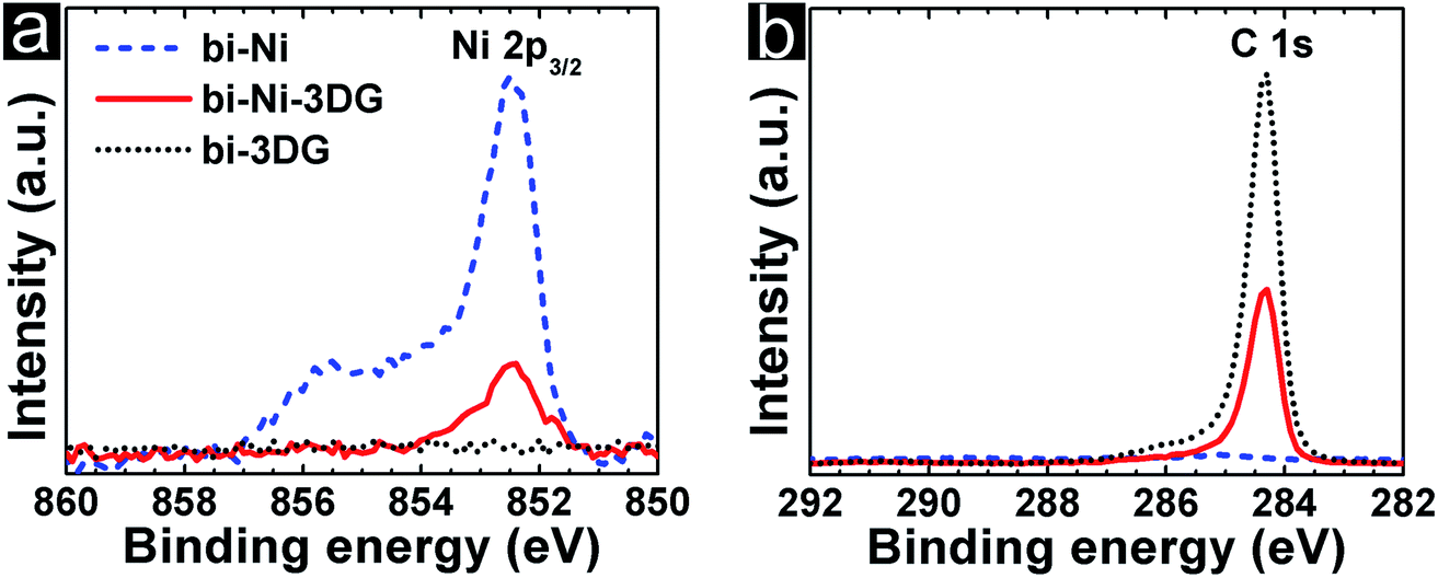 | ||
| Fig. 3 XPS spectra of the (a) Ni 2p peak and (b) C 1s peak of a bijel templated electroless Ni scaffold after thermal removal of PEGDA (blue curve), after CVD growth (red curve), and after etching Ni with FeCl3 (black curve). | ||
Deconvolution of the bi-3DG C 1s spectrum is performed to further analyze the chemical environment of carbon in the sample. Shirley background subtraction is performed and then the peak is fit with a Doniach–Sunjic (DS) line shape to model the C![[double bond, length as m-dash]](https://www.rsc.org/images/entities/char_e001.gif) C contribution68 (Fig. S2d and further discussion in ESI†). A Voigt line shape is used to model the C–O contribution at 286.1 eV which are attributed to the phenol groups.69 The complex plasmon spectra of graphitic materials results in satellites attributed to π–π* transitions,70,71 which are fitted here with a Gaussian line shape at 290.4 eV. The CC bonds account for 92% of the observed bonds in the deconvoluted C 1s peak for both the bi-Ni-3DG and bi-3DG samples (Fig. S2c and d, ESI†).
C contribution68 (Fig. S2d and further discussion in ESI†). A Voigt line shape is used to model the C–O contribution at 286.1 eV which are attributed to the phenol groups.69 The complex plasmon spectra of graphitic materials results in satellites attributed to π–π* transitions,70,71 which are fitted here with a Gaussian line shape at 290.4 eV. The CC bonds account for 92% of the observed bonds in the deconvoluted C 1s peak for both the bi-Ni-3DG and bi-3DG samples (Fig. S2c and d, ESI†).
Further analysis of the chemical environment of C bonds is performed using Raman spectroscopy. In order to get a representative view of samples, 30 different Raman spectra with 50 μm spacing are acquired on bi-Ni-3DG and bi-3DG samples (Fig. S3, ESI†). The average of this dataset is used to select a representative Raman spectra (Fig. 4a) for bi-Ni-3DG and bi-3DG. The two most intense features are observed at 1574 cm−1 ± 4 cm−1 and 2698 cm−1 ± 8 cm−1 for bi-Ni-3DG, with 1571 cm−1 ± 2 cm−1 and 2696 cm−1 ± 9 cm−1 observed for bi-3DG. These peaks are associated with the aromatic ring breathing mode and layer breathing mode and are referred to as the G band and 2D band, respectively. Interestingly, a peak associated with defects is not observed in the Raman spectra indicating weak disorder in the samples. The ratio of the intensity of the 2D and G bands (I2D/IG) is often used to estimate the number of graphene layers.72 The I2D/IG ratio decreases from 1.4 ± 1.2 for bi-Ni-3DG to 0.9 ± 0.6 for bi-3DG. This suggests that some graphene layers collapse onto each other after removal of the Ni scaffold support. While the average value of the I2D/IG ratio decreases after etching Ni there is still a 25% probability of observing ratios greater than 1 and the distribution is narrower indicating more uniformity across the sample.
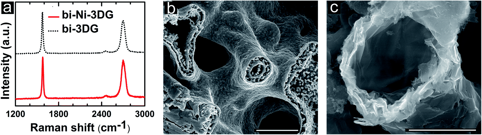 | ||
| Fig. 4 (a) Representative Raman spectra of graphene/Ni (red solid curve) and graphene (black dotted curve) bijel-templated architectures. (b) SEM cross sectional image of 3D Ni structure formed from a bijel template after pyrolysis of the Ni-coated PEGDA scaffold. The scale bar is 10 μm. (c) Cross-sectional SEM image of a pore within 3D graphene structure grown on Ni architecture. The scale bar is 4 μm. | ||
Characterization of graphene layer stacking
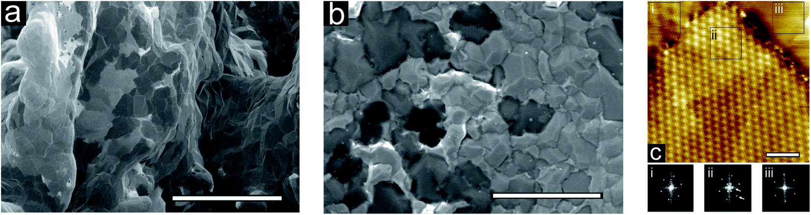
We further examine the full-width at half-maximum (FWHM) of I2D in the Raman spectra, which also provides information on the relative orientation of domains between layers.73 Layer stacking in multilayer graphene is typically AB (Bernal) but in some cases rotationally-faulted, i.e., turbostratic, stacking is also observed. Histograms for the measured I2D FWHM are shown in Fig. S3 of ESI.† While the average value of I2D FWHM observed before and after Ni etching is approximately the same, 55 cm−1, for bi-Ni-3DG and bi-3DG, the I2D FWHM distribution for bi-3DG (Fig. S3c, ESI†) shifts to a more clearly separated bimodal distribution with a large peak at 60 cm−1 and a secondary peak at 35 cm−1. The FWHM value at the secondary peak approaches that expected for single layer graphene (SLG) and indicates the presence of turbostratic graphene,67–69i.e., stacked graphene layers with relative misorientation with respect to Bernal stacking. Due to the decreased electronic coupling between layers, carrier mobility in turbostratic graphene can approach that of SLG.74,75 A FWHM of 60 cm−1 is associated with small misorientation angles of a few degrees. As the I2D FWHM reflects the misorientation between layers,72,74,75 it appears that there are primarily regions with small relative misorientation from Bernal stacked graphene and some regions with larger relative misorientation between layers after removal of the Ni scaffold. The higher spatial uniformity in the FWHM is also observed in the I2D/IG ratio of bi-3DG (Fig. S3c and d, ESI†) compared to bi-Ni-3DG (Fig. S3a and b, ESI†).In order to better understand this transition in Raman data that reflects layer stacking between bi-Ni-3DG and bi-3DG, the interior morphology of the structure is examined via SEM analysis of cleaved cross-sections. A cross section of a bi-Ni scaffold is shown in Fig. 4b. Multiple pore domains are observable, and in the center of the image, a circular pore is composed of two rings; each ring is comprised of a distinct, continuous Ni film approximately 300 nm thick, with dendritic features observed in between the rings. The second ring is attributed to the ultrasonication and low surface tension of the alcohol-based solution, which allows Ni ions to deposit into the PEGDA domains. After PEGDA is pyrolyzed, this deposited Ni segregates to form a second ring, as observed in Fig. 4b. The Ni scaffold is held at 800 °C for 30 minutes before CVD growth which is performed at 900 °C, so that the Ni scaffold further sinters into solid ligaments after CVD processing (shown in Fig. S5, ESI†). This mechanism is consistent with the 20% shrinkage of the structure observed in Fig. 1.
Each Ni surface in the porous channels of the 3D bi-Ni scaffold is a surface for CVD growth.76–78 The graphene layers form on all faces of the Ni surfaces, which then collapse onto one another upon removal of the Ni scaffold. This mechanism helps to explain why the I2D/IG ratios in the Raman spectra indicate an increase in the graphene layers from bi-Ni-3DG to bi-3DG. Fig. 4c shows a cross-sectional SEM image of bi-3DG with a pore in the center of the image where one may observe the graphene layer stacking with regions appearing extremely thin (transparent) to thick (opaque). While some wrinkles are observed in SEM images, the characteristic defect (D) band, typically found near 1350 cm−1 in Raman spectra, is not observed, indicating that there are few regions with sharp curvature.
In order to gain more insight into the graphene stacking in the 3D structures, we produce 2D graphene analogues (2DG) via EN deposition on modified SiO2 surfaces followed by CVD. This enables examination of the atomic structure of surfaces using scanning tunneling microscopy (STM). First, Raman measurements of the 2DG are acquired to compare the 2D analogues with bi-Ni-3DG samples. Both samples exhibit similar Raman spectra, indicating that 2DG (Fig. S4, ESI†) serves as a suitable analogue to gain insight on the atomic structure and morphology of the bi-Ni-3DG structures (Fig. S3a and b, ESI†).
Low-voltage SEM is used to compare the two samples; SEM images of bi-Ni-3DG and 2DG structures are shown in Fig. 5a and b, respectively. Regions of various contrasts are visible; the lighter contrast regions have previously been attributed to fewer graphene layers79,80 where the contrast variation has been related to the variation of work function with number of graphene layers.81 These micrographs provide further insight into the similarity of the graphene layer thicknesses and domain sizes between bi-Ni-3DG and 2DG.
 | ||
| Fig. 5 Low voltage SEM images acquired at 1 kV accelerating voltage of surfaces after CVD growth on (a) bijel-templated Ni architecture and (b) on a 2D substrate of Ni/SiO2/Si. The scale bar is 10 μm. (c) A 50 nm2 STM image shows various Moiré patterns on the 2D graphene film on Ni/SiO2/Si (empty states, I = 0.4 nA, Vgap = 400 mV). The scale bar is 10 nm. Fourier transforms are taken in the three regions highlighted in black boxes and labelled (i)–(iii), with their respective FFT shown below. | ||
We then characterize the 2DG sample with STM. A typical STM image is shown in Fig. 5c, where Moiré patterns are visible on the surface. Three regions with different Moiré patterns are highlighted in black boxes (labeled i, ii, and iii), and Fourier transforms of the measured atomic scale structure of the three regions are performed to elucidate the differences in periodicity. The Moiré pattern shown in Fig. 5c(i) depicts a graphene domain that is rotationally distinct from its neighbor, and a clear defect boundary demarks the transition from one domain into the other. The large domain in Fig. 5c(ii) clearly exhibits two different periodicities in its Fourier transform (indicated with white arrows), which suggest two rotationally offset graphene domains, both of which exist immediately below the uppermost surface layer. Fig. 5c(iii) exhibits yet another Moiré pattern, this time, a very high frequency one. The variety of Moiré patterns present on the surface suggests the dominant presence of randomly oriented graphene. Additional faint boundaries can be seen in the STM image, suggesting the presence of incommensurate sub-surface graphene layers. Although it is uncertain how deep these layers are, the fact that the visible Moiré patterns appear independent of these boundaries suggests that overall, the graphene layers are decoupled from each other and the Ni film, which is characteristic of turbostratic graphene that has been previously observed on polycrystalline Ni.82
It is interesting to pursue templates that promote the growth of turbostratic graphene with large domain sizes. Here, extended H2 annealing of the bi-Ni template is used to reduce the density of metal grain boundaries before CVD growth. It is known that large graphene domains can be produced by suppressing the number of graphene nucleation sites,83 such as metal grain boundaries,84 impurities,85 and defects,86 as well as CVD kinetics.85,87 After pyrolysis of PEGDA, a bi-Ni scaffold is annealed under low-pressure in forming gas for 30 min at 900 °C and cooled to room temperature. Afterwards, this annealed sample, referred to as bi-Ni-2, undergoes the same CVD growth steps as described earlier. Fig. 6a depicts representative Raman spectra of bi-Ni-2-3DG and bi-2-3DG; the average I2D/IG ratio is 1.3 ± 1.1 and 1.0 ± 0.5 and they have an average I2D FWHM of 61 cm−1 ± 16 cm−1 and 52 cm−1 ± 13 cm−1, respectively. The I2D FWHM has the highest probability density near 40 cm−1, a signature that a larger portion of the sample is composed of turbostratic stacking. Again, it is notable that there is no discernable defect peak. Compared with the bi-3DG sample (Fig. 4a), the average I2D/IG ratio for bi-2-3DG (Fig. 6a) increases and the standard deviation decreases. This trend is corroborated in histogram profiles of Raman spectroscopy data (Fig. S3e and f, ESI†). Overall, the histogram data corresponds to fewer layers of graphene in bi-2-3DG, more turbostratic regions, and a more uniform sample overall due to the larger Ni grains resulting from extended H2 anneal when compared to bi-3DG. Thus the ability of the bi-Ni scaffolds to withstand high thermal processing temperatures as presented here allows for tuning the microstructure on the metal scaffold in addition to CVD growth parameters to tune morphology of graphene architectures.
 | ||
| Fig. 6 (a) Representative Raman spectrum graphene/Ni (red solid curve) and graphene (black dotted curve) bijel-templated architectures where the nickel was annealed at 900 °C in forming gas before CVD growth. (b–d) SEM images of graphene bijel-templated architectures with scale bars of (b) 100 μm and (c and d) 10 μm. | ||
SEM images of bi-Ni-2-3DG are shown in Fig. 6b–d. Fig. 6b shows the preserved porous morphology in the sample. Here, the pore sizes observed are approximately 10–15 μm and smaller than those observed in bi-3DG (shown in Fig. 2c). The pore size reduction is attributed to additional sintering caused by pre-annealing of the bi-Ni-2 scaffold before CVD. Fig. 6c highlights a continuous wall in the bi-2-3DG sample where domains marked by faint contrast are visible and an average domain size of 3 μm is observed. Fig. 6d shows a cross-sectional view of the graphene material in a pore structure. The interconnectivity of the material in Fig. 6c and d appears to increase when compared to the distinct stacked flake morphology of Fig. 4c, which is no longer visible in the bi-2-3DG sample. Fig. 7 shows transmission electron microscopy (TEM) images of (a) bi-3DG and (b) bi-2-3DG. The thickness of the bi-3DG cross-section in Fig. 7a is approximately 44 nm whereas that of bi-2-3DG in Fig. 7c is approximately 22 nm, corresponding to 131 and 65 layers, respectively. A selected area electron diffraction indicates a periodicity of 0.333 nm, close to the expected periodicity of 0.335 for graphene. The insets are high-angle annular dark-field scanning transmission electron microscopy (HAADF-STEM) images included to more clearly view the contrast of the layers. The TEM, SEM and Raman data demonstrate that extended H2 anneal of the Ni scaffold improves the crystallinity and stacking of the 3D graphene architecture; larger domains are observed and fewer layers are evident by transparency in SEM images and increased I2D/IG ratios in the histogram profile (Fig. S3f†).
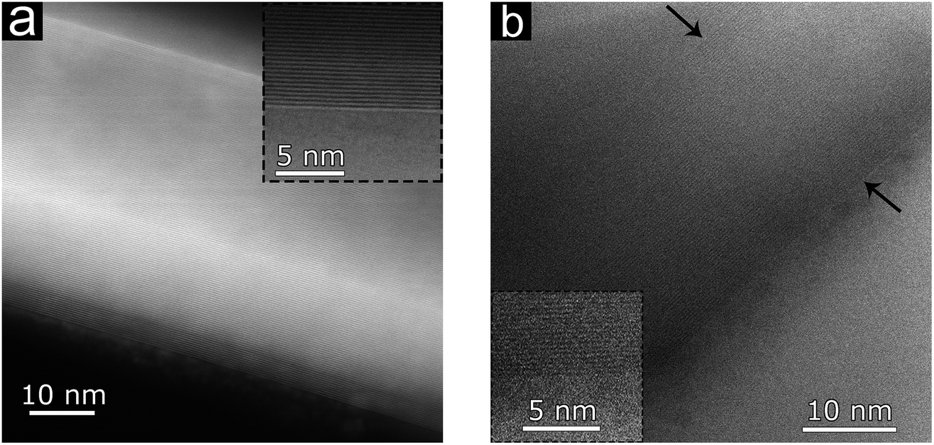 | ||
| Fig. 7 (a) Bright field TEM image of bi-3DG and (b) HAADF-STEM image of bi-2-3DG in cross section where the arrows highlight the edges of the cross-section in (b). The insets in (a) and (b) show a high-resolution view of layer stacking. | ||
Mechanical testing
The mechanical properties of a cellular material are governed by the topology of the architecture (i.e., the geometric distribution of matter within the volume of the porous material) and the mechanical properties of the base material. Gyroidal topologies are particularly robust, as their uniform negative Gaussian curvature throughout the channels yields highly uniform local stress distribution upon macroscopic deformation, resulting in exceptionally high stiffness and strength.88–91 Cellular materials based on spinodal shell architectures (nominally identical to those explored in this work) have been recently characterized numerically and experimentally, and shown to possess mechanical properties nearly identical to those of regular gyroid-inspired materials, in addition to displaying remarkable defect insensitivity (stemming from the stochastic nature of spinodal topologies).45 Most importantly, spinodal shell-based cellular materials can be fabricated in a uniquely scalable manner, as shown in previous work32,41,56 and this work. The combination of a spinodal shell-based architecture and a base material with superior in-plane intrinsic strength (such as graphene) could potentially result in a cellular material with exceptional mechanical properties.With this goal in mind, the mechanical properties of bi-3DG samples were evaluated via uniaxial compression with an Alemnis nanoindenter operated in displacement-control mode. A stress–strain curve obtained from a bi-3DG cylindrical sample with a diameter of 0.87 mm, a height of 1.24 mm, and a bulk density of 42 mg cm−3 is shown in Fig. 8a. A yield strength of approximately 130 kPa was measured, after which the sample displays a remarkably ductile and irreversible response upon compression. Notice that the response of bi-3DG pillars is significantly different from the classic compressive response of ceramic foams, which fail by progressive cracking of the base material, with visible stress drops,92 and much more similar to that of metallic systems. Intriguingly, the irreversible deformation beyond the linear elastic region is not characterized by a flat stress plateau, as commonly observed in elastic and plastic foams, but a region of continuous stress increase (akin to hardening in solid metals), accompanied by stiffening (see below). While this behavior has been observed multiple times in ultralight architected materials that deform reversibly by local buckling and/or localized fracture of the shell walls followed by extensive local rotations of ultra-thin ligaments with minimal local strains,93–96 it is not typically observed in architected materials that undergo irreversible deformations. While a full understanding of the internal deformation mechanisms that lead to this macroscopic behavior would require in situ characterization upon loading that are beyond the scope of this work, we interpret that the irreversible hardening/stiffening response of the bi-3DG material is due to sequential cracking/sliding of the graphene layers at a scale of the order of the characteristic length of the spinodal microstructure, followed by local densification.
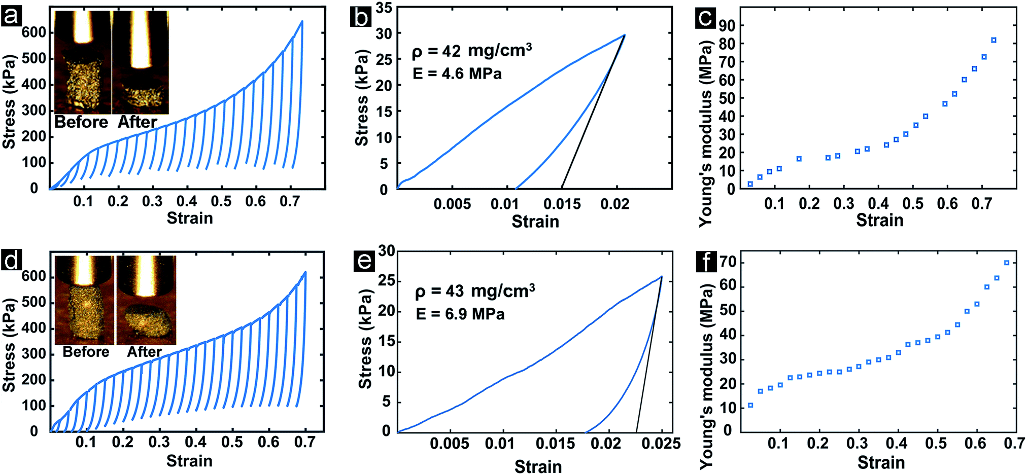 | ||
| Fig. 8 Nanoindentation measurements of a (a–c) graphene bijel-templated pillar with diameter 0.87 mm and height of 1.24 mm and of a (d–f) similar pillar, pre-annealed, with diameter 0.71 mm and height of 1.4 mm. (a and d) Stress–strain tests are performed on the same pillar with a strain rate of 1.2 μm s−1. Insets are before and after optical images of the graphene bijel-templated pillars. (b and e) Stress–strain curve acquired with a strain rate of 0.25 μm s−1. (c and f) Young's modulus vs. strain from the tests. | ||
Multiple loading–unloading curves were extracted and plotted in Fig. 8a to enable calculation of the Young's modulus (measured upon unloading, as illustrated in Fig. 8b) as a function of the macroscopically applied strain. The modulus versus strain evolution is depicted in Fig. 8c. Notice that the modulus is initially very low, 4 ± 1.3 MPa, as averaged over three nominally identical samples; this is attributed to the well-documented challenge in collecting modulus data at very low applied strain in ultra-light architected materials.45 At a strain of approximately 20%, the modulus stabilizes to a plateau value of 20 MPa. This value is taken as a reasonable estimate for the modulus of bi-3DG materials. At a strain of approximately 50%, the modulus starts increasing again with applied strain. This rise should not be attributed to densification, for two reasons: (i) densification in cellular materials occurs at compressive strains of the order of 1 − ε, with the relative density of the materials and ε = 1.5.97 While the relative density of these samples is not easy to measure, a rough estimate of 0.02 can be estimated by dividing the bulk density of the sample (42 mg cm−3) by the mass density of graphite (2260 mg cm−3). This value yields a calculated densification strain of approximately 97%, which is far higher than the approximately 50% strain at which the modulus starts increasing. (ii) The modulus at 70% strain is still orders of magnitude lower than that of solid graphene, or even graphite. As mentioned above, we tentatively attribute the rise in modulus with strain to localized fracture of the graphene layers and local rearrangement of the porous microstructure upon loading.
Mechanical tests are repeated on a bi-2-3DG pillar, and are shown in Fig. 8d–f. A plateau modulus of 30 MPa is extracted for this sample from Fig. 8f. This represents a 50% increase when compared to the bi-3DG sample, demonstrating the improvement in physical properties that occurs by increasing the grain size of the Ni scaffold. The increase in Young's modulus of bi-2-3DG over bi-3DG is tentatively attributed to increased interconnectivity of the graphene layers, as observed in the SEM image of Fig. 6c.
Table 1 displays these results in the context of other graphene-based foams previously reported in the literature, with recent work on similar architectures demonstrating CVD-derived graphene51 exhibits better mechanical properties than graphene architectures derived via other methods.52–55 Both the 3D bijel-template architectures are between 20 and 4000 times stiffer than previously reported graphene-based materials.52–55
Conclusions
A scalable method towards fabrication of free-standing gyroid-inspired turbostratic graphene architectures is demonstrated. The robust bijel templates allow the resultant graphene structures to retain minimal surface morphology with co-continuous pores, in agreement with theoretical results,98 despite the CVD processing temperatures necessary to produce high-quality graphene. Nanoindentation tests of mm-sized structures revealed one of the highest Young's moduli recorded for a free standing macroscopic porous monolith made of sp2 carbon, which is attributed to the minimal surface morphology. The suite of materials characterization techniques used, demonstrates the influence of the template on layer stacking in graphene films; statistical analysis of Raman data demonstrated an average I2D/IG of 1.0 achieved despite the multilayer structure of the graphene. The ability to fabricate monoliths composed of turbostratic graphene has interesting implications for electronic properties.99 Thus, the presented gyroid-inspired turbostratic graphene architectures are useful for applications where the electrical properties approaching SLG are desired in 3D devices, from the exploration of 3D spintronics,74 sensing applications,100 to energy systems.Experimental methods
Synthesis of bicontinuous interfacially jammed emulsion gel (bijel)
Poly(ethylene glycol) diacrylate bijel-based scaffolds (bi-PEGDA) are synthesized as described in a previous report32 and the process is briefly described here. Stöber process silica with controlled surface chemistry were dispersed via ultrasonic horn in deionized water (Millipore) and mixed with 2,6-lutidine (Sigma-Aldrich, St. Louis, MO, CAS #108-48-5), such that the respective volume fractions were 3.02%, 66.9%, and 30.1%. 205 ml samples were heated in a microwave for 30 s at a power of 160 W to induce spinodal decomposition of the water and oil, and then transferred to a 70 °C oven to maintain sample temperature above the critical point of 33.9 °C.101 35 μl of polyethylene glycol diacrylate 250 (PEGDA, Sigma Aldrich, St. Louis, MO, CAS #26570-48-9) is added to the top of each sample with 1 vol% Darocur 1173 (Ciba Specialty Chemicals, Basel, Switzerland) as a photoinitiator. The monomer diffused through the organic phase of the bijel for 4 hours before UV polymerization (Omnicure Series 1000, 100 W power). After curing, the templates were rinsed with DI water to remove unreacted monomer. Silica particles were etched from internal surfaces via 5 hour treatment with 6 M hydrofluoric acid (Fisher Scientific, Hampton, NH, CAS #7732-18-5). Excess acid is rinsed from the polymer template with DI water and the scaffold left to dry at 70 °C.Synthesis of bi-Ni
The bi-Ni scaffold is formed by electroless Ni (EN) deposition on bi-PEGDA followed by sintering under ambient conditions and then reducing in a vacuum environment to leave a freestanding bi-Ni scaffold as described in previous work.49 Briefly, bi-PEGDA templates are soaked in a supersaturated solution of palladium chloride (Sigma Aldrich, St. Louis, MO, CAS #7647-10-1) in alcohol overnight. The EN plating solution is 0.02 M nickel chloride hexahydrate (Fisher Scientific, Hampton, NH, CAS #7791-20-0), 0.02 M sodium tartrate dihydrate (Aldrich Chemical Company, Milwaukee, WI, CAS #6106-24-7), 1 M hydrazine (Sigma-Aldrich, St. Louis, MO, CAS #10217-52-4), and 1 vol% 1-propanol (Fisher Chemical, Waltham, MA, CAS #71-23-8). The pH of the EN solution is adjusted to an approximate value of 10 by addition of NaOH and maintained throughout the duration of the plating process with additional NaOH as necessary. The activated bi-PEGDA is cleaned in isopropanol (IPA). The temperature of the EN solution is controlled at 95 °C via immersion in a hot water bath. The EN solution is drained after 330 min and the scaffolds rinsed in IPA to remove unreacted salts. The scaffolds are heat-treated for 1 h at 300 °C and 1 h at 500 °C in air to remove the polymer template. The furnace is then purged with Ar and filled with forming gas (5% H2, 95% Ar) and the sample is heated at 450 °C for 8 h to reduce the oxidized Ni to its metallic state and sintered to impart structural integrity to the scaffold.Synthesis of 2-dimensional Ni thin films
Si wafers with a 300 nm SiO2 layer on the surface are treated with 5:1:1 DI:NH4OH:H2O2 at 70 °C (RCA-1) for 15 min, immersed in 3 separate DI baths, rinsed in flowing DI, and dried with N2 gas (Airgas). The wafers were immediately transferred into a 0.5 mmol (3-aminopropyl) triethoxysilane (APTES) (Sigma-Aldrich, St. Louis, MO, CAS #919-30-2) in DI water and left for 12–16 h. Afterwards, Si wafers are removed from the APTES solution, rinsed in a methanol stream and sonicated in methanol for 2 min. Si wafers are ethanol rinsed and activated in a solution of supersaturated palladium chloride in ethanol for at least 1 hour. Subsequently, EN deposition is performed as described in the above section with the addition of Tween 20 surfactant (Sigma-Aldrich, St. Louis, MO, CAS #9005-64-5) to reduce bubble-induced delamination on the EN surface. The resultant EN coated Si wafers were rinsed with ethanol and dried on a hot plate at 105 °C for 5 min.
Chemical vapor deposition of graphene
All samples were loaded into a 1′′ quartz tube and evacuated to a pressure of approximately 10−2 Torr while flowing forming gas (5% H2 in Ar) at 100 SCCM into the system. The furnace is purged under vacuum/forming gas for 1 h at ambient temperature, followed by a ramp to 800 °C at a rate of 10 °C min−1. The samples are held at 800 °C for 30 min. The furnace temperature is then increased to 900 °C at 10 °C min−1. At this point, 5 SCCM CH4 in 100 SCCM forming gas is introduced into the system for 30 min. Subsequently, CH4 is turned off and the furnace set to cool to room temperature at 10 °C min−1 under forming gas with no active cooling.Extended anneal of bi-Ni
For creating bi-Ni-2-3DG samples, bi-Ni samples were loaded into a 1′′ quartz tube and evacuated to a pressure of approximately 10−2 Torr while flowing forming gas at 100 SCCM into the system. The furnace is purged under vacuum/forming gas for 1 h at ambient temperature, followed by a ramp to 800 °C at a rate of 10 °C min−1. The samples are held at 800 °C for 30 min. The furnace temperature is then increased to 900 °C at 10 °C min−1 and held at 900 °C for 30 min followed by cooling (10 °C min−1) to room temperature, creating bi-Ni-2 CVD is then performed as described in “Chemical vapor deposition of graphene” to create bi-Ni-2-3DG.Freestanding bi-3DG
After CVD growth, bi-Ni-3DG are etched in 1 M FeCl3 aqueous solution at ambient temperature for 12 h. The resulting bi-3DG is then soaked in 3 separate dishes of DI for 5 min each followed by IPA for 5 min. Bi-3DG is then placed into a glass vial and dried on a hot plate at 130 °C for 30 min.Chemical and morphological characterization
Raman measurements were obtained on a Renishaw InVia Raman microscope with 532 nm incident laser. XPS measurements were performed with an AXIS Supra XPS by Kratos Analytical using a monochromated Al Kα radiation. Scanning electron microscopy images were acquired in a FEI/Philips XL30 FESEM at 10 kV and an FEI Quanta 3D FEG at 10 kV (Fig. 6b–d) and 30 kV (Fig. 4c). Low accelerating voltage images were taken in a FEI Magellan 400 XHR SEM at 1 kV with 3.0 m spot size, and 10 mm working distance. STM measurements were taken with an Omicron VT-SPM at room temperature and pressure of approximately 10−11 Torr. Samples were degassed for 24 h at 600 °C to remove surface adsorbates prior to scanning. Etched tungsten tips were used at a scanning voltage of 400 mV and tip-sample bias. Images were analyzed using Image Metrology's SPIP and Wolfram Mathematica. Nitrogen adsorption isotherms were performed by Micromeritics using a Micromeritics Tristar II Plus for specific surface area measurements. Transmission electron microscopy (TEM) was performed using a JEOL JEM-ARM300F Grand Arm TEM/STEM with 300 kV accelerating voltage to acquire both high-angle annular dark field-scanning TEM (HAADF-STEM) and bright field images.Density measurements
The height and diameter of bi-3DG and bi-2-3DG pillars were measured with SEM. A Sartorius ultra-microbalance (readability of up to 0.1 μg) was used to weigh the bi-3DG and bi-2-3DG. The density was calculated by dividing the mass by the bulk volume of the pillar.Mechanical characterization
Pillars of bi-3DG and bi-2-3DG with approximately 900 μm diameters were formed using 1 mm biopsy punch-outs to define a bi-PEGDA template with height of approximately 1.25 mm. After processing into bi-3DG or bi-2-3DG, the samples were mounted onto an Al SEM stub with double sided Cu tape. Compression tests were conducted using a commercial nanoindentor (Alemnis, Switzerland) with displacement-control function with a 1.4 mm stainless steel flat punch tip. In order to measure the Young's modulus, a constant strain rate of 0.25 μm s−1 is performed on 3 samples which were strained to approximately 3%. In addition, 26 cycles of loading and unloading were performed on a single sample which is compressed to 70% strain at a constant strain rate of 1.2 μm s−1. 0.2% offset yield strength is measured and Young's modulus at different strain was extracted from unloading curves. The experiments were performed under an optical microscope to record and observe the deformation of the structure during the tests.Conflicts of interest
There are no conflicts of interest to declare.Acknowledgements
This work was supported by the National Science Foundation under EECS-1449397 and CMMI-1301489. AEG thanks the U.S. Department of Education Graduate Assistance in Areas of National Need (GAANN) Fellowship and NSF for a Graduate Research Fellowship. CSW acknowledges funding from a NSF Graduate Research Fellowship. The authors acknowledge the technical support of Dr Mingjie Xu for acquisition of TEM images and Dr Li Xing for TEM sample preparation at the Irvine Materials Research Institute at UC Irvine. The authors also acknowledge the use of the facilities within the Laser Spectroscopy Facility for Raman spectroscopy and the Laboratory for Electron and X-ray Instrumentation (LEXI) center for X-ray photoelectron spectroscopy at UC Irvine.Notes and references
- T. Lin, I.-W. Chen, F. Liu, C. Yang, H. Bi, F. Xu and F. Huang, Nitrogen-doped mesoporous carbon of extraordinary capacitance for electrochemical energy storage, Science, 2015, 350, 1508–1513 CrossRef CAS PubMed.
- R. Kumar, J.-H. Oh, H.-J. Kim, J.-H. Jung, C.-H. Jung, W. G. Hong, H.-J. Kim, J.-Y. Park and I.-K. Oh, Nanohole-structured and palladium-embedded 3D porous graphene for ultrahigh hydrogen storage and CO oxidation multifunctionalities, ACS Nano, 2015, 9, 7343–7351 CrossRef CAS PubMed.
- Y. Yang, P. Li, S. Wu, X. Li, E. Shi, Q. Shen, D. Wu, W. Xu, A. Cao and Q. Yuan, Hierarchically Designed Three-Dimensional Macro/Mesoporous Carbon Frameworks for Advanced Electrochemical Capacitance Storage, Chem.–Eur. J., 2015, 21, 6157–6164 CrossRef CAS PubMed.
- Y. Yang, X. Yang, S. Chen, M. Zou, Z. Li, A. Cao and Q. Yuan, Rational design of hierarchical carbon/mesoporous silicon composite sponges as high-performance flexible energy storage electrodes, ACS Appl. Mater. Interfaces, 2017, 9, 22819–22825 CrossRef CAS PubMed.
- Y. Xue, D. Yu, L. Dai, R. Wang, D. Li, A. Roy, F. Lu, H. Chen, Y. Liu and J. Qu, Three-dimensional B, N-doped graphene foam as a metal-free catalyst for oxygen reduction reaction, Phys. Chem. Chem. Phys., 2013, 15, 12220–12226 RSC.
- X. Dong, Y. Cao, J. Wang, M. B. Chan-Park, L. Wang, W. Huang and P. Chen, Hybrid structure of zinc oxide nanorods and three dimensional graphene foam for supercapacitor and electrochemical sensor applications, RSC Adv., 2012, 2, 4364–4369 RSC.
- N. Li, Q. Zhang, S. Gao, Q. Song, R. Huang, L. Wang, L. Liu, J. Dai, M. Tang and G. Cheng, Three-dimensional graphene foam as a biocompatible and conductive scaffold for neural stem cells, Sci. Rep., 2013, 3, 1604 CrossRef PubMed.
- H. Amani, E. Mostafavi, H. Arzaghi, S. Davaran, A. Akbarzadeh, O. Akhavan, H. Pazoki-Toroudi and T. J. Webster, Three-dimensional graphene foams: synthesis, properties, biocompatibility, biodegradability, and applications in tissue engineering, ACS Biomater. Sci. Eng., 2018, 5, 193–214 CrossRef.
- X. Du, I. Skachko, A. Barker and E. Y. Andrei, Approaching ballistic transport in suspended graphene, Nat. Nanotechnol., 2008, 3, 491–495 CrossRef CAS PubMed.
- A. A. Balandin, S. Ghosh, W. Bao, I. Calizo, D. Teweldebrhan, F. Miao and C. N. Lau, Superior thermal conductivity of single-layer graphene, Nano Lett., 2008, 8, 902–907 CrossRef CAS PubMed.
- C. Lee, X. Wei, J. W. Kysar and J. Hone, Measurement of the elastic properties and intrinsic strength of monolayer graphene, Science, 2008, 321, 385–388 CrossRef CAS PubMed.
- G.-H. Lee, R. C. Cooper, S. J. An, S. Lee, A. Van Der Zande, N. Petrone, A. G. Hammerberg, C. Lee, B. Crawford and W. Oliver, High-strength chemical-vapor-deposited graphene and grain boundaries, Science, 2013, 340, 1073–1076 CrossRef CAS PubMed.
- D. Cohen-Tanugi and J. C. Grossman, Mechanical strength of nanoporous graphene as a desalination membrane, Nano Lett., 2014, 14, 6171–6178 CrossRef CAS PubMed.
- M. D. Stoller, S. Park, Y. Zhu, J. An and R. S. Ruoff, Graphene-based ultracapacitors, Nano Lett., 2008, 8, 3498–3502 CrossRef CAS PubMed.
- H. Wang, Y. Yang, Y. Liang, J. T. Robinson, Y. Li, A. Jackson, Y. Cui and H. Dai, Graphene-wrapped sulfur particles as a rechargeable lithium–sulfur battery cathode material with high capacity and cycling stability, Nano Lett., 2011, 11, 2644–2647 CrossRef CAS PubMed.
- Z. Chen, C. Xu, C. Ma, W. Ren and H.-M. Cheng, Lightweight and flexible graphene foam composites for high-performance electromagnetic interference shielding, Adv. Mater., 2013, 25, 1296–1300 CrossRef CAS PubMed.
- H. Hu, Z. Zhao, W. Wan, Y. Gogotsi and J. Qiu, Ultralight and highly compressible graphene aerogels, Adv. Mater., 2013, 25, 2219–2223 CrossRef CAS PubMed.
- G. K. Dimitrakakis, E. Tylianakis and G. E. Froudakis, Pillared Graphene: A New 3-D Network Nanostructure for Enhanced Hydrogen Storage, Nano Lett., 2008, 8, 3166–3170 CrossRef CAS PubMed.
- Y. Yang, W. Yin, S. Wu, X. Yang, W. Xia, Y. Shen, Y. Huang, A. Cao and Q. Yuan, Perovskite-Type LaSrMnO Electrocatalyst with Uniform Porous Structure for an Efficient Li–O2 Battery Cathode, ACS Nano, 2015, 10, 1240–1248 CrossRef PubMed.
- W. Jiang, H. Xin and W. Li, Microcellular 3D graphene foam via chemical vapor deposition of electroless plated nickel foam templates, Mater. Lett., 2016, 162, 105–109 CrossRef CAS.
- X. Cao, Y. Shi, W. Shi, G. Lu, X. Huang, Q. Yan, Q. Zhang and H. Zhang, Preparation of Novel 3D Graphene Networks for Supercapacitor Applications, Small, 2011, 7, 3163–3168 CrossRef CAS PubMed.
- G. Hu, C. Xu, Z. Sun, S. Wang, H.-M. Cheng, F. Li and W. Ren, 3D Graphene-Foam-Reduced-Graphene-Oxide Hybrid Nested Hierarchical Networks for High-Performance Li–S Batteries, Adv. Mater., 2016, 28, 1603–1609 CrossRef CAS PubMed.
- Z. Chen, W. Ren, L. Gao, B. Liu, S. Pei and H.-M. Cheng, Three-dimensional flexible and conductive interconnected graphene networks grown by chemical vapour deposition, Nat. Mater., 2011, 10, 424 CrossRef CAS PubMed.
- X. Dong, Y. Ma, G. Zhu, Y. Huang, J. Wang, M. B. Chan-Park, L. Wang, W. Huang and P. Chen, Synthesis of graphene–carbon nanotube hybrid foam and its use as a novel three-dimensional electrode for electrochemical sensing, J. Mater. Chem., 2012, 22, 17044 RSC.
- J. Ning, X. Xu, C. Liu and D. L. Fan, Three-dimensional multilevel porous thin graphite nanosuperstructures for Ni(OH)2 -based energy storage devices, J. Mater. Chem. A, 2014, 2, 15768–15773 RSC.
- E. Singh, Z. Chen, F. Houshmand, W. Ren, Y. Peles, H.-M. Cheng and N. Koratkar, Superhydrophobic Graphene Foams, Small, 2013, 9, 75–80 CrossRef CAS PubMed.
- H. Hui, R. Xia, J. Li, Q. Mei, Y. Ma, F. Chen and Y. Lei, Effects of Cold Rolling and Annealing Prior to Dealloying on the Microstructure of Nanoporous Gold, Nanomaterials, 2018, 8, 540 CrossRef PubMed.
- Y. Ito, Y. Tanabe, H.-J. Qiu, K. Sugawara, S. Heguri, N. H. Tu, K. K. Huynh, T. Fujita, T. Takahashi, K. Tanigaki and M. Chen, High-Quality Three-Dimensional Nanoporous Graphene, Angew. Chem., 2014, 126, 4922–4926 CrossRef.
- H.-J. Qiu, J. Q. Wang, P. Liu, Y. Wang and M. W. Chen, Hierarchical nanoporous metal/metal-oxide composite by dealloying metallic glass for high-performance energy storage, Corros. Sci., 2015, 96, 196–202 CrossRef CAS.
- M. Mokhtari, C. Le Bourlot, J. Adrien, S. Dancette, T. Wada, J. Duchet-Rumeau, H. Kato and E. Maire, Cold-rolling influence on microstructure and mechanical properties of NiCr–Ag composites and porous NiCr obtained by liquid metal dealloying, J. Alloys Compd., 2017, 707, 251–256 CrossRef CAS.
- F. Liu, C. Wang and Q. Tang, Conductivity Maximum in 3D Graphene Foams, Small, 2018, 14, 1801458 CrossRef PubMed.
- M. N. Lee and A. Mohraz, Bicontinuous macroporous materials from bijel templates, Adv. Mater., 2010, 22, 4836–4841 CrossRef CAS PubMed.
- K. Stratford, R. Adhikari, I. Pagonabarraga, J.-C. Desplat and M. E. Cates, Colloidal Jamming at Interfaces: A Route to Fluid-Bicontinuous Gels, Science, 2005, 309, 2198–2201 CrossRef CAS PubMed.
- M. Reeves, K. Stratford and J. H. Thijssen, Quantitative morphological characterization of bicontinuous Pickering emulsions via interfacial curvatures, Soft Matter, 2016, 12, 4082–4092 RSC.
- J. M. Carmack and P. C. Millett, Tuning thin-film bijels with applied external electric fields, Soft Matter, 2018, 14, 4344–4354 RSC.
- A. H. Schoen, Infinite periodic minimal surfaces without intersections, NASA Technical Note TD-5541, 1970 Search PubMed.
- E. M. Herzig, K. A. White, A. B. Schofield, W. C. K. Poon and P. S. Clegg, Bicontinuous emulsions stabilized solely by colloidal particles, Nat. Mater., 2007, 6, 966 CrossRef CAS PubMed.
- J. A. Witt, D. R. Mumm and A. Mohraz, Bijel reinforcement by droplet bridging: a route to bicontinuous materials with large domains, Soft Matter, 2013, 9, 6773–6780 RSC.
- Y. Nishikawa, H. Jinnai, T. Koga, T. Hashimoto and S. T. Hyde, Measurements of Interfacial Curvatures of Bicontinuous Structure from Three-Dimensional Digital Images. 1. A Parallel Surface Method, Langmuir, 1998, 14, 1242–1249 CrossRef CAS.
- M. E. Cates and P. S. Clegg, Bijels: a new class of soft materials, Soft Matter, 2008, 4, 2132–2138 RSC.
- M. N. Lee, J. H. J. Thijssen, J. A. Witt, P. S. Clegg and A. Mohraz, Making a Robust Interfacial Scaffold: Bijel Rheology and its Link to Processability, Adv. Funct. Mater., 2013, 23, 417–423 CrossRef CAS.
- A. Koponen, M. Kataja and J. v. Timonen, Tortuous flow in porous media, Phys. Rev. E: Stat. Phys., Plasmas, Fluids, Relat. Interdiscip. Top., 1996, 54, 406 CrossRef CAS.
- K. Jurewicz, C. Vix-Guterl, E. Frackowiak, S. Saadallah, M. Reda, J. Parmentier, J. Patarin and F. Béguin, Capacitance properties of ordered porous carbon materials prepared by a templating procedure, J. Phys. Chem. Solids, 2004, 65, 287–293 CrossRef CAS.
- K. Yuan, Y. Xu, J. Uihlein, G. Brunklaus, L. Shi, R. Heiderhoff, M. Que, M. Forster, T. Chassé, T. Pichler, T. Riedl, Y. Chen and U. Scherf, Straightforward Generation of Pillared, Microporous Graphene Frameworks for Use in Supercapacitors, Adv. Mater., 2015, 27, 6714–6721 CrossRef CAS PubMed.
- M.-T. Hsieh, B. Endo, Y. Zhang, J. Bauer and L. Valdevit, The mechanical response of cellular materials with spinodal topologies, J. Mech. Phys. Solids, 2019, 125, 401–419 CrossRef.
- H.-Y. Chen, Y. Kwon and K. Thornton, Multifunctionality of three-dimensional self-assembled composite structure, Scr. Mater., 2009, 61, 52–55 CrossRef CAS.
- T. Cebo, A. I. Aria, J. A. Dolan, R. S. Weatherup, K. Nakanishi, P. R. Kidambi, G. Divitini, C. Ducati, U. Steiner and S. Hofmann, Chemical vapour deposition of freestanding sub-60 nm graphene gyroids, Appl. Phys. Lett., 2017, 111, 253103 CrossRef.
- L. Imperiali, C. Clasen, J. Fransaer, C. W. Macosko and J. Vermant, A simple route towards graphene oxide frameworks, Mater. Horiz., 2014, 1, 139–145 RSC.
- S. Ye, J. Feng and P. Wu, Deposition of three-dimensional graphene aerogel on nickel foam as a binder-free supercapacitor electrode, ACS Appl. Mater. Interfaces, 2013, 5, 7122–7129 CrossRef CAS.
- R. M. Hensleigh, H. Cui, J. S. Oakdale, C. Y. Jianchao, P. G. Campbell, E. B. Duoss, C. M. Spadaccini, X. Zheng and M. A. Worsley, Additive manufacturing of complex micro-architected graphene aerogels, Mater. Horiz., 2018, 5, 1035–1041 RSC.
- H. Kashani, Y. Ito, J. Han, P. Liu and M. Chen, Extraordinary tensile strength and ductility of scalable nanoporous graphene, Sci. Adv., 2019, 5, eaat6951 CrossRef PubMed.
- A. Nieto, B. Boesl and A. Agarwal, Multi-scale intrinsic deformation mechanisms of 3D graphene foam, Carbon, 2015, 85, 299–308 CrossRef CAS.
- L. Lv, P. Zhang, H. Cheng, Y. Zhao, Z. Zhang, G. Shi and L. Qu, Solution-Processed Ultraelastic and Strong Air-Bubbled Graphene Foams, Small, 2016, 12, 3229–3234 CrossRef CAS PubMed.
- H. Sun, Z. Xu and C. Gao, Multifunctional, ultra-flyweight, synergistically assembled carbon aerogels, Adv. Mater., 2013, 25, 2554–2560 CrossRef CAS PubMed.
- Y. Li, J. Chen, L. Huang, C. Li, J.-D. Hong and G. Shi, Highly compressible macroporous graphene monoliths via an improved hydrothermal process, Adv. Mater., 2014, 26, 4789–4793 CrossRef CAS PubMed.
- J. A. Witt, D. R. Mumm and A. Mohraz, Microstructural tunability of co-continuous bijel-derived electrodes to provide high energy and power densities, J. Mater. Chem. A, 2016, 4, 1000–1007 RSC.
- H.-Y. Hsueh, Y.-C. Huang, R.-M. Ho, C.-H. Lai, T. Makida and H. Hasegawa, Nanoporous gyroid nickel from block copolymer templates via electroless plating, Adv. Mater., 2011, 23, 3041–3046 CrossRef CAS.
- S. S. Sundarram, W. Jiang and W. Li, Fabrication of small pore-size nickel foams using electroless plating of solid-state foamed immiscible polymer blends, J. Manuf. Sci. Eng., 2014, 136, 021002 CrossRef.
- S. Sotiropoulos, I. J. Brown, G. Akay and E. Lester, Nickel incorporation into a hollow fibre microporous polymer: a preparation route for novel high surface area nickel structures, Mater. Lett., 1998, 35, 383–391 CrossRef CAS.
- J. R. Rostrup-Nielsen, K. Pedersen and J. Sehested, High temperature methanation: Sintering and structure sensitivity, Appl. Catal., A, 2007, 330, 134–138 CrossRef CAS.
- X. He, H. Zhang, H. Zhang, X. Li, N. Xiao and J. Qiu, Direct synthesis of 3D hollow porous graphene balls from coal tar pitch for high performance supercapacitors, J. Mater. Chem. A, 2014, 2, 19633–19640 RSC.
- L. Wang, Z. Sofer, A. Ambrosi, P. Šimek and M. Pumera, 3D-graphene for electrocatalysis of oxygen reduction reaction: Increasing number of layers increases the catalytic effect, Electrochem. Commun., 2014, 46, 148–151 CrossRef CAS.
- M. A. Worsley, P. J. Pauzauskie, T. Y. Olson, J. Biener, J. H. Satcher Jr and T. F. Baumann, Synthesis of graphene aerogel with high electrical conductivity, J. Am. Chem. Soc., 2010, 132, 14067–14069 CrossRef CAS PubMed.
- X. Zhang, Z. Sui, B. Xu, S. Yue, Y. Luo, W. Zhan and B. Liu, Mechanically strong and highly conductive graphene aerogel and its use as electrodes for electrochemical power sources, J. Mater. Chem., 2011, 21, 6494–6497 RSC.
- W. Li, S. Gao, L. Wu, S. Qiu, Y. Guo, X. Geng, M. Chen, S. Liao, C. Zhu and Y. Gong, High-density three-dimension graphene macroscopic objects for high-capacity removal of heavy metal ions, Sci. Rep., 2013, 3, 2125 CrossRef.
- H. Wang, D. Zhang, T. Yan, X. Wen, J. Zhang, L. Shi and Q. Zhong, Three-dimensional macroporous graphene architectures as high performance electrodes for capacitive deionization, J. Mater. Chem. A, 2013, 1, 11778–11789 RSC.
- J. C. Lascovich, R. Giorgi and S. Scaglione, Evaluation of the sp2/sp3 ratio in amorphous carbon structure by XPS and XAES, Appl. Surf. Sci., 1991, 47, 17–21 CrossRef CAS.
- S. Doniach and M. Sunjic, Many-electron singularity in X-ray photoemission and X-ray line spectra from metals, J. Phys. C: Solid State Phys., 1970, 3, 285 CrossRef CAS.
- H. P. Boehm, Surface oxides on carbon and their analysis: a critical assessment, Carbon, 2002, 40, 145–149 CrossRef CAS.
- M. Guzzo, J. J. Kas, L. Sponza, C. Giorgetti, F. Sottile, D. Pierucci, M. G. Silly, F. Sirotti, J. J. Rehr and L. Reining, Multiple satellites in materials with complex plasmon spectra: From graphite to graphene, Phys. Rev. B: Condens. Matter Mater. Phys., 2014, 89, 085425 CrossRef.
- A. Kumar, A. A. Voevodin, D. Zemlyanov, D. N. Zakharov and T. S. Fisher, Rapid synthesis of few-layer graphene over Cu foil, Carbon, 2012, 50, 1546–1553 CrossRef CAS.
- A. C. Ferrari, J. C. Meyer, V. Scardaci, C. Casiraghi, M. Lazzeri, F. Mauri, S. Piscanec, D. Jiang, K. S. Novoselov, S. Roth and A. K. Geim, Raman Spectrum of Graphene and Graphene Layers, Phys. Rev. Lett., 2006, 97, 187401 CrossRef CAS PubMed.
- A. C. Ferrari, Raman spectroscopy of graphene and graphite: Disorder, electron–phonon coupling, doping and nonadiabatic effects, Solid State Commun., 2007, 143, 47–57 CrossRef CAS.
- N. Richter, Y. R. Hernandez, S. Schweitzer, J.-S. Kim, A. K. Patra, J. Englert, I. Lieberwirth, A. Liscio, V. Palermo and X. Feng, Robust two-dimensional electronic properties in three-dimensional microstructures of rotationally stacked turbostratic graphene, Phys. Rev. Appl., 2017, 7, 024022 CrossRef.
- J. A. Garlow, L. K. Barrett, L. Wu, K. Kisslinger, Y. Zhu and J. F. Pulecio, Large-area growth of turbostratic graphene on Ni (111) via physical vapor deposition, Sci. Rep., 2016, 6, 19804 CrossRef CAS PubMed.
- X. Li, W. Cai, L. Colombo and R. S. Ruoff, Evolution of graphene growth on Ni and Cu by carbon isotope labeling, Nano Lett., 2009, 9, 4268–4272 CrossRef CAS PubMed.
- S. J. Chae, F. Güneş, K. K. Kim, E. S. Kim, G. H. Han, S. M. Kim, H.-J. Shin, S.-M. Yoon, J.-Y. Choi and M. H. Park, Synthesis of large-area graphene layers on poly-nickel substrate by chemical vapor deposition: wrinkle formation, Adv. Mater., 2009, 21, 2328–2333 CrossRef CAS.
- L. Baraton, Z. B. He, C. S. Lee, C. S. Cojocaru, M. Châtelet, J.-L. Maurice, Y. H. Lee and D. Pribat, On the mechanisms of precipitation of graphene on nickel thin films, Europhys. Lett., 2011, 96, 46003 CrossRef.
- X. Li, W. Cai, J. An, S. Kim, J. Nah, D. Yang, R. Piner, A. Velamakanni, I. Jung and E. Tutuc, Large-area synthesis of high-quality and uniform graphene films on copper foils, Science, 2009, 324, 1312–1314 CrossRef CAS PubMed.
- K. Shihommatsu, J. Takahashi, Y. Momiuchi, Y. Hoshi, H. Kato and Y. Homma, Formation Mechanism of Secondary Electron Contrast of Graphene Layers on a Metal Substrate, ACS Omega, 2017, 2, 7831–7836 CrossRef CAS PubMed.
- M.-H. Park, T.-H. Kim and C.-W. Yang, Thickness contrast of few-layered graphene in SEM, Surf. Interface Anal., 2012, 44, 1538–1541 CrossRef CAS.
- Y. Zhang, T. Gao, S. Xie, B. Dai, L. Fu, Y. Gao, Y. Chen, M. Liu and Z. Liu, Different growth behaviors of ambient pressure chemical vapor deposition graphene on Ni (111) and Ni films: A scanning tunneling microscopy study, Nano Res., 2012, 5, 402–411 CrossRef CAS.
- G. H. Han, F. Gunes, J. J. Bae, E. S. Kim, S. J. Chae, H.-J. Shin, J.-Y. Choi, D. Pribat and Y. H. Lee, Influence of copper morphology in forming nucleation seeds for graphene growth, Nano Lett., 2011, 11, 4144–4148 CrossRef CAS PubMed.
- A. Reina, X. Jia, J. Ho, D. Nezich, H. Son, V. Bulovic, M. S. Dresselhaus and J. Kong, Large Area, Few-Layer Graphene Films on Arbitrary Substrates by Chemical Vapor Deposition, Nano Lett., 2009, 9, 30–35 CrossRef CAS.
- Y. Zhang, L. Gomez, F. N. Ishikawa, A. Madaria, K. Ryu, C. Wang, A. Badmaev and C. Zhou, Comparison of graphene growth on single-crystalline and polycrystalline Ni by chemical vapor deposition, J. Phys. Chem. Lett., 2010, 1, 3101–3107 CrossRef CAS.
- M. Losurdo, M. M. Giangregorio, P. Capezzuto and G. Bruno, Graphene CVD growth on copper and nickel: role of hydrogen in kinetics and structure, Phys. Chem. Chem. Phys., 2011, 13, 20836–20843 RSC.
- W. Liu, C.-H. Chung, C.-Q. Miao, Y.-J. Wang, B.-Y. Li, L.-Y. Ruan, K. Patel, Y.-J. Park, J. Woo and Y.-H. Xie, Chemical vapor deposition of large area few layer graphene on Si catalyzed with nickel films, Thin Solid Films, 2010, 518, S128–S132 CrossRef CAS.
- O. Al-Ketan, R. Rezgui, R. Rowshan, H. Du, N. X. Fang and R. K. Abu Al-Rub, Microarchitected Stretching-Dominated Mechanical Metamaterials with Minimal Surface Topologies, Adv. Eng. Mater., 2018, 1800029 CrossRef.
- I. Maskery, L. Sturm, A. O. Aremu, A. Panesar, C. B. Williams, C. J. Tuck, R. D. Wildman, I. A. Ashcroft and R. J. Hague, Insights into the mechanical properties of several triply periodic minimal surface lattice structures made by polymer additive manufacturing, Polymer, 2018, 152, 62–71 CrossRef CAS.
- D. W. Abueidda, M. Bakir, R. K. A. Al-Rub, J. S. Bergström, N. A. Sobh and I. Jasiuk, Mechanical properties of 3D printed polymeric cellular materials with triply periodic minimal surface architectures, Mater. Des., 2017, 122, 255–267 CrossRef CAS.
- Z. Qin, G. S. Jung, M. J. Kang and M. J. Buehler, The mechanics and design of a lightweight three-dimensional graphene assembly, Sci. Adv., 2017, 3, e1601536 CrossRef PubMed.
- L. J. Gibson and M. F. Ashby, Cellular solids: structure and properties, Cambridge University Press, 1999 Search PubMed.
- T. A. Schaedler, A. J. Jacobsen, A. Torrents, A. E. Sorensen, J. Lian, J. R. Greer, L. Valdevit and W. B. Carter, Ultralight metallic microlattices, Science, 2011, 334, 962–965 CrossRef CAS PubMed.
- A. Torrents, T. A. Schaedler, A. J. Jacobsen, W. B. Carter and L. Valdevit, Characterization of nickel-based microlattice materials with structural hierarchy from the nanometer to the millimeter scale, Acta Mater., 2012, 60, 3511–3523 CrossRef CAS.
- K. J. Maloney, C. S. Roper, A. J. Jacobsen, W. B. Carter, L. Valdevit and T. A. Schaedler, Microlattices as architected thin films: Analysis of mechanical properties and high strain elastic recovery, APL Mater., 2013, 1, 022106 CrossRef.
- L. R. Meza, S. Das and J. R. Greer, Strong, lightweight, and recoverable three-dimensional ceramic nanolattices, Science, 2014, 345, 1322–1326 CrossRef CAS PubMed.
- M. F. Ashby, T. Evans, N. A. Fleck, J. W. Hutchinson, H. N. G. Wadley and L. J. Gibson, Metal foams: a design guide, Elsevier, 2000 Search PubMed.
- G. S. Jung and M. J. Buehler, Multiscale Mechanics of Triply Periodic Minimal Surfaces of Three-Dimensional Graphene Foams, Nano Lett., 2018, 18, 4845–4853 CrossRef CAS PubMed.
- I. Di Bernardo, G. Avvisati, C. Mariani, N. Motta, C. Chen, J. Avila, M. C. Asensio, S. Lupi, Y. Ito and M. Chen, Two-dimensional hallmark of highly interconnected three-dimensional nanoporous graphene, ACS Omega, 2017, 2, 3691–3697 CrossRef CAS PubMed.
- X.-B. Hu, Y.-L. Liu, W.-J. Wang, H.-W. Zhang, Y. Qin, S. Guo, X.-W. Zhang, L. Fu and W.-H. Huang, Biomimetic Graphene-Based 3D Scaffold for Long-Term Cell Culture and Real-Time Electrochemical Monitoring, Anal. Chem., 2018, 90, 1136–1141 CrossRef CAS.
- A. Loven and O. Rice, Coexistence curve of the 2,6-lutidine + water system in the critical region, Trans. Faraday Soc., 1963, 59, 2723–2727 RSC.
Footnote |
| † Electronic supplementary information (ESI) available: Scanning electron microscopy images of sample cross sections, statistical analysis of Raman spectroscopy data, and X-ray photoelectron spectroscopy data after different sample processing steps. See DOI: 10.1039/c9na00358d |
| This journal is © The Royal Society of Chemistry 2019 |