
 Open Access Article
 This Open Access Article is licensed under a Creative Commons Attribution-Non Commercial 3.0 Unported Licence
Generation and enhancement of surface acoustic waves on a highly doped p-type GaAs substrate
Boqun
Dong
 * and
Mona E.
Zaghloul
* and
Mona E.
Zaghloul
Department of Electrical and Computer Engineering, The George Washington University, 800 22nd St NW, Washington, DC, USA. E-mail: dongbq@gwmail.gwu.edu
First published on 20th July 2019
Abstract
Surface acoustic waves (SAWs) have been widely studied due to their unique advantage to couple the mechanical, electrical, and optical characteristics of semiconductor materials and have successfully been used in many industrial applications. In this work, we report a design that uses piezoelectric material Zinc Oxide (ZnO) to enhance the generation and propagation of SAWs on the surface of a highly doped p-type Gallium Arsenide (GaAs) substrate, which is more extensively used in optoelectronic devices than intrinsic GaAs structures. To maximize the piezoelectricity and successfully generate SAWs, high quality c-axis orientation of the ZnO film is needed; thus we experiment and develop optimized recipes of a radio frequency (RF) magnetron sputtering system to deposit ZnO on the GaAs substrate. To further optimize the SAW performance, an intermediate Silicon Oxide (SiO2) layer is added between the ZnO film and GaAs substrate. Additionally, we test samples with varied thickness of ZnO films and dimensions of interdigital transducer (IDT) fingers to figure out their individual effect on SAW properties. The results and techniques demonstrated in this paper will provide guidance for further studies on enhancing SAWs propagating along many other doped semiconductor materials. This combination of acoustics and optoelectronics in doped semiconductors is a promising start to building enhanced and hybrid devices in various fields.
1 Introduction
Gallium Arsenide (GaAs) has been widely used in optoelectronic devices such as photodetectors, solar cells and photocathodes due to its outstanding photoelectric and photovoltaic properties.1–4 Recent research has shown that the optoelectronic performance of GaAs will be significantly improved by using surface acoustic waves (SAWs).5–7 A SAW is generated and propagated on the GaAs surface with the help of interdigital transducers (IDTs) and applied radio frequency AC voltage. This applied periodical potential will deform the crystal lattice of GaAs and bend the energy levels up and down, and therefore forcefully suppress the recombination probability of electrons and holes by spatially separating them. As a result, it helps improve the conversion efficiency of photon energy and the quantum efficiency (QE) in many GaAs applications.7–10 Previous work from Hernandez-Minguez and his colleagues suggested that applying SAWs can help realize the high-frequency (GHz) operation of carriers in nanowires of optoelectronic devices.11 Hermelin et al. demonstrated that with the help of SAWs the transportation of a single electron can be faster and more reliable between two distant quantum dots.12 Although researchers have successfully utilized SAWs in intrinsic GaAs devices to build hybrid structures, generating SAWs on doped GaAs has not been achieved so far.Doping of GaAs is commonly used in applications in the optoelectronic field and is an essential method for achieving better photoelectric performance. Therefore, improving the compatibility between doped GaAs and SAWs has been an important research topic in order to widely extend the application range of SAWs in optical and electronic devices. To achieve the generation and propagation of SAWs on the doped GaAs surface, two key factors need to be considered and resolved. First, the piezoelectric coupling coefficient of GaAs is much smaller than those of commonly used piezoelectric materials such as ZnO, LiNbO3 and AlN; thus only weak SAWs can be generated.13–15 Second, when a piezoelectric substrate, in this case, GaAs, has been doped, the concentration of free carriers increases, leading to an electrical screening of the radio frequency field applied on the IDTs, and results in a restraint of the generation of SAWs.7,16,17 To resolve this electrical screening issue, researchers such as J. Rudolph et al.16 and A. Violante et al.7 both came up with a similar method to place the doped layer away from the surface layers where SAWs were generated and propagated. A recent solution from Yuan and his colleagues is to add a metal layer on top of undoped GaAs/AlGaAs heterostructures on an n-type doped GaAs substrate (note that the undoped GaAs/AlGaAs layers covered the whole n-doped GaAs, but the metal layer did not). They used this metal layer to electrically screen the piezoelectric field of SAWs so that the SAWs can travel and reach the GaAs in a mechanical way.17
In this present work, it is the first time to report that a SAW is able to propagate along the uncovered surface of a highly doped p-type GaAs substrate. The method we used is to build a ZnO/SiO2 island between metal IDTs and the p-type doped GaAs substrate. A thin layer of ZnO is deposited via using a RF magnetron sputtering system. The recipe of RF sputtering is optimized to make sure that the deposited ZnO layer has a high-quality c-axis oriented crystalline structure, which is crucial to successfully generate the SAW. With the existence of ZnO, the strong piezoelectric coupling effect of ZnO is used to more efficiently convert the electrical energy into mechanical energy and pass to GaAs, thus increasing the intensity of SAWs on GaAs.13,18 Next, we investigated the effect and advantage of a SiO2 layer with different thicknesses embedded between the ZnO layer and GaAs substrate and found that SiO2 layers over the 800 nm thickness level can further improve the performance of SAWs on p-type GaAs. This is because the SiO2 layer works as a buffer layer that helps mask the crystalline surface of GaAs and improve the adherence, thus forming a better crystal orientation of the ZnO layer.19–21 In addition to the enhancement of piezoelectricity, this designed ZnO/SiO2 island between metal IDTs and the p-type GaAs substrate also helps separate the applied radio frequency field from the free carriers doped in the GaAs substrate. After applying radio frequency AC voltage, the ZnO layer utilizes its strong piezoelectricity to convert the applied electrical energy to mechanical energy in the form of periodical lattice vibration, generating SAWs.18,22 Next, the SAWs penetrate the ZnO/SiO2 island and reach the surface of the GaAs substrate, mechanically passing the energy and the periodical vibration to the crystal lattice of GaAs.23–25 As a result, the screening of the applied radio frequency electrical field caused by the free carriers in doped GaAs can be effectively reduced because of the separation. Furthermore, we also studied the dependence of SAW enhancement on varied thickness of the ZnO layer and different widths of IDT fingers, and were able to select appropriate dimensions to optimize the performance of SAWs propagating along the p-type GaAs surface.
2 Experimental
2.1 Device description
As shown in Fig. 1(a), the structure of our device from top to bottom consists of metal IDTs, a ZnO layer, a SiO2 buffer layer, and a highly doped p-type GaAs substrate. The metal IDTs in the SAW delay line are oriented along the [011] direction on p-type (100) GaAs. According to the literature,26,27 SAWs propagating along the [011] direction on GaAs are piezoelectric, while those along directions like [001] or [010] are not piezoelectric. As discussed in the Introduction, many optoelectronic devices of GaAs are expected to be modulated and improved by the piezoelectric fields induced by propagating SAWs.5–9 Based on this, we aim to enhance the propagating SAWs which are piezoelectric on GaAs in the present report to provide a foundation for further study. Therefore, we choose the [011] propagation direction on GaAs. The SAW is generated through the input metal IDTs which are present on the ZnO/SiO2 island with the applied radio frequency signals. The SAW then propagates along the delay line (varied from 500 μm to 2 mm) on the surface of the p-type GaAs substrate. The output metal IDTs are used to receive the incoming SAW and to calculate the power transmission ratio.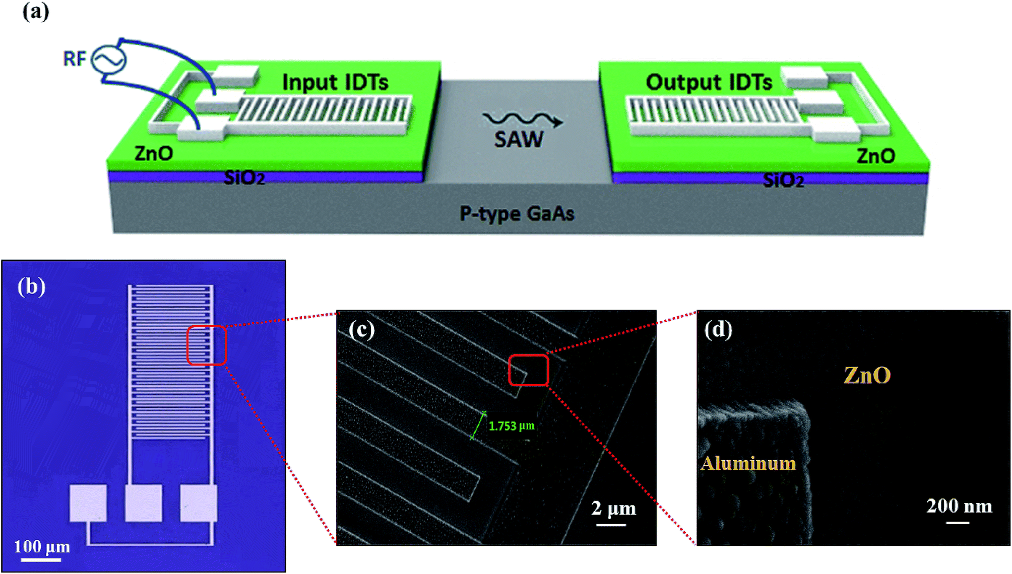 | ||
| Fig. 1 Structure demonstration of the SAW device: (a) three-dimensional schematic view of the input and output IDT device deposited on a ZnO/SiO2 island on a highly doped p-type GaAs substrate. With the applied radio frequency signals on input IDTs, a SAW is generated and propagated from left to right on the surface of the GaAs substrate. (b) Optical microscope image of the device, showing the comb structure of the IDT fingers (top half) and three contact pads (bottom half) designed for probe station testing equipment. (c) Scanning electron microscope (SEM) image of the amplified view of IDT fingers. (d) High-resolution SEM image showing the surface morphology of the aluminum IDT finger and the c-axis oriented ZnO layer. | ||
The metal IDTs in our design are in the conventional single-finger form. The spacing between IDT fingers is the same as the finger width. In this case, according to the concept and theory of SAWs,18,28 the wavelength of SAWs is equal to four times the width of an IDT finger when the SAW is launched with the fundamental frequency of the IDT. As the propagating speed of the SAW in each specific material is known, the center frequency of the SAW can be determined as well. According to the literature, the SAW velocity in ZnO varies from 2600 m s−1 to 5000 m s−1 depending on the thickness and structure,15,29,30 and the SAW velocity in GaAs is approximately 2700 m s−1 to 2900 m s−1.31,32 In our design, since the SAW completely propagates on the surface of the p-type GaAs substrate along the delay line (without the ZnO film), the center frequency is determined by the IDT finger width and the SAW velocity in GaAs.
The photos taken with an optical microscope (Fig. 1(b)) and scanning electron microscope (Fig. 1(c) and (d)) present a clear fabrication outcome and accurate dimensions. The metal IDT fingers are well shaped. The surface of the ZnO film is clean and smooth as needed for generating SAWs successfully.
2.2 Sample fabrication
The 3-dimensional schematic diagram in Fig. 2(a) shows the detailed fabrication process of the ZnO-enhanced SAW structure. The process started with using a highly doped p-type (100) GaAs wafer as the substrate. The doping concentration of the substrate ranges from 5 × 1018 cm−3 to 3 × 1019 cm−3. For the first stage of sample preparation, a standard cleaning process was applied with acetone and isopropyl alcohol (IPA), as well as using a sonicator if necessary. Next, we used the PECVD method with an optimized recipe to deposit SiO2 layers on top of the GaAs substrate at a rate of 120 nm per minute. Then we used a RF magnetron sputtering system to deposit a thin layer of ZnO on top of the SiO2 buffer layer.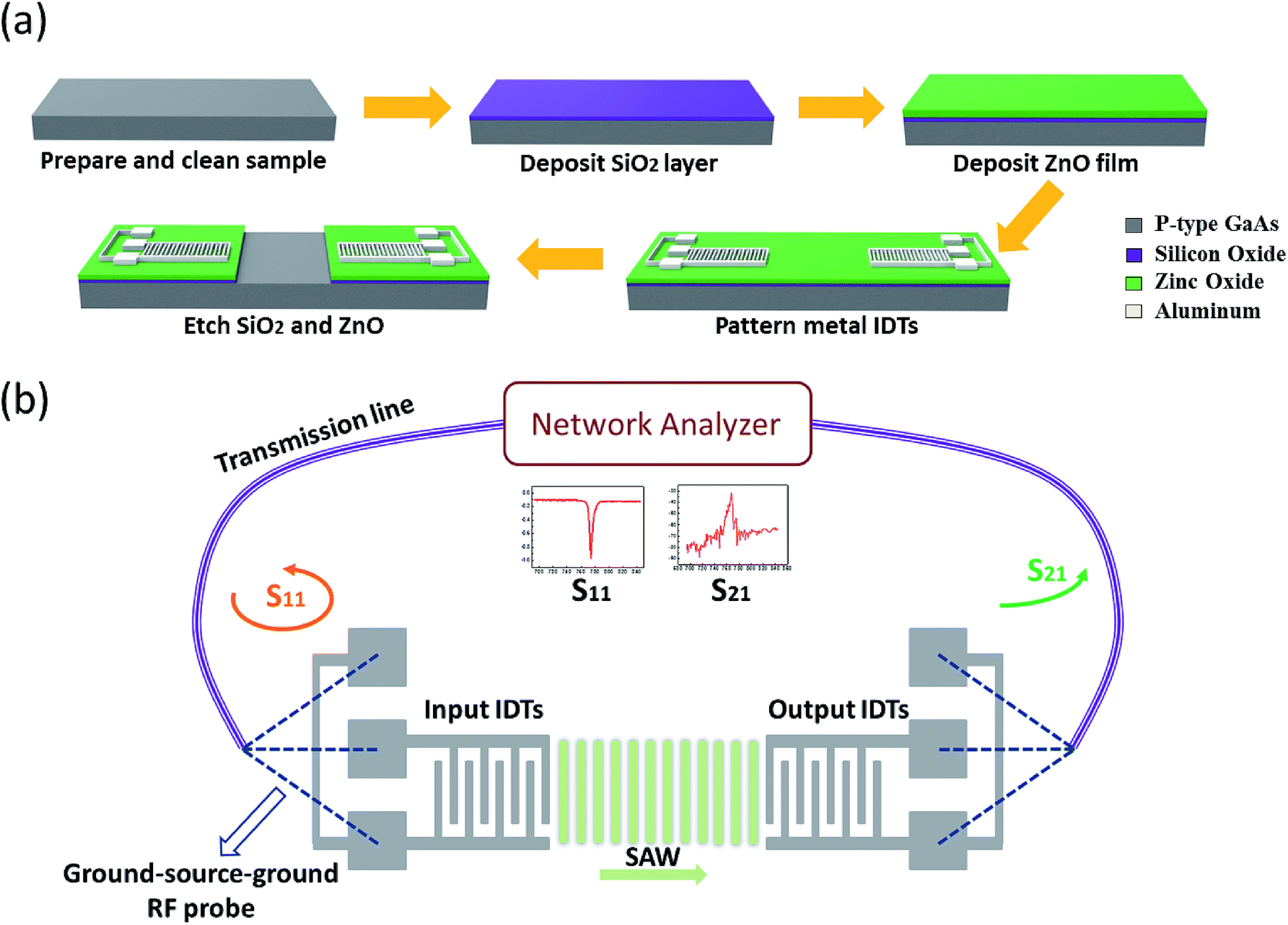 | ||
| Fig. 2 (a) Fabrication process flow of the device: deposition of the SiO2 intermediate layer and ZnO thin layer, e-beam lithography and e-beam metal evaporation for aluminum IDTs, and etching of SiO2 and ZnO to open a window for the GaAs surface in the center. (b) Testing equipment: using RF probes and transmission line cables to connect the fabricated IDT device to a network analyzer to measure the transmission (S21) and reflection (S11) properties of SAWs. | ||
For transferring the pattern, first a PMMA (A4) photoresist was spin-coated on top of the ZnO layer with a speed of 3000 rpm for two minutes. The sample was baked on a hot plate at a temperature of 180 °C for 2 minutes. Then this spin-coating and heating process was repeated once more. Next, the process of e-beam exposure was conducted with a Raith Voyager Electron Beam Lithography (EBL) system to transfer the pattern onto the surface. The patterned photoresist was developed in methyl isobutyl ketone (MIBK) solution for 90 seconds. Then metallization with an e-beam evaporator was used to form the aluminum IDT electrode fingers. After that, the unwanted photoresist structure was lifted off with acetone for 20 minutes to get the IDT electrode fingers on top of ZnO. The next step was to spin-coat another layer of the photoresist on top of the sample using the same method described previously. The process of e-beam exposure was conducted again with the Raith Voyager EBL system to transfer the second pattern on the top center of the sample, which was used to etch ZnO/SiO2 and open a window as shown in Fig. 2(a). Afterwards, the photoresist was developed in MIBK solution for 90 seconds. Then the wet etching method and the reactive ion etcher (RIE) method were used to eliminate the patterned area of the ZnO layer and SiO2 layer, respectively, to create the window which has p-type GaAs exposed on the surface of the sample. The last step was to lift off the unwanted photoresist with acetone for 15 minutes to obtain the final structure of the device.
2.3 Sample characterization and measurement
The fabrication outcomes were characterized by using an optical microscope and scanning electron microscope (SEM) to make sure that the device structure and dimensions, thickness of layers, and surface morphology are achieved as designed. X-ray diffraction measurements were conducted on the surface of the ZnO layer to verify the quality of RF sputtering deposition and to confirm the orientation of the deposited ZnO film.Then, the sample with IDT devices was placed on a probe station. Both input IDTs and output IDTs are connected with an RF probe, separately. Each RF probe has three pins, which are ground–source–ground respectively. Thus we have three corresponding square contact pads on our IDT design, as shown in Fig. 2(b). Next, the two RF probes were connected to the two ports of a network analyzer via two transmission line cables. The network analyzer was used to apply scanning high frequency RF signals ranging from 50 MHz to 2 GHz between IDT fingers, and to measure the transmission and reflection characteristics (S-parameter) of SAWs. Here, we focused on the measurement of S21 and S11. The transmission coefficient S21 refers to how much power is transmitted from input IDTs to output IDTs through the SAW. The reflection coefficient S11 refers to how much power is reflected back from the input IDTs. As for the case of our single-finger IDT design (as shown in Fig. 1), when there is no SAW generated or weak SAW propagation, the S21 indicates a big transmission loss and the S11 is close to 0 dB, suggesting that most of the power cannot be transmitted to the output. On the other hand, when a strong SAW is generated and propagated from the input to the output, the S21 shows a peak at the center frequency with a bandwidth, and the S11 has a dip in the same frequency range, as shown in the insets of Fig. 2(b).
3 Results and discussion
3.1 Quality of the ZnO layer
Before building devices following the fabrication process described above, it is essential to obtain a high quality deposition of ZnO layer. For a stronger piezoelectric effect, ZnO needs to be deposited with a high quality c-plane facing up when using the RF sputtering method, as SAWs cannot be generated and transmitted strongly on a low quality ZnO surface. The recipe of the RF magnetron sputtering system includes many parameters such as the plate temperature, gas flow ratio, VAT pressure, time length, pre-sputter and sputter power, and each has its impact on the deposition results.Fig. 3(a) and (b) exhibit SEM pictures showing the top surface topography of the deposited ZnO layers. Both figures have the same magnification and thus good to compare. The two samples are ZnO layers deposited using different recipes in the RF magnetron sputtering system on two pieces of highly doped p-type GaAs substrates cut from the same wafer. Fig. 3(a) shows a low quality ZnO deposition with a very rough and cracked surface, making it difficult to pattern and deposit metal IDTs, and thus cannot be used to generate SAWs. After modifying parameters in the recipe, a high quality deposited ZnO layer is achieved with a smooth and clean surface and small ZnO grain size, as shown in Fig. 3(b).
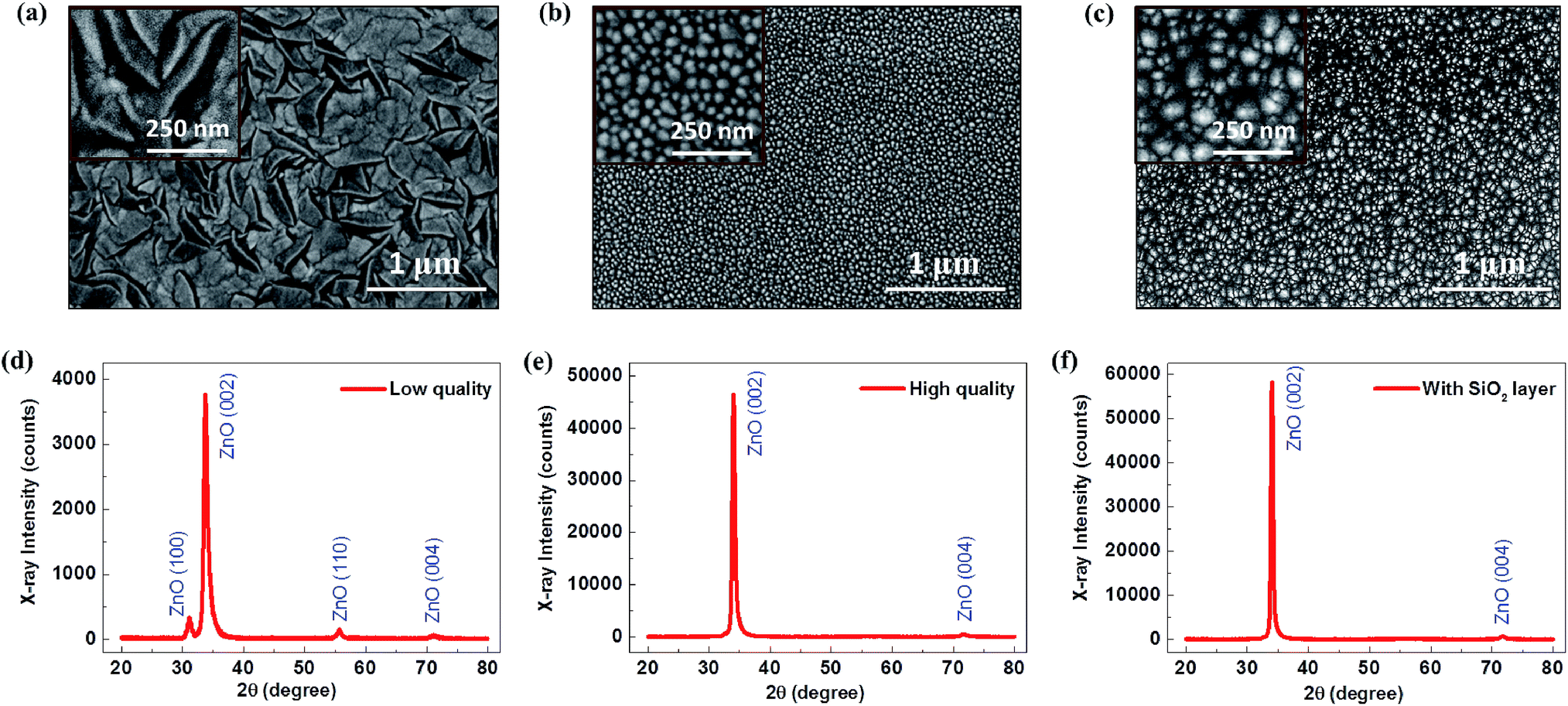 | ||
| Fig. 3 Quality of ZnO layer deposition using the RF magnetron sputtering method: (a) top surface SEM image and (d) X-ray diffraction pattern of the ZnO film (thickness: 1400 nm) grown on the p-type GaAs substrate resulting in a low quality outcome. The sputtering conditions of this sample are: P = 350 W, T = 130 °C, Ar/O2 = 69 sccm/0 sccm, pressure = 17 mTorr, and t = 2 hour. (b) Top surface SEM image and (e) X-ray diffraction pattern of a high-quality c-axis oriented ZnO film (thickness: 1100 nm) grown on the p-type GaAs substrate. The sputtering conditions of this sample are: P = 400 W, T = 250 °C, Ar/O2 = 50 sccm/11 sccm, pressure = 8 mTorr, and t = 2 hour. (c) Top surface SEM image and (f) X-ray diffraction pattern of a high-quality c-axis oriented ZnO film (thickness: 1100 nm) with the same sputtering conditions as (b and e), but grown on a sample with an additional SiO2 buffer layer. The insets on the top left in (a–c) show the amplified view of each corresponding SEM image. | ||
The crystalline structure of the two deposited ZnO films using different RF sputtering recipes are also characterized using θ–2θ X-ray diffraction (XRD). Fig. 3(d) and (e) show XRD plots of low quality and high quality ZnO films, respectively. Upon comparing the two plots, it is clear that the high quality ZnO film has a much higher intensity of the (002) peak and a smaller number of off-oriented crystals. Also, the built-in lattice strain reduced from 1.369% to 0.512%, and the full width at half maximum (FWHM) value of the (002) XRD reflection line reduced from 0.639 degree to 0.392 degree. These results prove that, with the modified recipe, a highly textured and highly c-axis oriented ZnO layer can be grown on the p-type GaAs substrate.
Fig. 3(c) and (f) show the outcome of the ZnO film deposited on a sample with an added SiO2 buffer layer using the same RF sputtering recipe for high-quality ZnO. According to the SEM image (Fig. 3(c)), the ZnO film exhibits a more visible hexagonal crystal structure with an increased grain size. Additionally, by comparing the XRD plots in Fig. 3(e) and (f), one can see that the higher intensity of the (002) peak is achieved with the help of the SiO2 buffer layer. Also, the built-in lattice strain reduced from 0.512% to 0.437%, and the FWHM value of the (002) XRD reflection line reduced from 0.392 degree to 0.325 degree. These results confirm that a better crystal orientation of high-quality ZnO along the c-axis direction can be formed with a SiO2 buffer layer added between the ZnO film and p-type GaAs substrate.
3.2 Enhancement of SAWs by ZnO
Next, metal IDTs were deposited on top of the high quality c-axis oriented ZnO layer. To verify that the ZnO film is able to enhance the SAW propagation on the p-type GaAs surface, we tested different samples. One was an IDT structure deposited on the p-type GaAs substrate with an added ZnO layer, and the other one was without the ZnO layer. The comparison result of the transmission characteristics (S-parameter S21) of SAWs measured by using a network analyzer is shown in Fig. 4(d).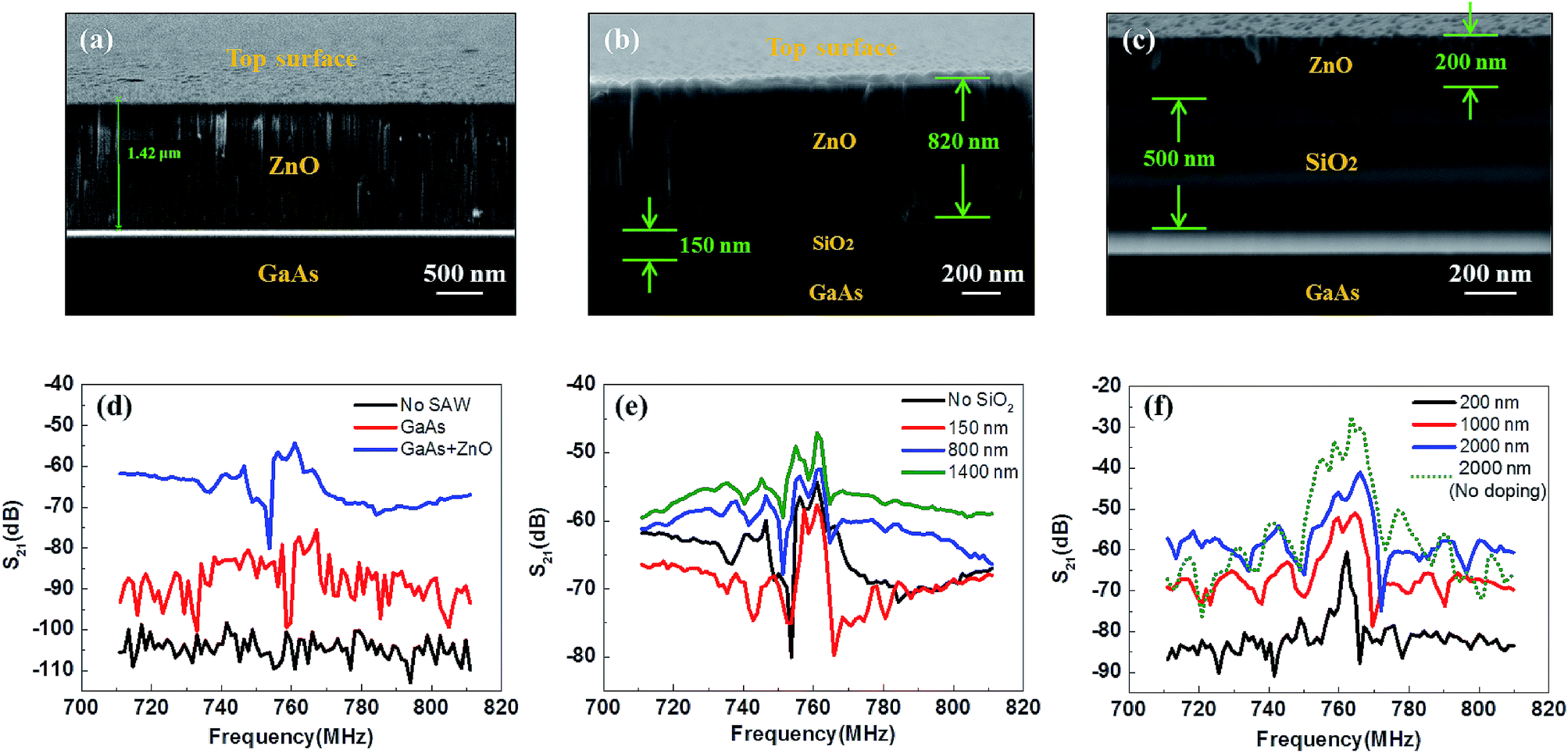 | ||
| Fig. 4 Experimental results on samples with different layer structures: (a) SEM image of the cross-sectional view of the ZnO layer deposited on top of the p-type GaAs substrate without a buffer layer of SiO2. (b) SEM image of the cross-sectional view of a sample that has a ZnO/SiO2/GaAs layer structure. (c) SEM image of the cross-sectional view of a sample that has a thicker SiO2 buffer layer and thinner ZnO film. (d) Comparison of the transmission property S21 of SAWs generated by IDTs deposited on the p-type GaAs substrate with and without an added ZnO layer. (e) Comparison of the transmission performance of SAWs generated on samples with an intermediate SiO2 layer of different thicknesses. (f) The three solid curves are comparison results showing the dependence of SAW enhancement on the thickness of ZnO films. The green dotted curve is the result from a sample fabricated on an undoped GaAs substrate. All experimental and test results presented in this section are conducted on single-finger IDTs with a finger width of 0.9 μm. The SAW delay line between each pair of input IDTs and output IDTs has the same distance (800 μm) and [011] direction. | ||
Fig. 4(a) shows the cross sectional view of the ZnO layer deposited on the p-type GaAs substrate. The lower black area is the GaAs substrate. The upper grey area shows the top surface of the ZnO layer, which is the same as the high quality c-plane ZnO shown in Fig. 3(b). The middle area is the fractured surface of the ZnO layer. The view of the fractured surface shows a dense and columnar structure, which once again verifies the high quality of the c-axis oriented crystalline structure of the ZnO film. The green line and number are used to measure and indicate the thickness of the ZnO layer, which is 1.42 μm in this sample.
In Fig. 4(d), the red line is the transmission coefficient S21 of the SAW generated by IDTs put on the surface of p-type GaAs. The blue line shows the result of the sample that has a ZnO layer added on top of p-type GaAs. The black line shows the result when there is no SAW propagation. According to the concept introduced in Section 2.1, the center frequency of the SAW in this case is determined by four times the IDT finger width (3.6 μm) and the SAW velocity in GaAs (∼2800 m s−1), which gives fSAW ∼ 770 MHz by calculation. The measurement result shown in Fig. 4(d) is consistent with this theoretical expectation. By comparison, the peak value of S21 at the center frequency of the SAW increased from −100 dB to −75 dB on p-type GaAs before and after generating SAWs. This result shows the very weak piezoelectric coupling effect of the highly p-doped GaAs substrate. Then with the enhancement brought about by the added ZnO layer, the peak value of S21 increased further to −55 dB. According to this result, the insertion loss becomes smaller, indicating that a stronger SAW is generated and propagated on the p-type GaAs surface as a result of the added ZnO film. On the other hand, not only the peak value, the S21 in the whole measurement range around the center frequency increased. This can be explained by the existence of higher-order harmonics and other pseudo-surface waves and shear waves,30,33 which together contribute to the frequency response in the whole measurement range, especially for a basic IDT design without reflectors.21 In other words, when the piezoelectric coupling effect is enhanced, not only the SAW at the center frequency gets stronger, but also a wide range of frequency response increases, as seen in the literature.17,21,30,33 This wide-range increase of frequency response is also observed in Fig. 4(e) and (f), which is discussed in Section 3.3 and Section 3.4, respectively. The measurement result presented in this section proves that a strong piezoelectric material such as ZnO can be used to improve the performance of SAWs on highly doped p-type GaAs.
3.3 Intermediate layer of SiO2
The next step was to use a SiO2 buffer layer to further improve the design. According to the literature, an intermediate layer of SiO2 deposited between GaAs and ZnO will effectively mask the crystalline surface of GaAs and thus allow good adherence and better texture quality of the ZnO deposition.20,21 A higher quality of the ZnO film will lead to enhanced piezoelectric coupling and improved SAW performance. To verify whether an intermediate layer of SiO2 is able to enhance the SAW, multiple samples with an added SiO2 layer were fabricated and tested. A comparison of the transmission performance of SAWs is presented in Fig. 4(e).During the fabrication of this design, first we used the PECVD method to deposit SiO2 layers with varied thicknesses on different p-type GaAs substrates. Then ZnO films were deposited with the same thickness (800 nm) on top of SiO2 on those samples using the RF magnetron sputtering method. Fig. 4(b) shows the SEM picture showing the cross-sectional view of a thin SiO2 layer added as an intermediate layer between ZnO and GaAs. The material names in yellow color in Fig. 4(b) indicate different layers from bottom to top. The green lines with arrows and numbers are used to measure and indicate the thicknesses of the ZnO layer (820 nm) and SiO2 layer (150 nm). Fig. 4(c) shows the cross-sectional view of a thicker SiO2 layer (500 nm) embedded as an intermediate layer between a thinner ZnO film (200 nm) and p-type GaAs substrate.
From results shown in Fig. 4(e), compared to the sample without an intermediate SiO2 layer (black line), a thin layer of SiO2 (150 nm, red line) results in a higher insertion loss, which is a sign of reduced performance of SAWs. The peak value of S21 at the center frequency of the SAW decreases from −54 dB to −57 dB, as well as the values in the rest of the frequency range. Then, with the increase of SiO2 thickness, the peak value at the center frequency of the SAW on the sample with an 800 nm SiO2 layer (blue line) increases to −52 dB, which is a little bit higher than the one without SiO2 (black line). After continuously increasing the thickness of the SiO2 layer to 1400 nm (green line), the values of S21 in the whole frequency range appear clearly higher than the one without the SiO2 layer. Both the peak value at the center frequency (−47 dB) and the bandwidth are improved, which proves the enhancement of SAW transmission performance.
3.4 Thickness of ZnO
On the other hand, in order to study the dependence of SAW enhancement on the thickness of the ZnO film, we fabricated and tested samples with different thicknesses of ZnO layers at 200 nm, 1000 nm and 2000 nm. We used the same recipe of RF magnetron sputtering and thus the orientation, quality and deposition rate of ZnO films were consistent for all samples. By setting different deposition time, the thickness of achieved ZnO films was varied. Besides the thickness of ZnO films, other parameters of the structure and dimensions (as shown in Fig. 4(c)) are the same for all samples as well. Measurement results of the transmission coefficient S21 of the different samples are shown in Fig. 4(f).According to the comparison, both the peak value of S21 (from −60 dB to −51 dB) at the center frequency and the bandwidth of the SAW improve when increasing the thickness of the ZnO film from 200 nm (black line) to 1000 nm (red line). Then as the thickness of the ZnO film continues to increase to 2000 nm (blue line), the peak value of S21 increases further to −41 dB while the bandwidth does not increase much. This result shows a trend that a thicker ZnO film provides bigger enhancement of the SAW on the p-type GaAs substrate.
Additionally, in order to show the attenuation of the propagating SAW due to the free carriers doped in the GaAs substrate, we fabricated a SAW delay line on an undoped GaAs substrate with the same layer structure and IDT design, as well as all other parameters. The test result is plotted in Fig. 4(f) as a dotted green line. By comparing it to the solid blue line (both samples have a 2000 nm ZnO film), a difference of 14 dB in the peak value of S21 (from −41 dB to −27 dB) at the center frequency is found, while the bandwidths are close to each other. This SAW attenuation caused by the interaction of the piezoelectric field with the free carriers in the doped GaAs substrate is consistent with the expectation.
3.5 Dimensions of IDTs
As discussed in Section 2.1, the center frequency of the SAW is determined by the IDT dimensions and the SAW velocity in a specific material. When the material (GaAs) is known, the center frequency changes with the IDT dimensions. In order to observe this property in our design and also to find out the dependence of SAW performance on frequency, the study and comparison of IDTs with different sizes are given in this section. We fabricated two pairs of SAW devices with different IDT finger widths (0.9 μm and 2.3 μm) on the same ZnO/SiO2/GaAs sample. Photos taken with an optical microscope shown in Fig. 5(a) and (e) are used to verify the outcomes of fabrication and the accuracy of IDT dimensions. The device structures of both IDT finger widths are well fabricated and their sizes are as desired.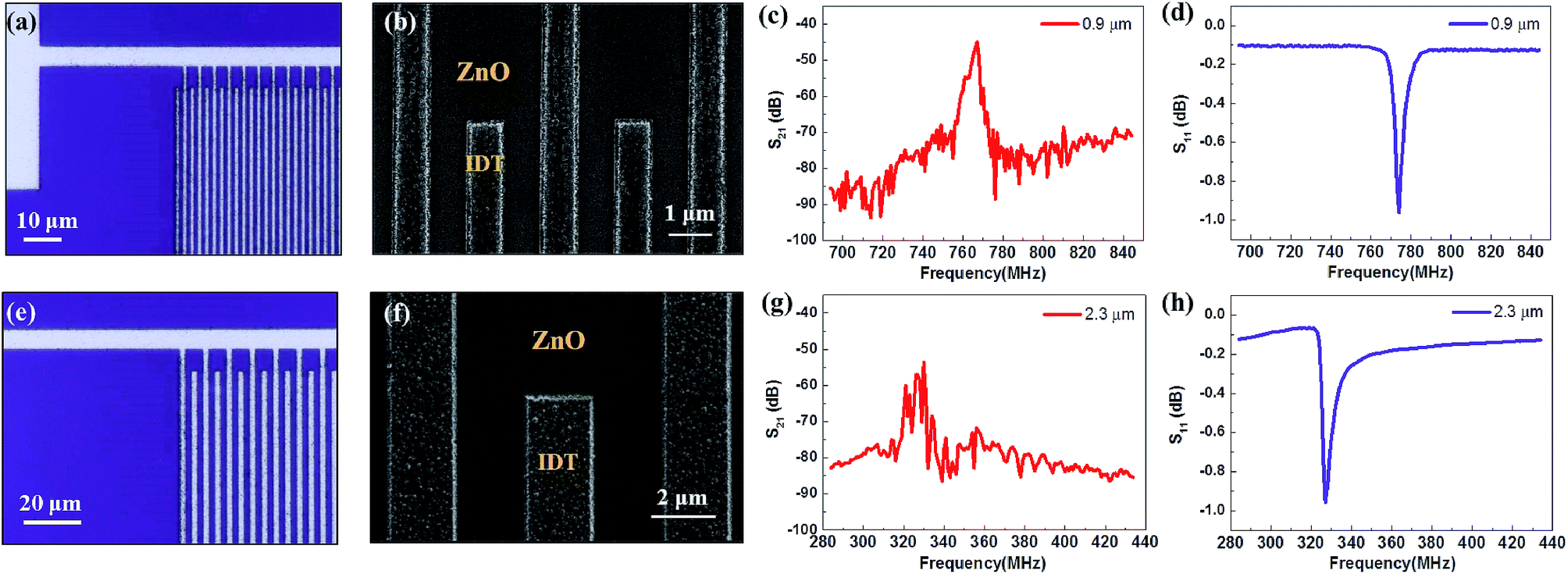 | ||
| Fig. 5 Experimental results of devices with different IDT dimensions: (a) optical microscope image and (b) SEM image of the top surface view of IDT fingers placed on the ZnO film with a finger width of 0.9 μm. (c) Transmission characteristic S21 and (d) reflection characteristic S11 of SAWs generated by applied radio frequency AC voltage on 0.9 μm IDTs. (e–h) Corresponding results for the device with IDT fingers of 2.3 μm width. Both pairs of IDTs were fabricated on the same sample. They were designed to have the same acoustic impedance that can be matched as well as possible to the impedance of the network analyzer and the transmission line, which is close to 50 Ω. The delay line between each pair of input IDTs and output IDTs has the same distance (1200 μm) and [011] direction. | ||
Fig. 5(b) and (f) show photos taken with a SEM to give a magnified view of IDTs deposited on the ZnO surface. It is clear that the metal IDT fingers are well shaped and deposited during fabrication. The width of IDTs and the distance between two IDTs are 0.9 μm and 2.3 μm respectively as designed. The metal surface is a little rough due to the quality of chamber vacuum during the e-beam evaporation process. The ZnO surface, however, is smooth and clean as needed.
Curves plotted in Fig. 5(c) and (d) show the transmission properties (S-parameter S21) and reflection properties (S-parameter S11) of the SAW generated through the 0.9 μm-width IDT device, respectively. The x-axis refers to the radio frequency range, and the y-axis refers to transmission loss and reflection loss in the unit of dB. Similarly, Fig. 5(g) and (h) show the plots of S21 and S11 of the SAW generated by IDTs with a finger width of 2.3 μm. From these plots, we can see that the SAWs are successfully generated and transmitted along the highly doped p-type GaAs surface in both cases. For the sample with the 0.9 μm IDT finger, the center frequency of the SAW is 767 MHz with an insertion loss (S21) of −44.9 dB and the value of S11 is −0.96 dB. For the sample with the 2.3 μm IDT finger, the center frequency of the SAW changed to 326 MHz. The transmission peak value of S21 decreased to −57.1 dB and the reflection coefficient S11 dip changed to −0.95 dB. This center frequency shift with the change of IDT sizes (from 0.9 μm to 2.3 μm) is consistent with the theory that a smaller width of IDT fingers leads to a proportionally higher center frequency of SAW resonance in a specific piezoelectric material. It shows the capability of our design in propagating SAWs with different frequencies on highly doped p-type GaAs. In addition, by comparison between the two cases, we can see that the SAW with a higher frequency has better transmission performance on the p-type GaAs surface with the help of the ZnO/SiO2 island design.
4 Modelling and simulation
To further verify that the ZnO thin film in our designed structure is capable of enhancing the piezoelectric coupling effect on highly doped p-type GaAs and generating stronger SAWs, we used commercial simulation software COMSOL Multiphysics to do finite element analysis.Fig. 6(b) shows the SAW generated on the ZnO substrate that has a strong piezoelectric coupling coefficient. On top of the ZnO layer, three pairs of IDTs made of aluminum are placed and used to generate periodically distributed piezoelectric fields. Among them, IDT no. 2, no. 4 and no. 6 are grounded, and IDT no. 1, no. 3 and no. 5 are applied to AC input voltage that is expressed in the following equation:
| Vin = V0 × sin(2π × f0 × t) | (1) |
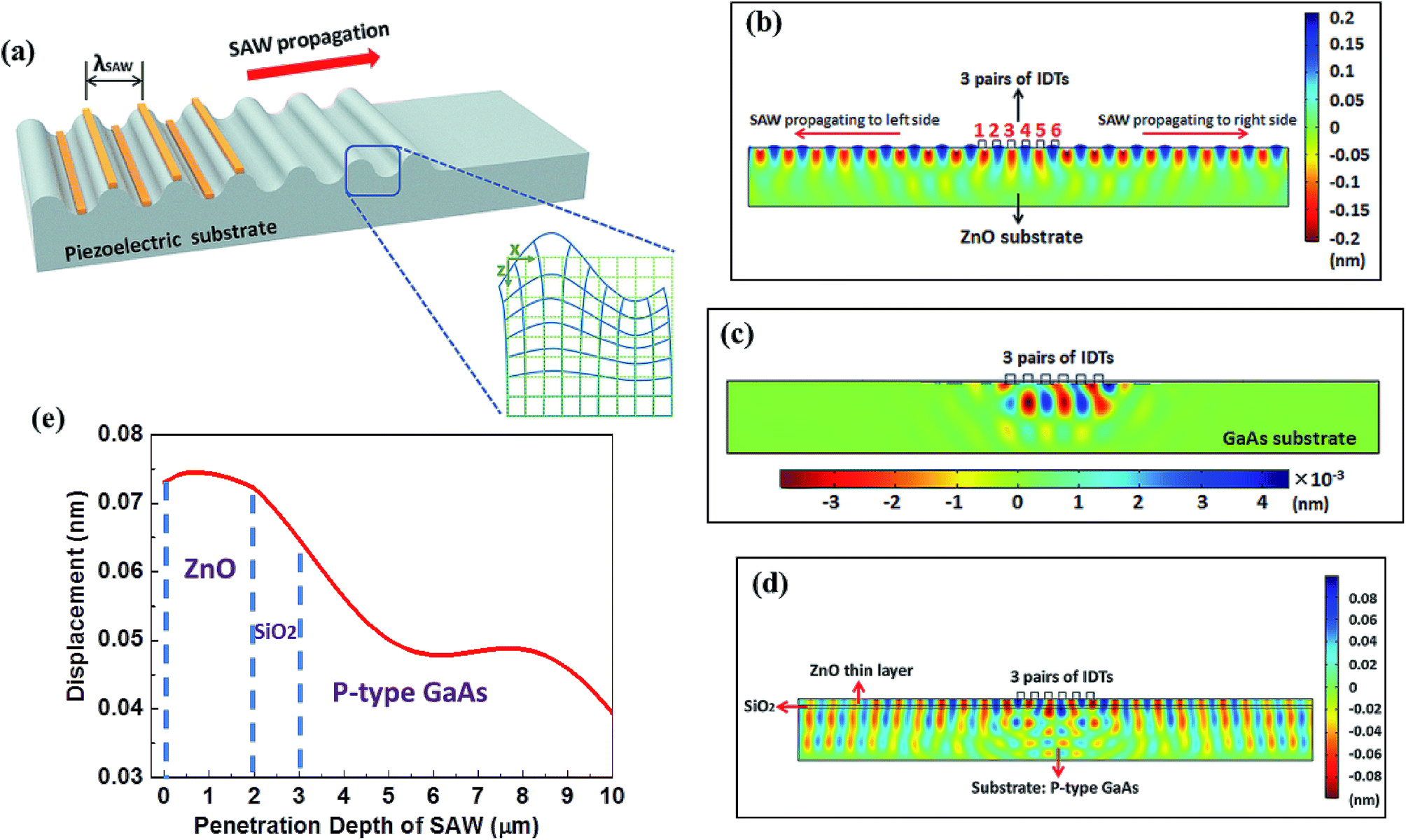 | ||
| Fig. 6 Simulation of SAW enhancement for the ZnO/SiO2/GaAs structure: (a) concept and mechanism of SAW propagation along the delay line and leading to surface deformations. The inset at the right corner shows the concept in a microscopic view that the crystal lattice is shifted up and down under the applied periodical piezoelectric potential and electric field. This, on the macroscopic scale, results in a periodical surface deformation and a propagating acoustic wave along the surface. The extent of surface displacement is in direct proportion to the built-in piezoelectric potential and electric field. Simulation results of surface deformations induced by SAWs that are generated and propagated on the (b) ZnO substrate, (c) GaAs substrate, and (d) ZnO thin film and SiO2 buffer layer placed on top of the GaAs substrate. (e) Simulation result to show the loss of SAW energy as the SAW penetrates from ZnO/SiO2 into the GaAs substrate. | ||
The results in Fig. 6(b) indicate the amount of surface deformation induced by SAWs. The separated areas in either blue color or red color suggest that the surface is shifted up and down, the same as the 3D schematic model shown in Fig. 6(a).
Next, GaAs is chosen as the substrate material. The (100) GaAs substrate is p-type doped with a doping concentration of 5 × 1018 cm−3. The IDTs are oriented along the [011] propagation direction. The piezoelectric coupling coefficient of GaAs is much smaller compared to those of commonly used piezoelectric materials.13,14 As a result, the generated SAW is weak, as shown in Fig. 6(c).
In Fig. 6(c), the structure and dimensions of the substrate and IDTs as well as the applied AC voltage are completely the same as those designed in Fig. 6(b). The only difference is that the substrate material was changed from ZnO to GaAs. By comparing the two simulation results at the same instant of time (t = 34.6 ns), we can see smaller surface displacement in GaAs than that in ZnO. The maximum amount of displacement (in the vertical direction) on the ZnO substrate is about 0.2 nm. For the GaAs substrate, however, the maximum amount of displacement is only around 0.004 nm. This verifies that GaAs has a much weaker piezoelectric coupling effect than ZnO. Additionally, according to the SAW velocity used in simulation (also discussed in Section 2.1), the SAW should propagate from the IDT to the end (distance: 85 μm) within 31 ns. As shown in Fig. 6(b), the SAW reaches the right and left ends of the structure when t = 34.6 ns as expected. However, for the GaAs substrate in Fig. 6(c), the SAW cannot visibly propagate that far at the same instant of time.
As discussed above, to enhance the piezoelectric coupling for p-type GaAs, a thin film of ZnO (2 μm) and a buffer layer of SiO2 (1 μm) are placed on top of the GaAs substrate. The IDTs (width: 2.3 μm) are then placed on top of the ZnO layer. The [011] propagation direction of the SAW and other corresponding parameters are the same as those used in Fig. 6(b) and (c). Fig. 6(d) shows the simulation result of the new structure, which is captured at the same moment t = 34.6 ns. According to this new simulation result, the generated SAW becomes much stronger when compared with the one shown in Fig. 6(c). The maximum amount of displacement in GaAs increases fifteen times from 0.004 nm to 0.06 nm. In addition, the SAW is now able to propagate from IDTs to the ends of the right side and left side of the substrate surface. The curve in Fig. 6(e) is extracted and plotted from the simulation result of Fig. 6(d), showing the displacement amplitude induced by the SAW field along the penetration depth of the SAW in the vertical direction. It is used to indicate the energy loss when the SAW penetrates from ZnO/SiO2 into GaAs. As shown in Fig. 6(e), location x = 0 refers to the top surface of the ZnO film, and then followed by the SiO2 layer (2 < x < 3) and GaAs substrate (x > 3). It can be clearly seen that, even though an attenuation of the SAW field exists in the ZnO/SiO2 region, the displacement amplitude in GaAs (0.05–0.06 nm) within a depth of several microns is much higher than the amount shown in Fig. 6(c). It verifies the SAW enhancement in p-type GaAs although some of the SAW energy was lost in the ZnO/SiO2 region. These simulation results are consistent with the expected results described in theory and are identical to the experimental results we demonstrated in this paper, proving the function of our designed structure.
5 Conclusion
In this work, we studied and demonstrated a method of using a strong piezoelectric material ZnO with the RF magnetron sputtering deposition technique to enhance the piezoelectric coupling effect on the surface of a highly doped p-type GaAs substrate. Our presented technique has been proven successful in forming high quality c-axis oriented ZnO films and generating strongly enhanced SAWs that can propagate on p-type GaAs. Both the experimental results of the fabricated devices and the simulations verified this enhancement. Furthermore, we built and tested samples with intermediate SiO2 layers and found that an added SiO2 layer with an appropriate thickness can further improve the performance of SAWs. We also investigated the dependence of SAW properties on various factors such as the thickness of ZnO films and the sizes of IDT fingers. This work paves the way for further investigations of acousto-electric properties of highly doped semiconductor materials and enables wider utilization of those materials in acoustic, electrical and optical applications.Conflicts of interest
There are no conflicts to declare.Acknowledgements
The research was partially supported by the U.S. Department of Energy (DOE) HEP STTR grant under award number DE-SC0017831. We gratefully appreciate the support from Dr Rolland Johnson and Muplus, Inc., and the nanofab facilities provided at the National Institute of Standards and Technology (NIST) and George Washington University (GWU). We also thank Dr Andrei Afanasev for the enlightening discussion and advice during the work.References
- S. Zhang, S. Lin, X. Li, X. Liu, H. Wu, W. Xu, P. Wang, Z. Wu, H. Zhong and Z. Xu, Nanoscale, 2016, 8, 226–232 RSC.
- X. Li, S. Lin, X. Lin, Z. Xu, P. Wang, S. Zhang, H. Zhong, W. Xu, Z. Wu and W. Fang, Opt. Express, 2016, 24, 134–145 CrossRef CAS PubMed.
- B. Dong, S. Guo, A. Afanasev and M. Zaghloul, 2016, IEEE 43rd Photovoltaic Specialists Conference, PVSC, 2016, pp. 2087–2090 Search PubMed.
- S. Zhang, M. Poelker, M. L. Stutzman, X. Peng and J. Zou, Negative Electron Affinity Gallium Arsenide Photocathodes Based on Optically Resonant Nanostructure, Technical report, Thomas Jefferson National Accelerator Facility, Newport news, VA (United States), 2018 Search PubMed.
- C. Rocke, S. Zimmermann, A. Wixforth, J. Kotthaus, G. Böhm and G. Weimann, Phys. Rev. Lett., 1997, 78, 4099 CrossRef CAS.
- M. M. de Lima Jr and P. V. Santos, Rep. Prog. Phys., 2005, 68, 1639 CrossRef.
- A. Violante, K. Cohen, S. Lazić, R. Hey, R. Rapaport and P. V. Santos, New J. Phys., 2014, 16, 033035 CrossRef.
- B. Dong, S. Guo and M. Zaghloul, URSI Asia-Pacific Radio Science Conference, URSI AP-RASC, 2016, pp. 1921–1924 Search PubMed.
- S. Büyükköse, A. Hernandez-Minguez, B. Vratzov, C. Somaschini, L. Geelhaar, H. Riechert, W. G. van der Wiel and P. Santos, Nanotechnology, 2014, 25, 135204 CrossRef PubMed.
- B. Dong, M. Zaghluol, A. Afanasev and R. P. Johnson, Proc. IPAC2018, Vancouver, BC, Canada, 2018 Search PubMed.
- A. Hernández-Mínguez, M. Möller, C. Pfüller, S. Breuer, O. Brandt, M. de Lima, A. García-Cristóbal, A. Cantarero, L. Geelhaar, H. Riechert, et al., MRS Online Proceedings Library Archive, 2012, p. 1408 Search PubMed.
- S. Hermelin, S. Takada, M. Yamamoto, S. Tarucha, A. D. Wieck, L. Saminadayar, C. Bäuerle and T. Meunier, J. Appl. Phys., 2013, 113, 136508 CrossRef.
- Y. Kim, W. D. Hunt, F. S. Hickernell and R. J. Higgins, J. Appl. Phys., 1994, 75, 7299–7303 CrossRef CAS.
- E. D. Nysten, Y. H. Huo, H. Yu, G. F. Song, A. Rastelli and H. J. Krenner, J. Phys. D: Appl. Phys., 2017, 50, 43LT01 CrossRef.
- A. Hernández-Mínguez, Y. Liou and P. Santos, J. Phys. D: Appl. Phys., 2018, 51, 383001 CrossRef.
- J. Rudolph, R. Hey and P. Santos, Phys. Rev. Lett., 2007, 99, 047602 CrossRef.
- M. Yuan, C. Hubert, S. Rauwerdink, A. Tahraoui, B. van Someren, K. Biermann and P. Santos, J. Phys. D: Appl. Phys., 2017, 50, 484004 CrossRef.
- C. C. Ruppel and T. A. Fjeldly, Advances in surface acoustic wave technology, systems and applications, World scientific, 2001, vol. 2 Search PubMed.
- Y. Kim, W. D. Hunt, F. S. Hickernell, R. J. Higgins and C.-K. Jen, IEEE Trans. Ultrason. Eng., 1995, 42, 351–361 Search PubMed.
- K.-H. Bang, D.-K. Hwang and J.-M. Myoung, Appl. Surf. Sci., 2003, 207, 359–364 CrossRef CAS.
- W.-C. Shih and M.-S. Wu, J. Cryst. Growth, 1994, 137, 319–325 CrossRef CAS.
- X. Du, Y. Fu, S. Tan, J. Luo, A. Flewitt, S. Maeng, S. Kim, Y. Choi, D. Lee and N. Park, et al. , J. Phys.: Conf. Ser., 2007, 012035 CrossRef.
- M. Gillinger, K. Shaposhnikov, T. Knobloch, M. Schneider, M. Kaltenbacher and U. Schmid, Appl. Phys. Lett., 2016, 108, 231601 CrossRef.
- G. McHale, M. K. Banerjee, M. Newton and V. Krylov, Phys. Rev. B: Condens. Matter Mater. Phys., 1999, 59, 8262 CrossRef CAS.
- X. Du, Y. Q. Fu, S. Tan, J. Luo, A. Flewitt, W. Milne, D.-S. Lee, N.-M. Park, J. Park and Y. Choi, et al. , Appl. Phys. Lett., 2008, 93, 094105 CrossRef.
- A. Wixforth, J. Scriba, M. Wassermeier, J. Kotthaus, G. Weimann and W. Schlapp, Phys. Rev. B: Condens. Matter Mater. Phys., 1989, 40, 7874 CrossRef CAS PubMed.
- M. Chang, C. Lee, P. Asbeck, R. Vahrenkamp and C. Kirkpatrick, Appl. Phys. Lett., 1984, 45, 279–281 CrossRef CAS.
- V. M. Yakovenko, Phys. B, 2012, 407, 1969–1972 CrossRef CAS.
- J. X. Ding, D. Chen, L. Du and G. M. Liu, Applied Mechanics and Materials, 2012, pp. 1894–1898 Search PubMed.
- E. B. Magnusson, B. H. Williams, R. Manenti, M.-S. Nam, A. Nersisyan, M. J. Peterer, A. Ardavan and P. J. Leek, Appl. Phys. Lett., 2015, 106, 063509 CrossRef.
- C. K. Campbell, Proc. IEEE, 1989, 77, 1453–1484 CrossRef.
- C. Campbell, Surface acoustic wave devices and their signal processing applications, Elsevier, 2012 Search PubMed.
- T. Sato and H. Abe, IEEE Trans. Ultrason. Eng., 1998, 45, 394–408 CAS.
| This journal is © The Royal Society of Chemistry 2019 |