
 Open Access Article
 This Open Access Article is licensed under a Creative Commons Attribution-Non Commercial 3.0 Unported Licence
Novel 3D hierarchically structured cauliflower-shaped SnO2 nanospheres as effective photoelectrodes in hybrid photovoltaics†
Khalid
Mahmood‡
 *a,
Muhammad
Imran‡
b,
Madsar
Hameed
a,
Faisal
Rehman
a,
Syed Waqas
Ahmad
a and
Faisal
Nawaz
c
*a,
Muhammad
Imran‡
b,
Madsar
Hameed
a,
Faisal
Rehman
a,
Syed Waqas
Ahmad
a and
Faisal
Nawaz
c
aDepartment of Chemical & Polymer Engineering, University of Engineering & Technology Lahore, Faisalabad Campus, 3½ km, Khurrianwala - Makkuana By-Pass, Faisalabad, Pakistan. E-mail: khalid@kaist.ac.kr
bDepartment of Chemical Engineering, Pakistan Institute of Engineering & Applied Sciences, Islamabad, Pakistan
cDepartment of Humanities & Basic Sciences, University of Engineering & Technology Lahore, Faisalabad Campus, 3½ km. Khurrianwala - Makkuana By-Pass, Faisalabad, Pakistan
First published on 17th May 2019
Abstract
Optical and electrical characteristics of wide bandgap metal oxides, namely the charge mobility, bandgap and energy level, directly define the performance and stability of photovoltaics. For the first time, novel three-dimensional (3D) hierarchically structured cauliflower-shaped SnO2 nanospheres with nanorods on their surface were obtained by a simple hydrothermal method without any additives at low temperature. The obtained hierarchically structured SnO2 nanospheres show large specific surface areas, proven to be efficient for sensitizer loading in both perovskite solar cells (PSCs) and dye-sensitized solar cells (DSSCs). The nanospheres could improve light harvesting and also enhance electron transport through the grain boundaries. Ultimately, a maximum power conversion efficiency of 10.37% is obtained for 3D hierarchically structured SnO2 nanosphere-based DSSCs in which SnO2 is used as the scattering layer, and a remarkable efficiency of 20.01% is achieved when 3D hierarchically structured SnO2 nanospheres are employed as the electron transport material in PSCs. We trust that our work provides a new insight into construction and structural design of highly efficient hybrid photovoltaics.
1. Introduction
During the last several decades, wide bandgap metal oxides (MOs) have attracted great attention from the photovoltaic community owing to their outstanding electrical and optical characteristics as well as their excellent thermal and chemical stability in harsh environments.1,2 On the basis of their distinct properties, wide bandgap MOs have been extensively applied in hybrid photovoltaics such as dye-sensitized solar cells (DSSCs) and perovskite solar cells (PSCs) in recent years.3–9 Perovskite solar cells with excellent features such as high electron mobility, a long carrier lifetime, a high absorption coefficient, and an adjustable energy band gap have proven to be promising contenders for current photovoltaic technologies by attaining a remarkable power conversion efficiency (PCE) of 23.3%, the highest device efficiency reported to date.10–14Wide bandgap MOs are usually employed in PSCs as an electron transporting layer (ETL), as they can harvest more light that can reach the perovskite absorber. MOs employed as an ETL in photovoltaics must have appropriate band alignment. The valence band maximum (VBM) and conduction band minimum (CBM) should be lower compared to those of the perovskite light absorber. Moreover, enhanced charge mobility is very crucial to transfer the carriers efficiently and retard the combination of charges within the ETL. Last but not least, the crystallinity of MOs boosts the device performance of PSCs.15–22
Among MOs, SnO2 has been recently developed as an alternative ETL to widely used ZnO and TiO2 in PSCs because of its wide bandgap, high electron mobility, low-temperature film formation, satisfactory band structure and chemical and photostability.23–26 PSCs based on SnO2 ETLs have demonstrated a remarkable development in terms of a high certified device efficiency of 20.9%, excellent photostability and a voltage exceeding 1.19 V.27–29 These SnO2 based ETLs have been synthesized mostly in the form of nanoparticles and nanosheets via different methods such as chemical bath deposition (CBD), atomic layer deposition (ALD) and electrospraying.30–35 However, concerns about the additional improvement of device efficiency and stability are still unsolved for SnO2-based ETLs produced by a facile method. It is therefore of great importance to develop a viable route such as a hydrothermal route to grow three-dimensional (3D) hierarchically structured SnO2 ETLs in a simple way for device applications.
In this work, for the first time ever, we have exploited a low-temperature hydrothermal route to grow novel cauliflower shaped SnO2 nanospheres without any additives. 3D hierarchically structured SnO2 ETLs with a large surface area and enhanced electron transport were further synthesized by growing the nanorods on the surface of these cauliflower shaped SnO2 nanospheres using a second hydrothermal step. The as-prepared SnO2-based ETLs were further used in high efficiency and hysteresis-free perovskite solar cells. 3D hierarchically structured SnO2 ETLs with an optimal thickness produce highly efficient mesoscopic PSCs with a maximum power conversion efficiency (PCEmax) of 20.01% compared to the cauliflower shaped SnO2 nanospheres (16.98%). DSSCs with PCEmax of 10.37% were also fabricated using these novel 3D hierarchically structured SnO2 films. These incredible device efficiencies were possible thanks to the growth of 3D hierarchically structured SnO2 ETLs capable of fast electron transfer over long distances by reducing recombination losses.
2. Experimental section
2.1. Synthesis of cauliflower-shaped SnO2 nanospheres
Cauliflower-shaped SnO2 nanospheres were synthesized using a single-step hydrothermal method. In a typical synthesis procedure, 2 g of sodium stannate trihydrate (Na2SnO3·3H2O) and 0.5 g of sodium hydroxide pellets (NaOH) were dissolved in 80 mL distilled water. The solution was then transferred to a 100 mL Teflon-lined stainless steel autoclave for hydrothermal growth at 150 °C for 24 h. After that, the final product was thoroughly washed several times with ethanol and deionized water to remove the residual impurities. It was then dried at 100 °C for 2 h for further use.2 g of the final powder (white in color) was then ground using a few drops of acetic acid and ethanol to dissolve the aggregates. The obtained solution was dispersed using an ultrasonicator and added to 2 mL terpineol as the dispersant and 1 g ethyl cellulose as the thickener in 15 mL ethanol. The resulting colloidal suspension was further concentrated by removing ethanol and the resultant paste was blade-coated onto fluorine-doped tin oxide (FTO) glass substrates and finally dried on a hot plate for 15 min at 120 °C.
2.2. Synthesis of 3D hierarchically structured SnO2 nanospheres
The FTO substrates coated with cauliflower-shaped SnO2 nanospheres obtained after the first hydrothermal step were further processed in a second hydrothermal cycle to grow the nanorods over their entire surface. The second hydrothermal cycle was carried out under the same experimental conditions (as described in Section 2.1) as used in the first hydrothermal step. The reaction temperature and time are the main factors for controlling the thickness of these films.2.3. Electrode preparation and solar cell fabrication
The FTO substrates containing the SnO2 films were then annealed at 450 °C for 1 h. After cooling, the substrates were then dipped in an ethanolic solution of ruthenium dye N719 for 20 h. Eventually, DSSCs were fabricated by placing a platinum counter electrode over the photoanode. A redox electrolyte solution was poured between the electrodes to complete the cell.In case of PSCs, the ETLs were prepared by diluting the SnO2 paste in ethanol and a monolayer of the SnO2 nanostructures was spin-coated onto FTO glass substrates at 3000 rpm for 15 s followed by sintering at 450 °C for 1 h. The solution of perovskites (FAPbI3)0.85(MAPbBr3)0.15 was made by dissolving 344 mg of NH2CH![[double bond, length as m-dash]](https://www.rsc.org/images/entities/char_e001.gif) NH2I (1.0 M), 44.8 mg CH3NH3Br (0.2 M) fine powders with 146.8 mg PbBr2 (0.2 M) and 1014 mg PbI2 (1.1 M) into a mixture of solvents DMSO and DMF (1
NH2I (1.0 M), 44.8 mg CH3NH3Br (0.2 M) fine powders with 146.8 mg PbBr2 (0.2 M) and 1014 mg PbI2 (1.1 M) into a mixture of solvents DMSO and DMF (1![[thin space (1/6-em)]](https://www.rsc.org/images/entities/char_2009.gif) :4, v/v). The as-prepared perovskite solution was then spin-coated onto the SnO2 nanostructures at 3000 rpm for 40 s, and additionally 80 μL of chloroform was dropped during the last 10 s followed by annealing at 130 °C for 20 min. The hole transporting material of the spiro-OMeTAD solution was spin-coated over the perovskite layer at 2500 rpm for 30 s. Finally, gold electrodes were deposited on the top of the cells with a thickness of about 65 nm. The complete device architecture of PSCs used in this work is shown in Scheme S1.†
:4, v/v). The as-prepared perovskite solution was then spin-coated onto the SnO2 nanostructures at 3000 rpm for 40 s, and additionally 80 μL of chloroform was dropped during the last 10 s followed by annealing at 130 °C for 20 min. The hole transporting material of the spiro-OMeTAD solution was spin-coated over the perovskite layer at 2500 rpm for 30 s. Finally, gold electrodes were deposited on the top of the cells with a thickness of about 65 nm. The complete device architecture of PSCs used in this work is shown in Scheme S1.†
2.4. Characterization
The morphology of the SnO2 nanostructures was obtained using a field-emission scanning electron microscope (FE-SEM, SU8010, Hitachi). Current–voltage (J–V) curves of the devices were measured with the help of a Keithley 2400 source meter by adjusting the light intensity to 100 mW cm−2via a calibrated silicon solar cell. The devices were stored in the dark where the relative humidity was around 20–25%. A photoluminescence (PL) test was performed via a spectrofluorometer. The electron lifetime was obtained with the help of a transient photocurrent–voltage spectroscopy system. Transmittance and absorbance spectra of the nanostructures were collected on an ultraviolet-visible (UV-Vis) spectrophotometer.3. Results and discussion
In Fig. 1b, the surface FESEM image of SnO2 nanospheres under low magnification shows that the nanostructures were spherical with a diameter of 250–300 nm. The surface FESEM image under high magnification in Fig. 1a shows pyramidal crystal facets. They were uniformly formed on the surface with an average length of 70–100 nm. The interior of these nanospheres (Fig. 1b) is in fact composed of densely packed nanorods. These novel SnO2 nanospheres have the shape of a cauliflower where the nanorod bundles are smaller and more distinct. This facile single-step hydrothermal method is highly suitable for the large scale synthesis of monodisperse cauliflower-shaped SnO2 nanospheres with narrow size distribution. The cauliflower-shaped SnO2 nanospheres were further subjected to a hydrothermal step in order to produce 3D hierarchical SnO2 nanostructures with nanorods on their surfaces as well. In Fig. 1c, we exhibit the FESEM image of the 3D hierarchical SnO2 nanostructures which show a novel nanoflower like morphology having a bunch of nanorods. The high resolution FESEM image in Fig. 1d clearly shows that these nanorods contain additional bunches of aligned nanorods. These types of 3D hierarchical SnO2 nanostructures have several crucial benefits, such as a large surface area and improved perovskite light-absorber filling, superior light scattering ability and faster charge extraction capabilities than the cauliflower-shaped SnO2 nanospheres. These novel 3D hierarchical SnO2 nanospheres with a cauliflower-shape are reported for the first time. The side-view SEM image of the 3D hierarchical SnO2 nanospheres is displayed in Fig. S1.† It can be seen clearly that the 3D hierarchical SnO2 nanospheres are completely covering the entire cross-section of the FTO glass substrate. The optical transmittance spectra of the cauliflower-shaped SnO2 nanospheres and 3D hierarchical SnO2 films are exhibited in Fig. S2.† Both types of nanostructures exhibited high optical transmittance in the UV-vis range while a slight reduction in transmissivity is seen for the cauliflower-shaped SnO2 nanospheres compared to the 3D hierarchical SnO2 films. Furthermore, in Fig. S3† we show the absorbance spectra of the corresponding nanostructures. 3D hierarchical SnO2 films exhibited improved absorbance in the UV-Vis range proving that this type of nanostructure scatters more light than the cauliflower-shaped SnO2 nanospheres.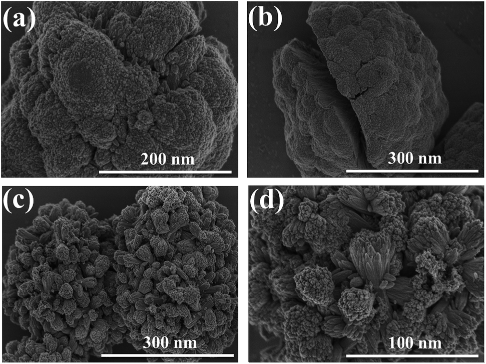 | ||
| Fig. 1 Plane-view FESEM images of cauliflower-shaped SnO2 nanospheres at (a) high resolution and (b) low resolution showing that the inside of each cauliflower is made of tiny nanorods and surface FESEM images of 3D hierarchical SnO2 nanostructures at (c) low resolution and (d) high resolution exhibiting that nanorods are grown over the entire surface of the nanosphere, respectively. | ||
Using these SnO2 nanostructures with sufficiently increased thicknesses, we have assembled both PSC and DSSC devices, respectively. The representative J–V curves (both in the forward and reverse scan) of the PSCs based on two distinct SnO2 nanostructures are displayed in Fig. 2a, and the parameters are summarized in Table 1. PSCs based on ETLs with cauliflower-shaped SnO2 nanospheres showed an average power conversion efficiency (PCEavg) of 15.05%, with a short-circuit current-density (JSC) of 20.3 mA cm−2, an open-circuit voltage (VOC) of 1030 mV, and a fill factor (FF) of 72%. With the employment of ETLs based on 3D hierarchical SnO2 nanospheres, PSCs demonstrated a significantly enhanced device performance (with a PCEavg of 17.03%) and mainly inhibited hysteresis behavior. The improved device performance of 3D hierarchical SnO2 nanospheres ETLs is due to their improved light-harvesting ability, complete pore filling, fast charge transport and reduced charge recombination. The hysteresis-free behavior is credited to the enhanced charge collection and transport at the SnO2/perovskite light-absorber interface. Optimization was checked systematically together with device reproducibility which was confirmed via statistical distribution of the device performance. Fig. 2b shows the histogram of the PCE measured for 45 individual devices with two distinct SnO2 nanostructures. These devices show a high degree of reproducibility in the PCE. As observed in Fig. 2b, the statistical analysis show that almost all devices based on 3D hierarchical SnO2 nanospheres have a higher PCE compared to the devices based on cauliflower-shaped SnO2 nanospheres. The average PCE of the devices with 3D hierarchical SnO2 nanosphere and cauliflower-shaped SnO2 nanosphere ETLs is 17.03% and 15.05%, respectively.
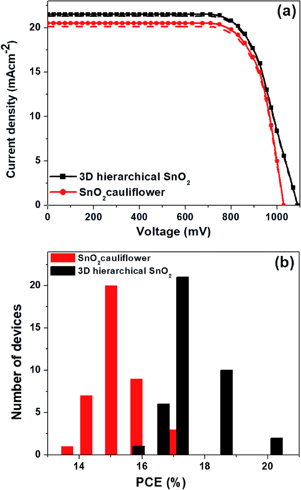 | ||
| Fig. 2 (a) Comparison of J–V curves of PSCs based on two distinct SnO2 nanostructures and (b) histograms of the corresponding PSCs showing variations in the PCE for 45 individual cells for each nanostructure. | ||
| ETL | Scan direction | J SC (mA cm−2) | V OC (mV) | FF (%) | PCEavg (%) | PCEmax (%) |
|---|---|---|---|---|---|---|
| SnO2 cauliflower | Reverse | 20.5 | 1030 | 72 | 15.20 ± 0.10 | 17.10 |
| Forward | 20.1 | 1030 | 72 | 14.90 ± 0.10 | 16.86 | |
| Average | 20.3 | 1030 | 72 | 15.05 ± 0.10 | 16.98 | |
| 3D hierarchical SnO2 | Reverse | 21.5 | 1090 | 73 | 17.10 ± 0.12 | 20.01 |
| Forward | 21.3 | 1090 | 73 | 16.94 ± 0.11 | 19.83 | |
| Average | 21.4 | 1090 | 73 | 17.03 ± 0.12 | 19.92 |
The thickness of ETLs plays a crucial part in defining the photovoltaic performance, which is optimized by properly tuning the experimental conditions in this work. The typical J–V curves of PSCs with two distinct SnO2 nanostructures with varying film thicknesses are shown in Fig. 3. The cells achieved the best performance with the thinnest ETLs (∼435 nm, in Fig. 2a). Further increase of the ETL thickness (Fig. 3) deteriorated the device performance due to poor perovskite loading into the ETLs and slow charge transport in thicker films.
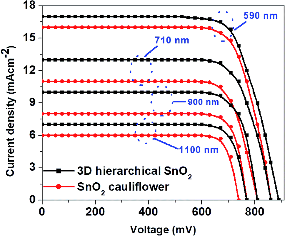 | ||
| Fig. 3 J–V curves as a function of the ETL thickness for two distinct SnO2 nanostructures. | ||
In Fig. 4a, we show the J–V curve (reverse scan) of the best performing PSC with 3D hierarchical SnO2 nanospheres. More specifically, the champion device showed the highest PCE of 20.01% with a VOC, JSC, and FF of 1155 mV, 22.8 mA cm−2, and 76%, respectively. This remarkable device efficiency of 20.01% is among the best results for PSCs with 3D hierarchical SnO2 nanospheres and is reported for the first time ever, to the best of our knowledge. In order to further confirm the reliability of the PSCs produced in this study, the steady state efficiencies of the 3D hierarchical SnO2 nanosphere based devices are also studied. As exhibited in Fig. 4b, the device showed a stable JSC of 22.8 mA cm−2 and a PCE of 20.01% at a voltage bias of 0.83 V, which is possibly initiated by the faster charge transfer and suppressed charge recombination due to the improved contact interface between the perovskite and 3D hierarchical SnO2 nanosphere based ETL. The hysteresis behavior of the best performing PSCs was also tested by collecting the J–V curves both in the forward and reverse directions as seen in Fig. 5. Negligible hysteresis is observed for these devices, thanks to the improved charge passivation and transfer at the SnO2 ETL/perovskite light-absorber interface.
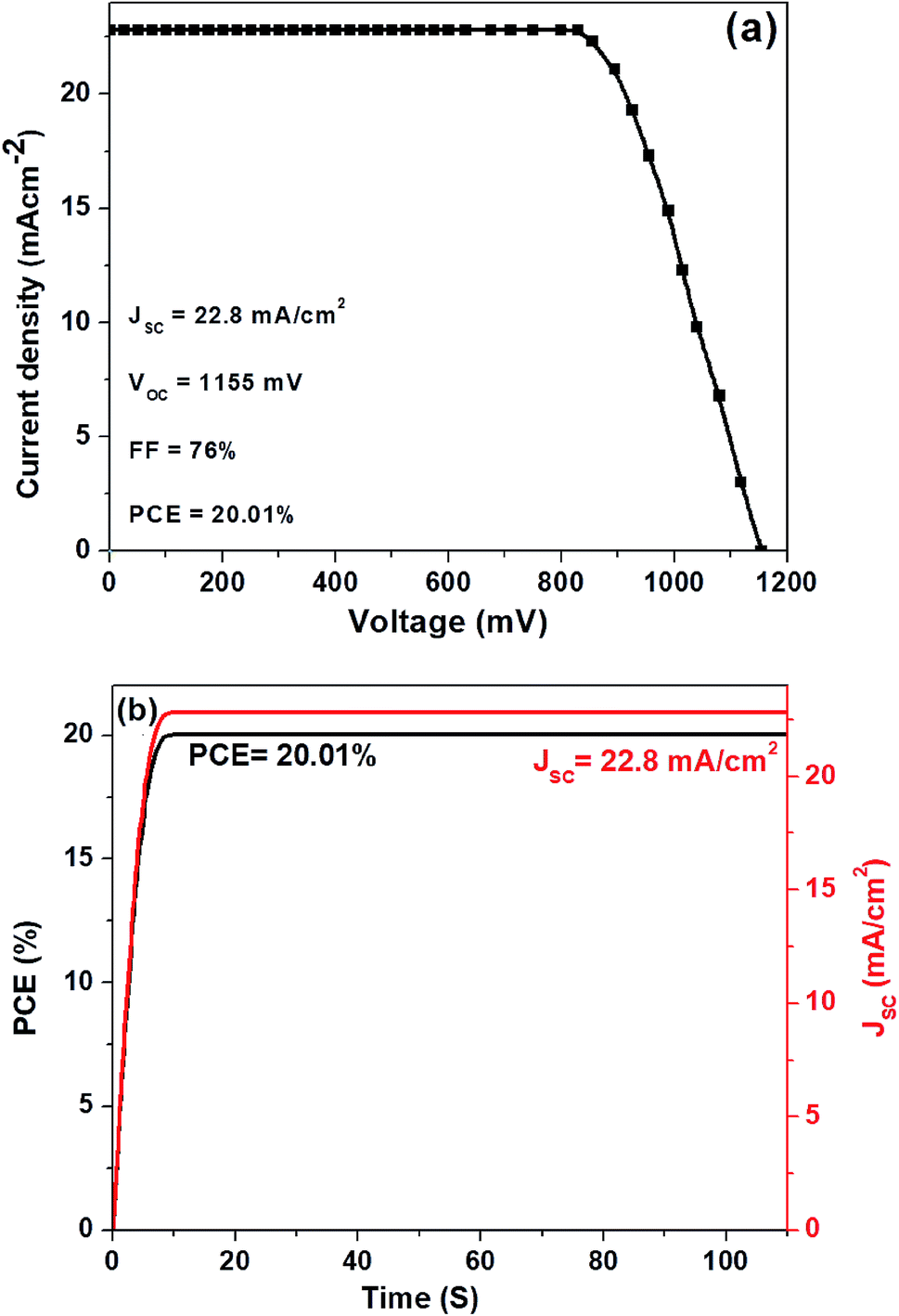 | ||
| Fig. 4 (a) J–V plot (reverse scan) for the best performing PSCs with 3D hierarchical SnO2 nanospheres and (b) the steady state efficiency of the corresponding devices measured at maximum power output. | ||
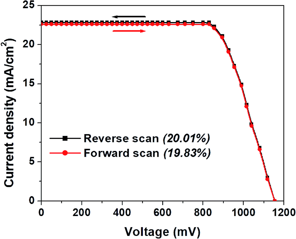 | ||
| Fig. 5 J–V plot (both in reverse and forward scans) for the best performing PSCs with 3D hierarchical SnO2 nanospheres showing their hysteresis-free behavior. | ||
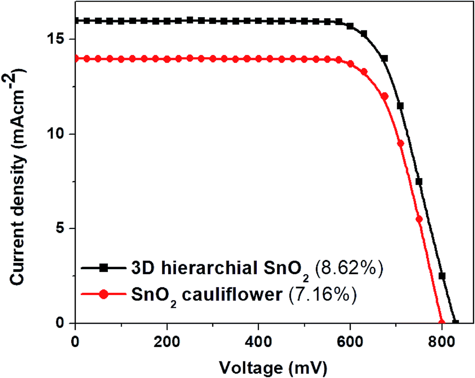
For comparison and application in DSSCs, SnO2 nanostructures with a thickness of around 8 μm were used. Fig. 6 shows the J–V plots of the DSSCs based on these two distinct photoanode films. Among these two photoanodes, the DSSCs fabricated with 3D hierarchical SnO2 nanospheres demonstrate a higher JSC due to a large amount of dye adsorption. The dye loading amount of 3D hierarchical SnO2 nanospheres was 18.56 × 10⁻⁸ mol cm−2 which was much higher than that of the cauliflower-shaped SnO2 nanospheres (8.71 × 10⁻⁸ mol cm−2). Since the JSC depends strongly on both light utilization and absorption, multiple scattering produced by the 3D hierarchical SnO2 nanospheres would enhance the paths of the incident light within the photoanode film, and thus improve the chances of dye molecules to be excited more. The VOC of 3D hierarchical SnO2 nanosphere-based DSSCs is relatively higher than that of the ones with cauliflower-shaped SnO2 nanospheres, thanks to the well interconnected structure preventing charge recombination with I3− in the electrolyte. In addition, DSSCs with 3D hierarchical SnO2 nanospheres demonstrate an improved PCE of 8.62%, which is assigned to the high dye loading and proper light confinement within the photoanode film. It is worth mentioning that the best efficiency of 10.37% (in Fig. 7) of DSSCs based on 3D hierarchical SnO2 nanospheres ranks at the top of the efficiencies of SnO2-based DSSCs reported to date.
 | ||
| Fig. 6 Comparison of J–V curves of DSSCs fabricated with two distinct SnO2 nanostructures. | ||
 | ||
| Fig. 7 Comparison of J–V curves of best performing devices of both PSCs and DSSCs based on the 3D hierarchical SnO2 nanosphere ETL. | ||
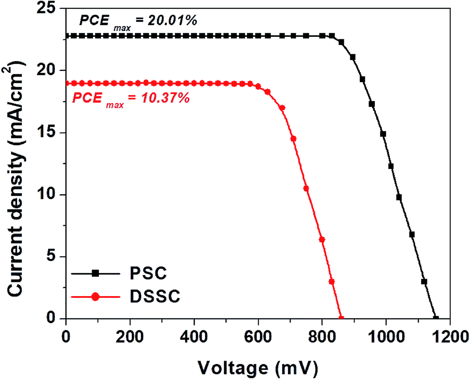
In Fig. 7, we show the J–V plots of the best performing PSCs and DSSCs based on 3D hierarchical SnO2 nanosphere films. The DSSC attained a remarkable PCEmax of 10.37% with a JSC of 18 mA cm−2, a FF of 67% and a VOC of 860 mV. The perovskite device showed a remarkably superior efficiency, demonstrating a PCEmax of 20.01%, the highest and never been reported value to date. These new findings clearly prove that, as novel nanostructures, 3D hierarchical SnO2 nanosphere films must be superior building blocks for hybrid photovoltaics to obtain better device performances than conventional SnO2 nanoparticle based films which have been extensively used in both solar energy applications and other research areas.
We also show the steady-state PL spectra (Fig. 8a) of perovskites based on different nanostructures of SnO2 to explain the reason behind the fast charge extraction capabilities of 3D hierarchical SnO2 nanostructures compared to the cauliflower-shaped SnO2 nanospheres. The perovskites formed on 3D hierarchical SnO2 nanostructures exhibit a less intense PL peak compared to cauliflower-shaped SnO2 nanospheres, which enhances electron transfer from the perovskites to the oxide layer. Moreover, an intensity-modulated photovoltage spectroscopy (IMVS) test was also performed (Fig. 8b) to evaluate the electron lifetime of perovskites deposited on different SnO2 nanostructures. A longer electron lifetime was seen for the perovskites based on 3D hierarchical SnO2 nanostructures compared to the cauliflower-shaped SnO2 nanospheres, demonstrating reduced charge recombination.
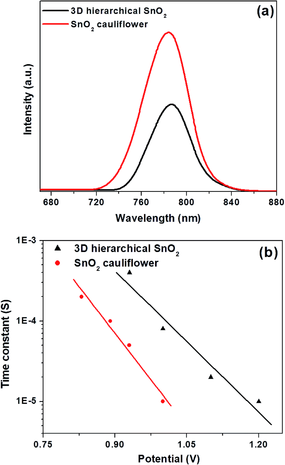 | ||
| Fig. 8 (a) Steady-state PL spectra of perovskites on different SnO2 nanostructures and (b) electron lifetime for the perovskites based on different SnO2 nanostructures. | ||
The stability of the performance of PSCs was also studied constantly in dry air. The cells based on 3D hierarchical SnO2 nanostructures showed superior long-term stability even after 100 days (Fig. S4†) compared to the cells based on cauliflower-shaped SnO2 nanospheres. The improved shelf stability of SnO2 based PSCs can be assigned to the robust nature of SnO2 against moisture and oxygen. In addition, the highly porous nature of the SnO2 nanostructures facilitates better pore filling and the formation of a better interface between the perovskite and the ETL which prevents perovskite phase separation. Thus an extended lifetime was seen for the devices constructed using SnO2 nanostructures.
4. Conclusion
To summarize, SnO2 ETLs based on novel 3D hierarchical SnO2 nanospheres have been prepared using a facile hydrothermal route for the first time ever. These ETLs not only have a large surface area, but also fast charge transport, improved light-harvesting ability and inhibited charge recombination, which are recognized through the remarkable improvement in terms of the device efficiency in both perovskite and dye sensitized solar cells. Perovskite devices were made by using a nanometer size film of 3D hierarchical SnO2 nanospheres to produce a high PCE of 20.01%. DSSCs were assembled using thicker photoanodes, demonstrating the best PCE of 10.37%, the highest ever value obtained using hierarchical SnO2 photoelectrodes. These findings obviously prove that 3D hierarchical SnO2 nanospheres have huge potential for building next generation mesoscopic photovoltaics. Additionally, these novel wide bandgap metal oxide films are anticipated to also exhibit great potential in the fields of electromagnetism, lithium batteries and sensors.Conflicts of interest
There are no conflicts to declare.Acknowledgements
The authors gratefully acknowledge the financial support from the Higher Education Commission (HEC) of Pakistan.References
- J. Lee, M. C. Orilall, S. C. Warren, M. Kamperman, F. J. DiSalvo and U. Wiesner, Nat. Mater., 2008, 7, 222 CrossRef CAS PubMed.
- H. J. Bolink, E. Coronado, J. Orozco and M. Sessolo, Adv. Mater., 2009, 21, 79–82 CrossRef CAS.
- M. F. M. Noh, C. H. Teh, R. Daik, E. L. Lim, C. C. Yap, M. A. Ibrahim, N. A. Ludin, A. R. bin Mohd Yusoff, J. Jang and M. A. M. Teridi, J. Mater. Chem. C, 2018, 6, 682–712 RSC.
- Q. Jiang, X. Zhang and J. You, Small, 2018, 14, 1801154 CrossRef PubMed.
- P. Zhang, J. Wu, T. Zhang, Y. Wang, D. Liu, H. Chen, L. Ji, C. Liu, W. Ahmad and Z. D. Chen, Adv. Mater., 2018, 30, 1703737 CrossRef PubMed.
- K. Mahmood, S. Sarwar and M. T. Mehran, RSC Adv., 2017, 7, 17044–17062 RSC.
- K. Mahmood, B. S. Swain and A. Amassian, Adv. Mater., 2015, 27, 2859–2865 CrossRef CAS PubMed.
- K. Mahmood and H. J. Sung, J. Mater. Chem. A, 2014, 2, 5408 RSC.
- K. Mahmood, A. Khalid and M. T. Mehran, Sol. Energy, 2018, 173, 496–503 CrossRef CAS.
- N. J. Jeon, J. H. Noh, Y. C. Kim, W. S. Yang, S. Ryu and S. I. Seok, Nat. Mater., 2014, 13, 897 CrossRef CAS PubMed.
- N. J. Jeon, J. H. Noh, W. S. Yang, Y. C. Kim, S. Ryu, J. Seo and S. I. Seok, Nature, 2015, 517, 476 CrossRef CAS PubMed.
- W. S. Yang, B.-W. Park, E. H. Jung, N. J. Jeon, Y. C. Kim, D. U. Lee, S. S. Shin, J. Seo, E. K. Kim and J. H. Noh, Science, 2017, 356, 1376–1379 CrossRef CAS PubMed.
- N. J. Jeon, H. Na, E. H. Jung, T.-Y. Yang, Y. G. Lee, G. Kim, H.-W. Shin, S. I. Seok, J. Lee and J. Seo, Nat. Energy, 2018, 3, 682 CrossRef CAS.
- Energy Laboratory (NREL), Best Research-Cell Efficiencies Chart, see https://www.nrel.gov/pv/assets/pdfs/pv-efficiencies-07-17-2018.pdf for National Renewable, accessed September 2018 Search PubMed.
- K. Mahmood, A. Khalid and M. T. Mehran, Sol. Energy, 2018, 173, 496–503 CrossRef CAS.
- K. Mahmood, M. T. Mehran, F. Rehman, M. S. Zafar, S. W. Ahmad and R. K. Song, ACS Omega, 2018, 3, 9648–9657 CrossRef CAS.
- K. Mahmood, A. Khalid, M. S. Zafar, F. Rehman, M. Hameed and M. T. Mehran, J. Colloid Interface Sci., 2019, 538, 426–432 CrossRef CAS PubMed.
- K. Mahmood, M. Hameed, F. Rehman, A. Khalid, M. Imran and M. T. Mehran, Appl. Phys. A, 2019, 125, 83 CrossRef.
- S. Li, P. Zhang, H. Chen, Y. Wang, D. Liu, J. Wu, H. Sarvari and Z. D. Chen, J. Power Sources, 2017, 342, 990–997 CrossRef CAS.
- T. Zhang, F. Wang, P. Zhang, Y. Wang, H. Chen, J. Li, J. Wu, L. Chen, Z. D. Chen and S. Li, Nanoscale, 2019, 11, 2871–2877 RSC.
- W. Ahmad, D. Liu, W. Ahmad, Y. Wang, P. Zhang, T. Zhang, H. Zheng, Z. D. Chen and S. Li, IEEE Journal of Photovoltaics, 2019, 9, 200–206 Search PubMed.
- T. Zhang, J. Wu, P. Zhang, W. Ahmad, Y. Wang, M. Alqahtani, H. Chen, C. Gao, Z. D. Chen, Z. Wang and S. Li, Adv. Opt. Mater., 2018, 6, 1701341 CrossRef.
- Y. Bai, Y. Fang, Y. Deng, Q. Wang, J. Zhao, X. Zheng, Y. Zhang and J. Huang, ChemSusChem, 2016, 9, 2686 CrossRef CAS PubMed.
- S. S. Mali, J. V. Patil, H. Kim and C. K. Hong, Nanoscale, 2018, 10, 8275 RSC.
- Q. Liu, M.-C. Qin, W.-J. Ke, X.-L. Zheng, Z. Chen, P.-L. Qin, L.-B. Xiong, H.-W. Lei, J.-W. Wan, J. Wen, G. Yang, J.-J. Ma, Z.-Y. Zhang and G.-J. Fang, Adv. Funct. Mater., 2016, 26, 6069 CrossRef CAS.
- S. Kumar and A. Dhar, ACS Appl. Mater. Interfaces, 2016, 8, 18309–18320 CrossRef CAS PubMed.
- Q. Jiang, Z. Chu, P. Wang, X. Yang, H. Liu, Y. Wang, Z. Yin, J. Wu, X. Zhang and J. You, Adv. Mater., 2017, 29, 1703852 CrossRef PubMed.
- H. Tao, Z. B. Ma, G. Yang, H. N. Wang, H. Long, H. Y. Zhao, P. L. Qin and G. J. Fang, Appl. Surf. Sci., 2018, 434, 1336–1343 CrossRef CAS.
- P. Zhou, J. Wu, Y. Tu, M. Zhen, J. Huo, Y. Wei and Z. Lan, Sol. Energy, 2016, 137, 579–584 CrossRef CAS.
- C. L. Wang, D. W. Zhao, C. R. Grice, W. Q. Liao, Y. Yu, A. Cimaroli, N. Shrestha, P. J. Roland, J. Chen, Z. H. Yu, P. Liu, N. Cheng, R. J. Ellingson, X. Z. Zhao and Y. F. Yan, J. Mater. Chem. A, 2016, 4, 12080–12087 RSC.
- D. Pérez-del-Rey, P. P. Boix, M. Sessolo, A. Hadipour and H. J. Bolink, J. Phys. Chem. Lett., 2018, 9, 1041–1046 CrossRef PubMed.
- K. Mahmood, A. Khalid, F. Nawaz and M. T. Mehran, J. Colloid Interface Sci., 2018, 532, 387–394 CrossRef CAS PubMed.
- Y. Lv, P. Wang, B. Cai, Q. Ma, X. Zheng, Y. Wu, Q. Jiang, J. Liu and W. -H. Zhang, Sol. RRL, 2018, 2, 1800133 CrossRef.
- Y. Chen, Z. Yang, S. Wang, X. Zheng, Y. Wu, N. Yuan, W. -H. Zhang and S. Liu, Adv. Mater., 2018, 30, 1805660 CrossRef PubMed.
- Y. Wu, P. Wang, S. Wang, Z. Wang, B. Cai, X. Zheng, Y. Chen, N. Yuan, J. Ding and W. -H. Zhang, ChemSusChem, 2018, 11, 837 CrossRef CAS PubMed.
Footnotes |
| † Electronic supplementary information (ESI) available. See DOI: 10.1039/c9na00192a |
| ‡ Both authors contributed equally to this work. |
| This journal is © The Royal Society of Chemistry 2019 |