
 Open Access Article
 This Open Access Article is licensed under a Creative Commons Attribution-Non Commercial 3.0 Unported Licence
Oriented attachment growth of monocrystalline cuprous oxide nanowires in pure water†
Jun
Meng
ae,
Chengyi
Hou
 *bc,
Hongzhi
Wang
b,
Qijin
Chi
c,
Yi
Gao
ad and
Beien
Zhu
*ad
*bc,
Hongzhi
Wang
b,
Qijin
Chi
c,
Yi
Gao
ad and
Beien
Zhu
*ad
aDivision of Interfacial Water and Key Laboratory of Interfacial Physics and Technology, Shanghai Institute of Applied Physics, Chinese Academy of Sciences, Shanghai 201800, China. E-mail: zhubeien@sinap.ac.cn
bState Key Laboratory for Modification of Chemical Fibers and Polymer Materials, College of Materials Science and Engineering, Donghua University, Shanghai, 201620, People's Republic of China. E-mail: hcy@dhu.edu.cn
cDepartment of Chemistry, Technical University of Denmark, DK-2800 Kongens Lyngby, Denmark
dShanghai Advanced Research Institute, Chinese Academy of Sciences, 201210 Shanghai, China
eUniversity of Chinese Academy of Sciences, Beijing 100049, China
First published on 25th March 2019
Abstract
As a crucial mechanism of non-classical crystallization, the oriented attachment (OA) growth of nanocrystals is of great interest in nanoscience and materials science. The OA process occurring in aqueous solution with chemical reagents has been reported many times, but there are limited studies reporting the OA growth in pure water. In this work, we report the temperature-dependent OA growth of cuprous oxide (Cu2O) nanowires in pure water through a reagent-free electrophoretic method. Our experiments demonstrate that Cu2O quantum dots randomly coalesced to form polycrystalline nanowires at room temperature, while they form monocrystalline nanowires at higher temperatures by the OA mechanism. DFT modeling and computations indicate that the water coverage on the Cu2O nanoparticles could affect the particle attachment mechanisms. This study sheds light on the understanding of the effects of water molecules on the OA mechanism and shows new approaches for better controllable non-classical crystallization in pure water.
Introduction
In the last few decades, non-classical crystallization has caught great attention since it can offer new chemical routes to the controllable synthesis of nanomaterials.1–3 A crucial mechanism of non-classical crystallization is that a crystal grows through the oriented attachment (OA) of nanoscale “building blocks” rather than individual atoms, ions or molecules growing to nucleated seeds.4–11 The OA mechanism differs significantly from random coalescence (RC) in the orientation of the crystal lattice at the grain boundary. In the RC process, there is no particular preference for the attachment and the lattice planes are randomly orientated between domains.12 In contrast, with the OA mechanism the nanoparticles attach in a common crystallographic orientation and there is a perfect alignment of the planes.13 Highly ordered iso-oriented or monocrystalline materials can be formed through OA, which makes this mechanism significantly important in nanoscience and materials science. Various types of external factors that could affect the OA mechanisms have been studied,3,14–20 including adding additives,21 changing concentration22 and electric field treatment.23 Many studies have shown that ligands have a strong influence on the crystal growth process, like some organic molecules24–26 and DNA.27,28 In these studies, the OA process is mostly reported occurring in chemical solutions, but the OA process in pure water has not been well studied.Recent studies have proven that adsorbed water molecules not only affect the surface properties of nanostructured materials,29–32 but also alter their behaviors such as mobility, shape, and chemical activity in reactions.33–36 In particular, Loh et al. have just discovered water-mediated metastable gold complexes during a three-step nucleation process of gold nanocrystals when a supersaturated aqueous solution was used.36 Thomele et al. have recently reported that water vapor could induce the self-organization of MgO nanocubes into one-dimensional crystalline structures.37 These results suggest that the water molecules may have a direct impact on nanomaterial crystallization. Thus, studying the OA growth in a pure water environment is of particular interest.
In this work, we firstly synthesized a highly active semiconductor nanocatalyst cuprous oxide (Cu2O) in pure water through a reagent-free electrophoretic method, which can minimize (or exclude) all possible side effects from chemical reagents. In the experiments, Cu2O monocrystalline nanowires (MNs) were formed at high temperatures through an OA process (near the water boiling point 90–95 °C), while polycrystalline nanowires (PNs) were generated at low temperatures (near the ice point to room temperature). Theoretical analyses show that the water coverage on the (110) surface of Cu2O quantum dots (QDs) decreases sharply by increasing the temperature. It is proposed that the lowered water coverage on Cu2O(110) surfaces exposes the (110) facet and makes it a preferable facet for the OA growth of nanowires. This revealed effect provides a novel way to utilize water adsorption for tunable non-classical crystallization.
Experimental
With the aim of studying the OA process in a pure water environment, the chemical environment should be as simple as possible to avoid any undesirable effects from chemical reagents (e.g., salt precursors, the electrolytic solution, surfactants, buffers, etc.). A reagent-free electrolysis apparatus under the laboratory atmospheric environment was thus used in our experiments (Fig. 1). Briefly, bulk metals were immersed in Milli-Q water (18.2 MΩ cm, total organic carbon values < 5 ppb, pH = 6.9, and redox potential is 10 mV) with a direct-current electric field applied to the metal electrodes. The target metal (copper in this case) was used as an anode, while Pt was used as a cathode. The gap between the two metal electrodes varied from micrometers to centimeters, resulting in a DC field with an intensity of several volts per centimeter (typically 3–30 V cm−1, but not limited to this range). The height of the liquid cell is around 1 centimeter. This strategy is based on our previous innovations.38,39 Metal oxide quantum dots (QDs) are generated from the anode upon electrolytic oxidation. The generated QDs undergo electrophoretic assembly during swimming between the two electrodes. Cu2O QDs were found to be produced in water around the anode under ambient conditions.38 Such nanocrystals are endowed with built-in dipoles under the electric field, and thus are able to assemble into wire-like nanostructures via dipole–dipole interactions.40–42 By altering the water solution temperature (between the ice point and boiling point in order to maintain a liquid cell), the water coverage on QDs can be finely tuned, offering the opportunity for investigating the influence of water adsorption on the non-classical crystallization of metal oxide nanostructures.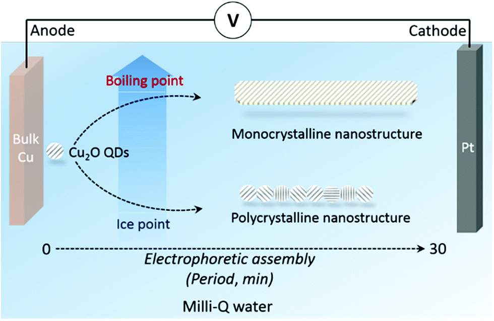 | ||
| Fig. 1 Schematic of the apparatus used in the reagent-free electrophoretic synthesis of cuprous oxide nanostructures at different environmental temperatures. A 30 min electrolysis period with an applied electric field intensity of 26 V cm−1 was typically employed for the synthesis and electrophoretic assembly of cuprous nanowires. | ||
The nanostructure formation is captured with the assistance of transmission electron microscopy (TEM) images. The images were taken using a FEI Tecnai T20 G2 (200 kV accelerating voltage; information limit ∼ 0.24 nm) and FEI Titan E-Cell 80-300 ST TEM (300 kV accelerating voltage; information limit < 0.08 nm). It is worth mentioning that in this dynamic electrophoretic system, the nanomaterials simultaneously assemble and swim between the two electrodes, and therefore the location of certain sample groups varies along with the morphology development.38,39 Although a real-time and in situ monitoring tool is unavailable, we successfully captured the nanostructure evolution through ex situ TEM imaging. In detail, the suspension containing QDs was collected from the area around the anode after 5 min synthesis. The suspension containing nanowires was collected from the area around the cathode after 30 min.
In control experiments, other variables such as the reaction time (related to morphology development), additional light irradiation (may change the surface properties of semiconductors), and exposure to oxygen (may cause oxidation of cuprous oxide) are regulated carefully. By ruling out the above factors, we focus on one major factor that induces the monocrystalline growth of cuprous oxide nanowires in this work.
Results and discussion
As shown in Fig. 2a–c, polycrystalline Cu2O nanowires that have a length of around 60–100 nm and a width of approximately 5 nm were produced at 25 °C. A high-resolution TEM (HRTEM) image regarding the detailed structure of a polycrystalline nanowire (PN) is shown in Fig. 3a and S1.† The observations of the QDs before the nanowire formation (Fig. 2a) and the lattice fringes shown in Fig. 3a give evidence that the PNs are formed by the attachment of Cu2O QDs. X-ray photoelectron spectroscopy (XPS) and electron energy loss spectroscopy (EELS) spectra of the nanomaterials (Fig. S2 and S3†) confirm the formation of pure Cu2O. The polycrystalline nature of the assembled Cu2O nanowires is confirmed by the fast Fourier transform (FFT) pattern (the inset in Fig. 2c). Moreover, the HRTEM image (Fig. 3a) demonstrates that the PNs have a lattice spacing of 0.25 and 0.22 nm, corresponding to the (111) and (200) planes of cubic Cu2O, respectively. Apparently, the attachment of Cu2O QDs in water proceeded by the RC mechanism at room temperature. | ||
| Fig. 2 Microscopic characterization of Cu2O nanostructures. (a) HRTEM image of individual Cu2O QDs formed at 25 °C. (b) TEM image of Cu2O polycrystalline nanowires assembled from QDs at 25 °C. (c) HRTEM image of a single polycrystalline nanowire of Cu2O at 25 °C. The inset shows an FFT pattern corresponding to (c). Two major planes (110) and (111) are indicated. (d) TEM image of Cu2O QDs synthesized at 90 °C. (e) TEM image of Cu2O monocrystalline nanowires grown at 90 °C. (f) HRTEM image of a monocrystalline nanowire of Cu2O at 90 °C. The inset shows the FFT pattern of (f). One major plane (110) of cubic Cu2O is indicated. | ||
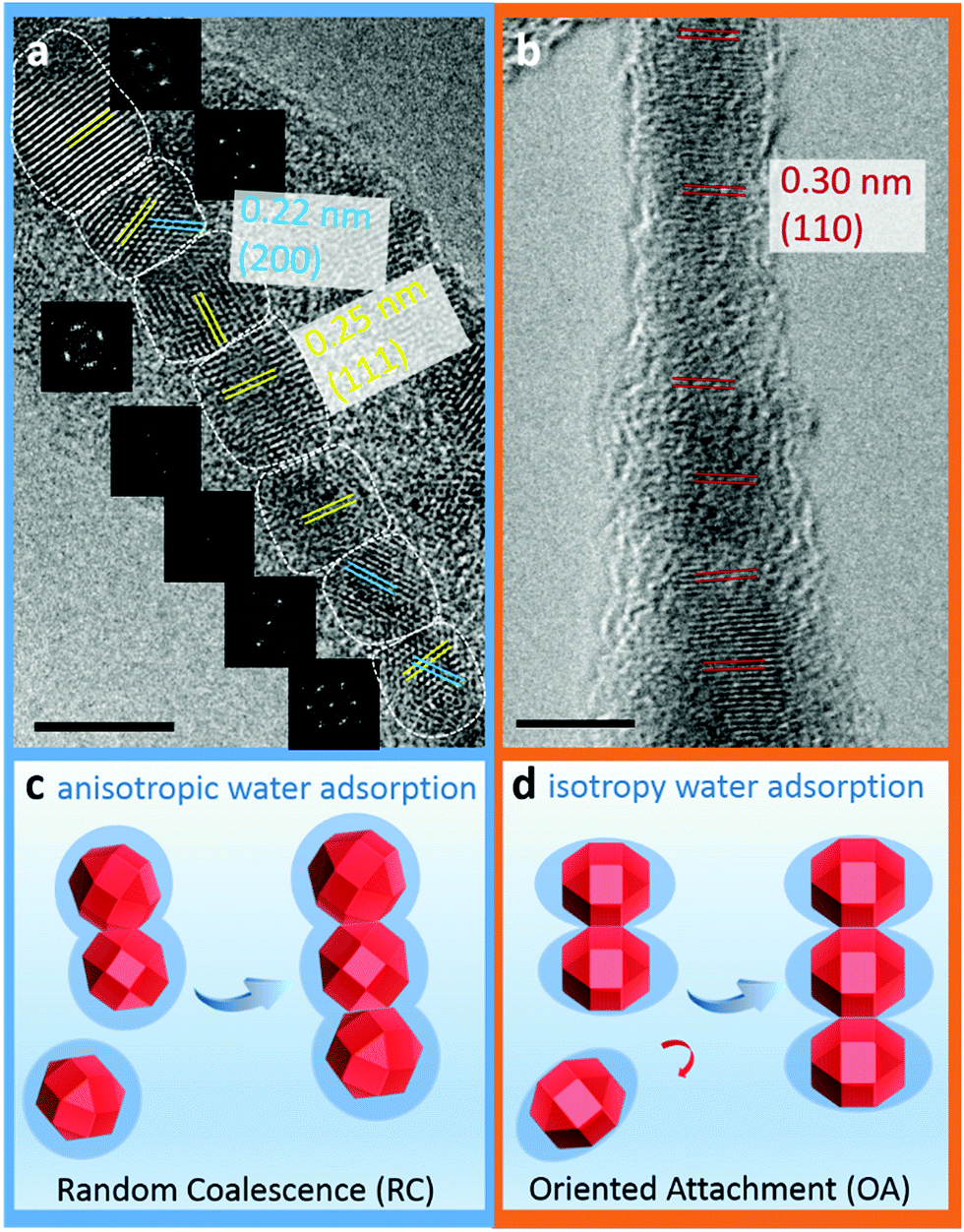 | ||
| Fig. 3 Detailed structural information of nanowires assembled at 25 °C and 90 °C with the proposed formation mechanisms of crystal growth. (a) Detailed information of a typical polycrystalline Cu2O nanowire assembled at 25 °C. Individual crystals and their FFT patterns are presented. (111) and (200) planes of Cu2O are indicated by yellow and blue lines, respectively. (b) Detailed information of a typical monocrystalline Cu2O nanowire synthesized at 90 °C. (110) planes of Cu2O are indicated by red lines. A long-range order along the [110] direction in the crystal orientation is visible. (c) Illustration of a random attachment growth pattern of Cu2O QDs at room temperature. (d) Illustration of an oriented attachment growth pattern of Cu2O QDs along the [110] direction at the higher temperature. Scale bars are 5 nm. | ||
At relatively high temperatures (e.g. 90 °C), interestingly, the single crystallization of Cu2O nanowires was found to be predominant. As shown in Fig. 2d, the nanoparticle building blocks are no longer monodisperse but coalesced into nanoparticles mostly composed of two single QDs. Several examples of the initial transient of coalescence of two Cu2O nanocrystals are shown in Fig. S4.† After electrophoretic assembly, the Cu2O QDs converted to 1D Cu2O nanowires (see XPS results in Fig. S2†). Most importantly, these nanowires are well-crystallized monocrystalline nanowires (MNs) and can suspend on a holey carbon support film for recording HRTEM images and corresponding FFT patterns (Fig. 2f, 3b, and S5†). Preassembled particles, preassembled wires, and well-assembled wires can be observed in a TEM specimen (Fig. S6†). The coexistence of preassembled nanocrystals and nanowires strongly indicates that the long-range ordered MNs are formed via particle attachment, particularly following the OA mechanism. Clearly, the Cu2O MNs have a unique ultrathin wire-like morphology. As a comparison, the classic crystallization tends to form cubic-like or sphere-like micro-sized structures.43,44 The interfringe distance of the monocrystalline nanowire is measured to be 0.30 nm, corresponding to the (110) plane of cubic Cu2O (Fig. 3b). These planes are slightly misaligned (misoriented by ∼3° as shown in Fig. 3b), as the OA mechanism is the direct coalescence of QDs, and they may keep their initial configurations. Such incorporation of defects (twins, stacking faults, and misorientation) is the important feature of the OA mechanism.4,45–47 All these experimental observations clearly show that the attachment pattern of Cu2O QDs switches from RC to OA by simply tuning the solution temperature, i.e. from a cold water solution to a hot water solution. It should be noticed that the TEM ion-beam induced amorphization of the MN can be seen in Fig. 2f and 3b. It is very common that TEM specimens are covered by a (partly) amorphous surface layer due to the exposure to carbon containing molecules during specimen transfer or operating in an imperfect TEM environment. This surface coating has nothing to do with the growth of the MN.
Note that the orientation of Cu2O nanocrystals is not under the control of the electric field during the synthesis. Although it is believed that the electric-field-induced dipole–dipole interaction could play an important role in one-dimensional attachment of particles in the electrophoretic assembly,40–42 our results show that the dipole–dipole interaction has very limited effect on particle orientation and crystallization under the present experimental conditions. In this work, the local electric fields are a prerequisite for the construction of a one-dimensional structure of nanowires but not responsible for the different nanowire growth mechanisms at different temperatures.
To understand the OA growth of Cu2O MNs at the higher temperature, we firstly check the TEM images and corresponding SAED patterns of QDs synthesized after ∼5 min at 25 °C, coalesced QDs synthesized after ∼1 min at 90 °C and further coalesced QDs synthesized after ∼5 min at 90 °C. There is no significant crystallographic structure difference between the QDs synthesized at low temperatures and high temperatures (Fig. S7†). A previous study has reported that, in aqueous solution, hydrated Au atoms have to be partially dehydrated to form nanoclusters.36 The water molecules near the small clusters could form a barrier obstructing the further coalescence process. In this work, how the water molecules may affect the particle attachment process is evaluated by theoretical calculations. We applied DFT calculations to investigate the interaction between water molecules and different surfaces of the Cu2O QDs. There are three types of low-index crystalline facet surfaces on Cu2O nanocrystals, i.e., (111), (100) and (110), among which the Cu2O(110) surface has the lowest surface energy (0.026 eV Å−2)48 and the weakest bonding ability to water molecules (Table 1). The dissociative adsorption of water also has been carefully studied. For the Cu2O(100)![[thin space (1/6-em)]](https://www.rsc.org/images/entities/char_2009.gif) :O surface, the dissociative adsorption energy is −0.56 eV, which is less stable than the associative adsorption energy −0.62 eV. For the Cu2O(110):CuO and Cu2O(111):O surfaces, the H atom attached to the surface O atom tends to bond to the surface OH group and leads to water molecular adsorption. The dissociative adsorption is unfavorable on these surfaces. Based on the previous prediction of the effect of water molecules, we quantify the water coverages on Cu2O (111), (100) and (110) facets under our experimental conditions by combining the Langmuir adsorption isotherm and DFT calculations (see the Computational method).
:O surface, the dissociative adsorption energy is −0.56 eV, which is less stable than the associative adsorption energy −0.62 eV. For the Cu2O(110):CuO and Cu2O(111):O surfaces, the H atom attached to the surface O atom tends to bond to the surface OH group and leads to water molecular adsorption. The dissociative adsorption is unfavorable on these surfaces. Based on the previous prediction of the effect of water molecules, we quantify the water coverages on Cu2O (111), (100) and (110) facets under our experimental conditions by combining the Langmuir adsorption isotherm and DFT calculations (see the Computational method).
| E ads (eV) | |
|---|---|
| (3 × 3) Cu2O(100):O |
−0.62 |
| (1 × 1) Cu2O(100):O |
−0.57 |
| (3 × 2) Cu2O(110):CuO |
−0.36 |
| (1 × 1) Cu2O(110):CuO |
−0.35 |
| (2 × 2) Cu2O(111):O |
−0.81 |
| (1 × 1) Cu2O(111):O |
−0.83 |
Based on the calculated parameters, the coverages of water on the Cu2O surface under the present experimental conditions are plotted against temperatures, and the relationship is shown in Fig. 4. The pressure is 98 Pa according to the height of water under the experimental conditions calculated using P = ρgh (h = 1 cm). In the calculations, the temperature changes from 0 to 100 °C. The modelling results provide a reasonable explanation of the experimental results. At 25 °C, the water coverage values on (100), (110), (111) surfaces are all approximately 1. Individual Cu2O QDs coalesce randomly since all the facets are equally protected by the adsorbed water molecules. Fig. 3c displays a sketch describing this process. Cu2O QDs may adhere to each other from any crystallographic orientation to form PNs. With the increase of temperature, the water coverage decreases only on the (110) surface. At 90 °C, the water coverage on the (110) surface decreases sharply to 0.21. The change of water coverage on the Cu2O(110):CuO surface from 25 °C to 90 °C is simulated, and typical images are shown in Fig. 5 according to the results predicted by the theoretical modelling. Without the protection of the adsorbed water molecules, the (110) facets are largely exposed and could promote the directional attachment of QDs, triggering an OA crystallization process as shown in Fig. 3d. As an example, an HRTEM image in the inset of Fig. 4 shows the observed oriented attachment of two Cu2O QDs along the [110] direction at 90 °C. This facet-selective particle junction results in the well-crystallized Cu2O MNs observed in the experiment.
 | ||
| Fig. 4 When P = 98 Pa, the water coverages of Cu2O(100):O, Cu2O(110):CuO, and Cu2O(111):O surfaces vary with the temperature. The inset is a TEM picture of the observed attachment of two Cu2O QDs along the [110] direction at 90 °C. | ||
 | ||
| Fig. 5 Simulated images to follow the changes of the water coverage on the Cu2O(110):CuO surface at 25 °C, 45 °C, 70 °C and 90 °C. | ||
Computational method
The Langmuir adsorption isotherm49 describes the equilibrium surface coverage of the target molecule at a given temperature and under certain pressure by, | (1) |
 | (2) |
The adsorption energy Eads of H2O molecules on Cu2O surfaces is obtained by DFT calculations using eqn (3)
| Eads = EH2O/slab − Eslab − EH2O | (3) |
:O, Cu2O(110):CuO, and Cu2O(111):O are modeled to obtain the adsorption energies, which have relatively lower surface energies according to Soon et al.48 A (3 × 3) slab for the (100) surface, (3 × 2) slab for the (110) surface and (2 × 2) slab for the (111) surface are modeled. Each of these slabs contains 5 periodic layers. The 2 bottom periodic layers are fixed and the others are fully relaxed. A vacuum layer of 15 Å is employed to prevent interactions between the repeated slabs. All of the calculations are performed using the Vienna ab initio simulation package (VASP)50 with the projector-augmented wave (PAW) potentials51,52 and the Perdew–Burke–Ernzerhof (PBE) exchange-correlation functional based on the GGA approximation.53 The cutoff energy is selected to be 450 eV and the unit cell lattice parameter is 4.31 Å. All the calculations are fully spin polarized. The convergence of the electronic self-consistent energy is 10−5 eV, and the force convergence criterion in a conjugate-gradient algorithm is 0.01 eV Å−1. The optimized structures are given in Fig. S9.† The calculated results are compared in Table 1.
Note that the Langmuir isotherm assumes that there is no lateral interaction between the adsorbates. To verify the appropriateness of using the Langmuir isotherm, in this case, the (1 × 1) slab for each surface is also modeled to obtain the adsorption energy of monolayer water. It is found that there is little difference between the adsorption energy of monomer water adsorption and monolayer water adsorption on the surfaces, indicating negligible lateral interactions (Table 1). Optimized structures are given in Fig. S10.† The Sads is considered to be zero with the assumption that the adsorbed molecule is isolated and sticks on the adsorption site steadily. The Sliquid can be acquired according to the data from NIST-JANAF Thermochemical Tables54 (Fig. S11†).
Conclusions
In conclusion, we report that the OA growth of monocrystalline Cu2O nanowires occurs in pure water at elevate temperatures. The experimental findings show a striking crystalline change of the as-synthesized nanowires from the polycrystalline phase to the monocrystalline phase when the water temperature is elevated from 25 to 90 °C in a reagent-free electrophoretic synthesis. The detailed microscopic analysis and theoretical modeling indicate that the reduced water coverage on the (110) facet of Cu2O QDs at 90 °C facilitates the oriented attachment along the [110] direction. It is suggested that the local water environment could play a key role in determining the attachment pattern of nanoparticles in aqueous solution. In general, this study could offer some crucial clues in uncovering the detailed effects of water on non-classical crystallization such as OA and open a new perspective for ongoing investigations along the related research lines.Conflicts of interest
There are no conflicts to declare.Acknowledgements
B. Z. thanks the National Natural Science Foundation of China (11604357), the Natural Science Foundation of Shanghai (16ZR1443200), and the Youth Innovation Promotion Association of Chinese Academy of Sciences. Y. G. acknowledges the financial support from the National Natural Science Foundation of China (11574340, 21773287). C. H. acknowledges the Natural Science Foundation of China (51603037) and the Shanghai Natural Science Foundation (16ZR1401500). Q. C. is grateful to the DFF-the Danish Council for Technology and Production Sciences (Project No. 12-127447). The authors thank the Special Program for Applied Research on Super Computation of the NSFC-Guangdong Joint Fund (the second phase). The computational resources utilized in this work were provided by the Shanghai Supercomputer Center, National Supercomputer Centers in Tianjin, Shenzhen.Notes and references
- J. Baumgartner, A. Dey, P. H. H. Bomans, C. Le Coadou, P. Fratzl, N. A. J. M. Sommerdijk and D. Faivre, Nat. Mater., 2013, 12, 310–314 CrossRef CAS PubMed.
- J. F. Banfield, S. A. Welch, H. Zhang, T. T. Ebert and R. L. Penn, Science, 2000, 289, 751–754 CrossRef CAS.
- J. J. De Yoreo, P. Gilbert, N. Sommerdijk, R. L. Penn, S. Whitelam, D. Joester, H. Z. Zhang, J. D. Rimer, A. Navrotsky, J. F. Banfield, A. F. Wallace, F. M. Michel, F. C. Meldrum, H. Colfen and P. M. Dove, Science, 2015, 349, aaa6760 CrossRef PubMed.
- R. L. Penn and J. F. Banfield, Science, 1998, 281, 969–971 CrossRef CAS PubMed.
- D. Li, M. H. Nielsen, J. R. I. Lee, C. Frandsen, J. F. Banfield and J. J. De Yoreo, Science, 2012, 336, 1014–1018 CrossRef CAS PubMed.
- M. Gong, A. Kirkeminde and S. Ren, Sci. Rep., 2013, 3, 2092 CrossRef PubMed.
- M. P. Boneschanscher, W. H. Evers, J. J. Geuchies, T. Altantzis, B. Goris, F. T. Rabouw, S. A. P. van Rossum, H. S. J. van der Zant, L. D. A. Siebbeles, G. Van Tendeloo, I. Swart, J. Hilhorst, A. V. Petukhov, S. Bals and D. Vanmaekelbergh, Science, 2014, 344, 1377–1380 CrossRef CAS PubMed.
- C. Viedma, J. M. McBride, B. Kahr and P. Cintas, Angew. Chem., Int. Ed., 2013, 52, 10545–10548 CrossRef CAS PubMed.
- B. Y. Xia, H. B. Wu, Y. Yan, X. W. Lou and X. Wang, J. Am. Chem. Soc., 2013, 135, 9480–9485 CrossRef CAS PubMed.
- C. Schliehe, B. H. Juarez, M. Pelletier, S. Jander, D. Greshnykh, M. Nagel, A. Meyer, S. Foerster, A. Kornowski, C. Klinke and H. Weller, Science, 2010, 329, 550–553 CrossRef CAS PubMed.
- Z. P. Zhang, H. P. Sun, X. Q. Shao, D. F. Li, H. D. Yu and M. Y. Han, Adv. Mater., 2005, 17, 42–47 CrossRef CAS.
- H. Zheng, R. K. Smith, Y.-w. Jun, C. Kisielowski, U. Dahmen and A. P. Alivisatos, Science, 2009, 324, 1309–1312 CrossRef CAS PubMed.
- M. Niederberger and H. Colfen, Phys. Chem. Chem. Phys., 2006, 8, 3271–3287 RSC.
- M. L. Sushko and K. M. Rosso, Nanoscale, 2016, 8, 19714–19725 RSC.
- Z. Zhuang, J. Zhang, F. Huang, Y. Wang and Z. Lin, Phys. Chem. Chem. Phys., 2009, 11, 8516–8521 RSC.
- K. K. Sand, J. D. Rodriguez-Blanco, E. Makovicky, L. G. Benning and S. L. S. Stipp, Cryst. Growth Des., 2012, 12, 842–853 CrossRef CAS.
- R. P. Sear, Int. Mater. Rev., 2012, 57, 328–356 CrossRef CAS.
- M. Raju, A. C. T. van Duin and K. A. Fichthorn, Nano Lett., 2014, 14, 1836–1842 CrossRef CAS PubMed.
- C. G. Lu and Z. Y. Tang, Adv. Mater., 2016, 28, 1096–1108 CrossRef CAS PubMed.
- C. Pacholski, A. Kornowski and H. Weller, Angew. Chem., Int. Ed., 2002, 41, 1188–1191 CrossRef CAS PubMed.
- M. Adachi, Y. Murata, J. Takao, J. T. Jiu, M. Sakamoto and F. M. Wang, J. Am. Chem. Soc., 2004, 126, 14943–14949 CrossRef CAS PubMed.
- S. M. Yin, Y. F. Yuan, S. Y. Guo, Z. H. Ren and G. R. Han, CrystEngComm, 2016, 18, 7849–7854 RSC.
- J. Fang, P. M. Leufke, R. Kruk, D. Wang, T. Scherer and H. Hahn, Nano Today, 2010, 5, 175–182 CrossRef CAS.
- Y. Yin and A. P. Alivisatos, Nature, 2005, 437, 664–670 CrossRef CAS PubMed.
- C. Zhu, S. Liang, E. Song, Y. Zhou, W. Wang, F. Shan, Y. Shi, C. Hao, K. Yin, T. Zhang, J. Liu, H. Zheng and L. Sun, Nat. Commun., 2018, 9, 421 CrossRef PubMed.
- J. M. Yuk, J. Park, P. Ercius, K. Kim, D. J. Hellebusch, M. F. Crommie, J. Y. Lee, A. Zettl and A. P. Alivisatos, Science, 2012, 336, 61–64 CrossRef CAS PubMed.
- L. Zhou, W. Li, Z. Chen, E. Ju, J. Ren and X. Qu, Chem.–Eur. J., 2015, 21, 2930–2935 CrossRef CAS PubMed.
- Z. Chen, C. Liu, F. Cao, J. Ren and X. Qu, Chem. Soc. Rev., 2018, 47, 4017–4072 RSC.
- J. R. Yang, H. P. Fang and Y. Gao, J. Phys. Chem. Lett., 2016, 7, 1788–1793 CrossRef CAS PubMed.
- Y. D. Li and Y. Gao, Phys. Rev. Lett., 2014, 112 CAS.
- M. Farnesi Camellone, F. Negreiros Ribeiro, L. Szabová, Y. Tateyama and S. Fabris, J. Am. Chem. Soc., 2016, 138, 11560–11567 CrossRef CAS PubMed.
- J. Saavedra, H. A. Doan, C. J. Pursell, L. C. Grabow and B. D. Chandler, Science, 2014, 345, 1599–1602 CrossRef CAS PubMed.
- J. Mu, C. Hou, H. Wang, Y. Li, Q. Zhang and M. Zhu, Sci. Adv., 2015, 1, e1500533 CrossRef.
- B. Zhu, Z. Xu, C. Wang and Y. Gao, Nano Lett., 2016, 16, 2628–2632 CrossRef CAS PubMed.
- P. L. Hansen, J. B. Wagner, S. Helveg, J. R. Rostrup-Nielsen, B. S. Clausen and H. Topsøe, Science, 2002, 295, 2053–2055 CrossRef CAS PubMed.
- N. D. Loh, S. Sen, M. Bosman, S. F. Tan, J. Zhong, C. A. Nijhuis, P. Král, P. Matsudaira and U. Mirsaidov, Nat. Chem., 2016, 9, 77 Search PubMed.
- D. Thomele, G. R. Bourret, J. Bernardi, M. Bockstedte and O. Diwald, Angew. Chem., Int. Ed., 2017, 56, 1407–1410 CrossRef CAS PubMed.
- C. Y. Hou, M. W. Zhang, T. Kasama, C. Engelbrekt, L. L. Zhang, H. Z. Wang and Q. J. Chi, Adv. Mater., 2016, 28, 4097–4104 CrossRef CAS PubMed.
- C. Hou, M. Zhang, L. Zhang, Y. Tang, H. Wang and Q. Chi, Chem. Mater., 2017, 29, 1439–1446 CrossRef CAS.
- K. D. Hermanson, S. O. Lumsdon, J. P. Williams, E. W. Kaler and O. D. Velev, Science, 2001, 294, 1082–1086 CrossRef CAS PubMed.
- L. Dong, J. Bush, V. Chirayos, R. Solanki, J. Jiao, Y. Ono, J. J. Conley and B. D. Ulrich, Nano Lett., 2005, 5, 2112–2115 CrossRef CAS.
- A. S. Negi, K. Sengupta and A. K. Sood, Langmuir, 2005, 21, 11623–11627 CrossRef CAS PubMed.
- H. Zhang, Q. Zhu, Y. Zhang, Y. Wang, L. Zhao and B. Yu, Adv. Funct. Mater., 2007, 17, 2766–2771 CrossRef CAS.
- X. Lan, J. Zhang, H. Gao and T. Wang, CrystEngComm, 2010, 13, 633–636 RSC.
- W. Lv, W. He, X. Wang, Y. Niu, H. Cao, J. H. Dickerson and Z. Wang, Nanoscale, 2014, 6, 2531–2547 RSC.
- H. Zhang and J. F. Banfield, CrystEngComm, 2014, 16, 1568–1578 RSC.
- J. Zhang, F. Huang and Z. Lin, Nanoscale, 2010, 2, 18–34 RSC.
- A. Soon, M. Todorova, B. Delley and C. Stampfl, Phys. Rev. B, 2007, 75, 125420 CrossRef.
- I. Langmuir, J. Am. Chem. Soc., 1918, 40, 1361–1403 CrossRef CAS.
- G. Kresse and J. Hafner, Phys. Rev. B, 1993, 47, 558–561 CrossRef CAS.
- G. Kresse and D. Joubert, Phys. Rev. B, 1999, 59, 1758–1775 CrossRef CAS.
- P. E. Blochl, O. Jepsen and O. K. Andersen, Phys. Rev. B, 1994, 49, 16223–16233 CrossRef CAS.
- J. P. Perdew, J. A. Chevary, S. H. Vosko, K. A. Jackson, M. R. Pederson, D. J. Singh and C. Fiolhais, Phys. Rev. B, 1992, 46, 6671–6687 CrossRef CAS.
- J. M. W. Chase, C. A. Davies, J. R. Downey Jr, D. J. Frurip, R. A. McDonald, and A. N. Syverud, NIST-JANAF Thermochemical Tables, http://kinetics.nist.gov/janaf/, accessed 09, 2016 Search PubMed.
Footnote |
| † Electronic supplementary information (ESI) available. See DOI: 10.1039/c8na00374b |
| This journal is © The Royal Society of Chemistry 2019 |