
 Open Access Article
 This Open Access Article is licensed under a Creative Commons Attribution-Non Commercial 3.0 Unported Licence
Vortex fluidic mediated transformation of graphite into highly conducting graphene scrolls†
Kasturi
Vimalanathan
a,
Irene
Suarez-Martinez
 b,
M. Chandramalika R.
Peiris
c,
Joshua
Antonio
c,
Carla
de Tomas
b,
Yichao
Zou
d,
Jin
Zou
d,
Xiaofei
Duan
e,
Robert N.
Lamb
e,
David P.
Harvey
a,
Thaar M. D.
Alharbi
a,
Christopher T.
Gibson
af,
Nigel A.
Marks
b,
Nadim
Darwish
*c and
Colin L.
Raston
*a
b,
M. Chandramalika R.
Peiris
c,
Joshua
Antonio
c,
Carla
de Tomas
b,
Yichao
Zou
d,
Jin
Zou
d,
Xiaofei
Duan
e,
Robert N.
Lamb
e,
David P.
Harvey
a,
Thaar M. D.
Alharbi
a,
Christopher T.
Gibson
af,
Nigel A.
Marks
b,
Nadim
Darwish
*c and
Colin L.
Raston
*a
aFlinders Institute for Nanoscale Science & Technology, College of Science and Engineering, Flinders University, Adelaide, SA 5001, Australia. E-mail: colin.raston@flinders.edu.au
bDepartment of Physics and Astronomy, Curtin University, Bentley Campus, Perth, WA 6102, Australia
cSchool of Molecular and Life Sciences, Curtin Institute of Functional Molecule and Interfaces, Curtin University, Bentley, WA 6102, Australia. E-mail: nadim.darwish@curtin.edu.au
dSchool of Engineering, The University of Queensland, Brisbane, QLD 4072, Australia
eTrace Analysis for Chemical, Earth and Environmental Sciences (TrACEES), The University of Melbourne, Victoria 3010, Australia
fFlinders Microscopy and Microanalysis, College of Science and Engineering, Flinders University, Adelaide, South Australia 5042, Australia
First published on 7th June 2019
Abstract
Two-dimensional graphene has remarkable properties that are revolutionary in many applications. Scrolling monolayer graphene with precise tunability would create further potential for niche applications but this has proved challenging. We have now established the ability to fabricate monolayer graphene scrolls in high yield directly from graphite flakes under non-equilibrium conditions at room temperature in dynamic thin films of liquid. Using conductive atomic force microscopy we demonstrate that the graphene scrolls form highly conducting electrical contacts to highly oriented pyrolytic graphite (HOPG). These highly conducting graphite–graphene contacts are attractive for the fabrication of interconnects in microcircuits and align with the increasing interest in building all sp2-carbon circuits. Above a temperature of 450 °C the scrolls unravel into buckled graphene sheets, and this process is understood on a theoretical basis. These findings augur well for new applications, in particular for incorporating the scrolls into miniaturized electronic devices.
Introduction
Two-dimensional (2D) graphene has captured the attention of the research community due to its exquisite electrical, thermal and mechanical properties1–3 and promising capabilities in many and diverse applications, in particular for the next generation of transparent conductive electrodes.4–10 However, the main challenge is that free-standing monolayer graphene films are hard to produce, manipulate and protect. When graphene is supported by a substrate it loses many of its attractive abovementioned properties.1–3 Thus, the need to protect graphene from its surroundings while still allowing access to its unique electrical properties has been a roadblock for developing graphene-based technologies. In addition to the surface interaction problem, efficient charge carrier injection between 2D graphene and bulk metallic electrodes has proved to be extremely challenging, and most metal–graphene contact resistances reported are very high.11,12 Metal contacts on 2D graphene introduce contact resistance due to Fermi level mismatch that contributes to reducing the overall conductance of the junction and hinders the practical use of graphene.11 To reduce the contact resistance with sp2 carbon structures, recent work has shown that graphitic materials themselves can be used as an alternative to electrically wire graphene and carbon nanotubes.12–142D graphene has a high Young's modulus (∼1.100 TPa)1 yet in some cases it can roll up to form 3D graphene scrolls, a tubular form of carbon in which the graphene sheet is rolled in the manner of a carpet.15 Scrolls are an attractive alternative to the two-dimensional form, retaining many of the desirable properties of both carbon nanotubes and graphene sheets. Graphene scrolls vary in compactness depending on the method of fabrication16–28 and present the same enhanced carrier mobility as graphene but can be manipulated in the same manner as multi-walled carbon nanotubes (MWCNTs). However, unlike MWCNTs, the inner diameter of a scroll can be easily modified depending on the scrolling mechanism19,20 making them especially attractive for applications such as hydrogen storage29,30 and in supercapacitors.27,31 Over the years a variety of methods to produce graphene scrolls have been explored and are typically based on (a) the separation of graphite layers using intercalating molecules,22 (b) using graphene oxide as a graphene derivative due to its ability to be well dispersed in aqueous media17,23–28 or (c) the use of mechanical methods which can be damaging, such as sonication.19,20 These methods have limited applications, as they generate materials in low yields with induced damage to the graphene.
The challenges of producing graphene scrolls in high yields directly from graphite flakes are well documented.16–28 We have established that they can be overcome using thin film microfluidics, in the vortex fluidic device (VFD).32,33 This device imparts mechanical energy to the thin film which amplifies interfacial tension between immiscible liquids. The formation of scrolls (by shearing and bending of the graphene sheets) relates to our previous work where single walled carbon nanotubes (SWCNTs) were bent into toroidal coils when processed in the VFD in the presence of the same solvent system as used herein.34 Atomistic modelling and thermogravimetric analysis show that the scrolls are stable up to a temperature of 450 °C, allowing for the exploitation of its properties at ambient and elevated temperatures. We then electrically wired these graphene scrolls using a two-probe technique in conductive atomic force microscopy between a platinum atomic force microscopy (AFM) tip and highly oriented pyrolytic graphite (HOPG). HOPG serves as another form of smooth graphene-stacking comparable to that of the scrolls and represents a background reference for the AFM measurements. Both the scrolls and HOPG are made from the same material, have similar work function and can form an atomically smooth contact and hence the utility of graphene scrolls as nanoscale interconnects was tested.
The VFD has a rapidly rotating tube with variable orientation relative to the horizontal position, θ, within which liquids form a dynamic thin film for finite volumes of liquid, as the so-called confined mode of operation of the device. The shear stress in the film depends on a number of parameters, including θ and the rotational speed, which collectively define the interplay between centrifugal and gravitational forces within the films. The confined mode of operation of the VFD results in the formation of a thin film for a specific volume of liquid within the tube, which is 1 mL in the present study. Importantly there is a minimum threshold speed, which is required to maintain a vortex to the bottom of the tube, otherwise there are different regimes of shear within the liquid.32 The controlled mechanoenergy generated within dynamic thin films in the VFD is effective for driving a diverse range of applications.33 These include formation of toroidal arrays of SWCNTs,34 exfoliation of graphene and boron nitride in N-methylpyrrolidinone (NMP),35 converting graphene oxide to scrolls in water26 and controlling the self-assembly of fullerenes.36,37
Results and discussion
Optimization of the parameters (concentration of the starting material, rotational speed, inclination angle of the VFD and reaction time) was performed to achieve a conversion of ca. 30.0% for a single pass through the VFD. We note that this yield can be dramatically improved by re-processing (recycling) the residual graphite, until ultimately all the graphite is converted to graphene scrolls, i.e. 100% yield (Fig. S1†). Control experiments established that the optimal concentration of graphite for conversion to scrolls was 0.1 mg mL−1 in toluene, with higher concentrations affording lower yields of the scrolls for a single pass through the VFD (≤5% for 5 mg mL−1). This could be related to the graphite flakes at high concentration perturbing the complex fluid dynamics which is effective for scroll formation. The ratio of the two solvents was optimized, at an equal volume ratio of toluene and water. Control experiments established that changing the volume ratio of toluene to water did not afford scrolls, but showed evidence of some exfoliation of the graphene sheets. Operating the VFD under continuous flow, even at a low flow rate (0.1 mL min−1) did not afford graphene scrolls (Fig. S2†).The graphene scrolls were characterised using AFM, scanning electron microscopy (SEM), Raman spectroscopy, and transmission electron microscopy (TEM) (Fig. 1). The Raman spectra of the graphene scrolls show a typical graphitic spectrum, D band (1338 cm−1), G band (1575 cm−1) and 2D band (2678 cm−1). Prior to processing, the position and shape of the peaks resemble those of commercial graphite.38 Post processing, an increase in the intensity of the D band was observed in the scroll structure, which was expected since scrolls acquire a considerable edge length which will contribute towards the defect signal. A significant increase in the averaged Raman ID/IG ratio (corresponding to the D-band and G-band intensities) of the scrolls compared to that of the as received graphite flakes was also observed to be approximately 1.25 and 0.61, respectively. This suggests the presence of disorder in the scroll structures, which can be attributed to the scrolled edges where the translation symmetry is broken.39–41 The G band originates from the activation of the doubly degenerate zone centre E2g phonon mode and thus the shape and position of the band are strongly dependent on the phonon dispersion. We observed a prominent red shift (∼20.8 cm−1) and broadening of the full width at half maximum (FWHM) of the G band which was expected for the graphene scrolls, and in this case, it was within a range of 40 cm−1 to 90 cm−1 compared to that of pristine graphite flakes which was approximately 20 cm−1. The red shift and broadening are often related to the increasing number of graphene layers and disoriented stacked layers of graphene within the structures and elastic strain induced during the scrolling process. The 2D band arises from a double resonance process and is often related to the electronic band structure and the phonon dispersion. We believe that the blue shift of the 2D band is consistent with the red shift and broadening of the G band which supports the formation of scrolls.21,42 Additional peaks in the Raman spectra at approximately 1436 cm−1 and 2870 cm−1 are shown to correspond to the silicon substrate and the toluene/water solvent, respectively (Fig. S3†). X-ray photoelectron spectroscopy (XPS) measurements were performed on the graphene scrolls and compared to those performed on the as received graphite (Fig. S4†). Deconvolution of the peak area of the C 1s peak of the graphene scrolls gave assignable peaks to asymmetric sp2 carbon (binding energy (BE) at 284.6 eV), C–O (hydroxyl or epoxy, BE at 286.1 eV), and O–C![[double bond, length as m-dash]](https://www.rsc.org/images/entities/char_e001.gif) O (carboxyl, BE at 288.6 eV). A small shoulder with an atomic percentage (4.2 at%) at a lower BE of 283.8 eV was observed for the scroll sample, which may be due to some defects introduced on the surface of the scrolls during the fabrication process which is consistent with the Raman analysis. The graphene scrolls had a higher atomic percentage of sp2 carbon (87.3 at%) and a narrower full width at half maximum (FWHM = 0.6) compared to the received graphite flakes (80.5 at%) suggesting a more simplified and highly oriented CC structure in the scrolls. A lower atomic percentage of oxygen (C–O and O–CO) in the graphene scroll sample (6.9 at%) was observed compared to that in the as received graphite flakes (17.5 at%).
O (carboxyl, BE at 288.6 eV). A small shoulder with an atomic percentage (4.2 at%) at a lower BE of 283.8 eV was observed for the scroll sample, which may be due to some defects introduced on the surface of the scrolls during the fabrication process which is consistent with the Raman analysis. The graphene scrolls had a higher atomic percentage of sp2 carbon (87.3 at%) and a narrower full width at half maximum (FWHM = 0.6) compared to the received graphite flakes (80.5 at%) suggesting a more simplified and highly oriented CC structure in the scrolls. A lower atomic percentage of oxygen (C–O and O–CO) in the graphene scroll sample (6.9 at%) was observed compared to that in the as received graphite flakes (17.5 at%).
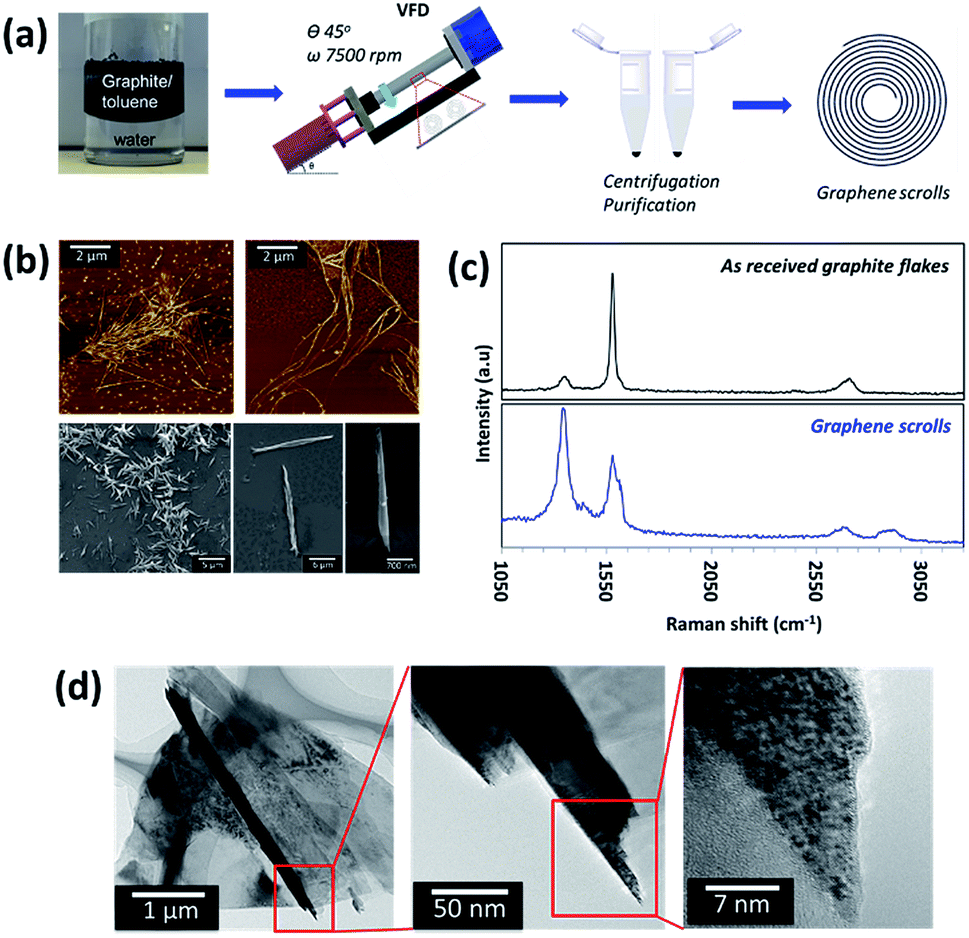 | ||
| Fig. 1 Schematic illustration and morphological characterization of the graphene scrolls. (a) Schematic illustration of the process for generating graphene scrolls in the VFD using a defined volume of toluene and water in a rapidly rotating 20 mm outer diameter (OD), 17.5 mm inner diameter (ID), borosilicate glass tube. (b) AFM phase images and SEM images of the graphene scrolls formed at a dispersed graphite concentration of 0.5 mg mL−1. (c) Raman spectra of the graphene scrolls and the as received graphite flakes, respectively, and (d) TEM and HRTEM characterization of an individual scroll revealing an average lattice spacing of 0.367 nm. | ||
A large number of the graphene scrolls were observed using AFM, SEM and TEM, confirming an average diameter of 151 ± 75 nm (measured at the central area of the scrolls) and an average length of 6.04 ± 4.0 μm. Some longer scrolls are present which may arise from entanglement of the graphene sheets during the scrolling/exfoliation process.9 The characteristic graphene fringes can be observed by HRTEM (Fig. 1). While these features can be attributed to MWCNTs, a number of lines of evidence suggest that the structures are indeed graphene scrolls. Firstly, HRTEM shows the structures to be open-ended. Secondly, SEM shows that the diameter of the tube is smaller at the two ends (Fig. 1b) which is consistent with the formation of scrolls (Fig. S5†). A third line of evidence comes from a control experiment of simultaneous irradiation of a pulsed Nd:YAG laser during the VFD processing.43,44 This is based on previous work, where we established the ability to laterally slice MWCNTs down to nanometer lengths by the combination of the shear forces in the VFD which bend the tube, and the laser irradiation, which ruptures the strained bonds. In the current work, the scroll structures were not sliced under these conditions, and thus is consistent with the suggestion that these tubular forms are indeed scrolls. The inability to laterally slice the graphene scrolls is due to it being harder to bend a rolled continuous sheet rather than concentric individual tubes (MWCNTs).
The energetics of the scrolling process was studied using atomistic modelling. Graphene scrolls were generated by mapping a graphene ribbon onto an Archimedean spiral with an interlayer distance of 3.35 Å and a prescribed inner radius, Ri (see insert (ii) in Fig. 2a). The potential energy profile for ribbons of five different lengths is shown in Fig. 2a. Tightly wrapped scrolls are unstable as the energy to curve them is greater than the energy gained from the van der Waals attraction. For larger inner radii, the van der Waals contribution decreases; once there is no overlapping of layers the potential energy becomes constant regardless of the inner radius. We compute the energy difference between the graphene ribbon and the optimally rolled scroll, V0. This quantity increases in magnitude with the scroll length (Fig. 2b) and in the infinite limit it approaches the energy difference between graphene and graphite, V∞. This limiting case, shown as a black dashed line, is the energy most relevant to the scrolls formed in the VFD as they contain many turns of a graphene sheet. To predict the temperature at which the scroll unravels, we constructed a Debye model of the phonon contribution to the total energy. According to the principle of equipartition, this energy is shared equally between the potential energy and the kinetic energy sub-systems; when the former exceeds V0 the scroll unravels. Fig. 2c shows the relationship between the Debye model potential energy (PE) component and temperature, predicting that unraveling will occur above 450 °C.
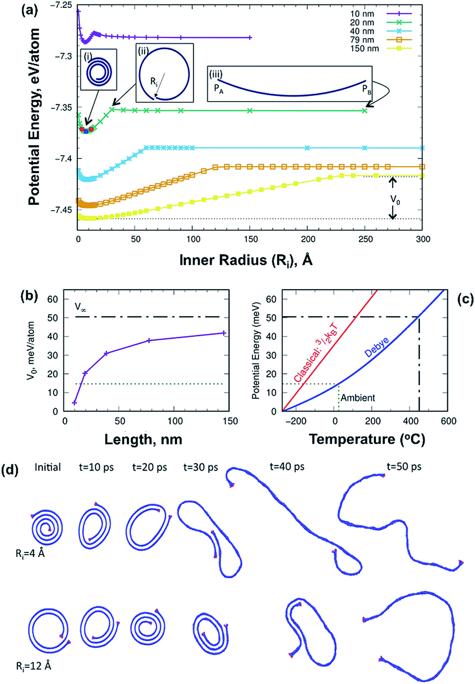 | ||
| Fig. 2 Atomistic calculations of the graphene scrolls. (a) Single-point energy for five scrolls of different lengths as a function of the inner radius. Insert (i) shows the structure of the 20 nm scroll for its optimal inner radius. Insert (ii) defines the inner radius parameter, Ri. Insert (iii) defines the length of the scroll as the distance between PA and PB. Dots indicate structures for which movies are provided (Fig. S6 in the ESI†). (b) Energy difference between the graphene ribbon and the scroll rolled at its optimal radius. The black dashed line indicates V∞, the energy difference between graphene and graphite. (c) Relationship between potential energy and temperature with a classical kinetic theory model and quantum mechanical Debye model, the latter predicting unravelling at 450 °C, as established experimentally. The green dotted line indicates the potential energy corresponding to ambient temperature, and (d) snapshots of scroll unravelling for a 20 nm long scroll. | ||
Thermostability of the scrolls was explored using thermogravimetric analysis (TGA) and differential scanning calorimetry (DSC) (Fig. 3a). The DSC (Fig. 3a red line) shows a thermodynamic response associated with a phase transition at 450 °C and it is marked with a red box in Fig. 3a. SEM images of the samples show that above this temperature the scrolls unravel, producing buckled graphene sheets as seen in Fig. 3b. This experimental threshold is in agreement with the theoretical model and provides strong evidence that the tubular structures are indeed scrolls. The TGA (Fig. 3a blue line) shows a small weight loss up to 200 °C associated with removal of toluene and water molecules physisorbed on the surface of the scrolls. There is a second weight loss that coincides with the phase transition which we interpret as the release of water and toluene molecules trapped in the core of the scrolls. The strongest evidence supporting the presence of scrolls is the fact that they unravel. If the structures were MWCNTs unravelling would require more aggressive treatment than just increasing the temperature. For example, longitudinal unzipping of MWCNTs has been reported by oxidation45 and by plasma etching;46 however these treatments result in graphene ribbons rather than crumpled graphene as seen herein.
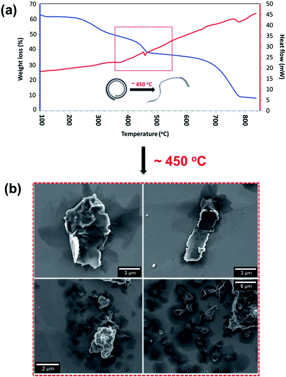 | ||
| Fig. 3 Thermal analysis of the graphene scrolls. (a) TGA and DSC with a 10 °C min−1 rate of temperature increase under N2. (b) SEM images of crumpled graphene sheets formed after heating the graphene scrolls at 500 °C. | ||
To examine the dynamics aspect of the unscrolling, we performed annealing simulations using molecular dynamics. Fig. 2d shows snapshots of the 20 nm long scroll for two inner radii. In the upper series, the initial scroll is tighter than the optimal value (0.756 nm), while in the lower series it is looser. In both cases the scroll unravels but the mechanism is different. The tightly wound scroll unravels continuously, while the other scroll first tightens to almost zero radius before unravelling. All the simulations show that the unscrolling does not occur in the manner of a carpet being laid down. Instead unscrolling always occurs by an expansion of the inner radius until the van der Waals attraction is lost. At this point the ribbon sometimes folds into a bilayer. Movies of the simulations can be found in the ESI.†
Before graphene derivatives can be used as electronic components several difficulties must be overcome, in particular, the high contact resistance between 2D graphene and metals.11,12 Recently there has been increased interest in using graphite as an electrode for making graphene come into contact with carbon nanotubes.12 Graphite has the advantage of being a bulk van der Waals material with an identical crystal structure to that of graphene. As a result, the contact interface, if aligned properly, can be made atomically smooth. In addition, graphite and graphene have similar work functions which should minimize contact doping that is responsible for the high resistance of metal–graphene contacts.47 Although only recent theoretical work has modelled electron transport across graphene–carbon structure junctions,13 the first experiments date back almost two decades, where conductive AFM of carbon nanotube–HOPG junctions was performed. In this work, it was shown that the resistance of the HOPG–carbon nanotube junctions has a strong dependence on the nanotube–graphite lattice angle which was explained by the periodic match/mismatch of the electron momentum between both the nanotube and graphite.48 Thus, in our work, we have tested the utility of graphene scrolls as an interface to connect to other graphene structures. For this purpose, we sandwiched individual graphene scrolls between a platinum AFM tip and HOPG which is one of the purest forms of graphite and its surface can well represent that of pristine graphene. The method employed is based on electrically wiring an individual graphene scroll using a platinum AFM tip, and simultaneously measuring the topography of an individual scroll while measuring the current passing between the tip and an HOPG electrode underneath under a constant force. This is performed using the peak force tunnelling AFM mode that provides direct control of the force applied via analysing individual force curves measured for a tip that is oscillating at a frequency significantly below the resonance frequency of the cantilever. While scanning in the x–y direction, a DC bias is applied between the tip and the surface of the HOPG electrode and the current passing between the tip and HOPG is recorded.
Fig. 4 shows the topographic image and the current map of the scrolls drop-cast on a HOPG electrode. A diluted drop casting solution was necessary to isolate individual scrolls of different dimensions. The topographical image (Fig. 4a) shows the typical background of HOPG with clear graphitic ribbons along with a group of the deposited graphene scrolls of different dimensions. The measured current was found to be higher when the AFM tip was in contact with the scrolls rather than when it was in contact with the bare HOPG. This is evident in the current maps (Fig. 4a and b) and in the current–voltage plots collected from the top of scrolls compared to that collected from bare HOPG (Fig. 5). It appears counterintuitive that by adding material (scrolls) and increasing the distance between the AFM tip and HOPG, the resistance of the junction decreases. However, an increase in the tip–substrate current is expected if the barrier for charge transport across the combined platinum–graphene scroll–HOPG junction is smaller than that in the background platinum–HOPG contact.
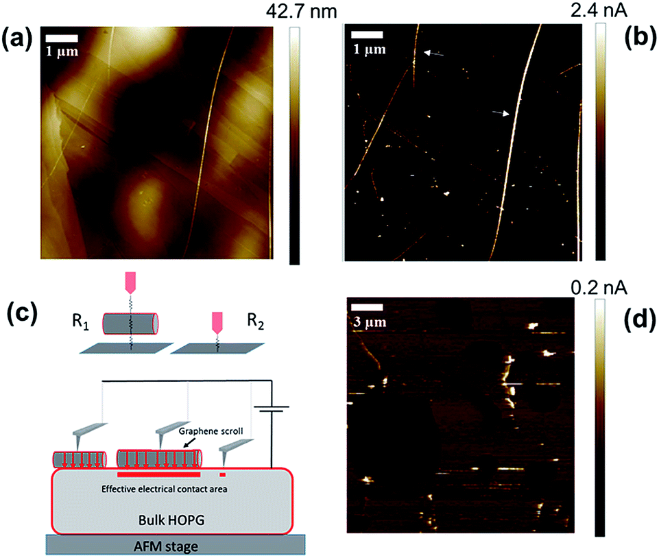 | ||
| Fig. 4 Peak force AFM. (a) Topography. (b) Current images taken at a sample bias of +100 mV. Arrows indicate individual graphene scrolls. Oscillation frequency was set to 1 kHz and the scan rate to 0.5 Hz. (c) Schematic diagram of the AFM tip–graphene scroll–HOPG junction. When the AFM tip is in contact with the bare HOPG, the current flows through one resistive component (R2), the direct contact between the platinum AFM tip and HOPG. However, when the AFM tip is positioned on the graphene scroll the current has to pass across three resistive components (R1) which include the interface between the platinum tip and the graphene scroll, the intrinsic resistance of the graphene scroll, and the resistance of the interface between the graphene scroll and HOPG. The larger the scrolls, the larger the effective contact area between the scroll and the HOPG, resulting in more current flowing through the tip–graphene scroll–HOPG junction, and (d) shows the current maps of graphite flakes assembled in a similar junction-configuration to that employed for the graphene scrolls. Unlike the junctions with graphene scrolls, the graphite junctions are more resistive than the bare contact with the HOPG electrode. | ||
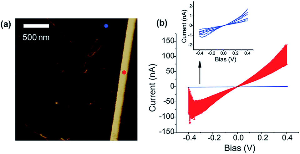 | ||
| Fig. 5 Current–potential relationship of the graphene scrolls compared to that of bare HOPG. (a) AFM height image of a graphene scroll. (b) The corresponding current–potential curves measured on the scrolls (red colour) and on the background HOPG (blue colour). The I–V sampling locations are indicated with red and blue dots. | ||
The resistance of the junction formed with a graphene scroll can be described as R1 = Rplatinum/graphene scroll + Rgraphene scroll + Rgraphene scroll/HOPG. On the other hand, the bare platinum contact with HOPG will have only one, but a different resistive component R2 = Rplatinum/HOPG. Higher currents are produced when the tip is in contact with the graphene scroll, and this means that the series of resistances summed in R1 is smaller than that produced by the platinum/HOPG contact (R2). This can be explained by the following: first, the charge injection between the platinum and the graphene scroll is higher than that between the platinum and the bare HOPG. Second, the intrinsic resistivity of the graphene scrolls is lower than that of the surface of HOPG. This is attributed to the graphene scrolls being a single layer of graphene and not a topologically closed structure. Hence, intercalation with solvents is likely to occur between the rolls within a scroll; this is in contrast with other cylindrical structures of carbon such as MWCNTs which resist lattice expansion due to intercalation. We speculate that such an expansion in the lattice of the graphene scrolls can make the scrolls better resemble free-standing graphene of higher electron mobility, increasing its conductivity over graphene layers that are tightly packed or interacting with the surface. Finally, the resistance between HOPG and graphene scrolls is very low, and this can be explained by the scrolls and HOPG having atomically smooth lattices at the contact region. In addition to a smooth contact, both HOPG and the scrolls have similar work functions and therefore energy-level alignment can occur at the HOPG–scroll interface. This is supported by the observed increase in current, and decrease in resistance, when the HOPG contact was made with larger scrolls, which necessarily increases the contact area, enabling more current flow. The highly conducting junction of the graphene scroll interface is in contrast to that formed with graphite flakes (Fig. 4d), the starting material from which the scrolls were made. In the latter the junctions are more resistive than that formed with the bare HOPG. We attribute this higher resistance to the irregular geometry at the contact of the graphite flakes and HOPG and to the intrinsic resistivity of pristine graphite flakes. Although electron transmission calculations will be needed to better understand graphene scroll–graphite junctions, we have demonstrated that the electrical contact to HOPG is substantially improved using a graphene scroll interfacial layer. It can be envisioned that these observations will assist in the design and understanding of graphene circuitry.
Conclusions
We have developed a facile one-step method of fabricating graphene scrolls, which are formed under shear stress generated within dynamic thin films in a vortex fluidic device. The stable graphene scrolls (<450 °C) were produced in high yield following recycling through the microfluidic platform, in the absence of auxiliary surfactants, or other chemicals, and with minimal processing times. Scaling up of the process is possible using a parallel array of VFDs, coupled with recycling of residual graphite, or the use of a large VFD, but here a necessary understanding of the fluid dynamics up front will be a major challenge. The fabricated scrolls showed low contact resistance when interfaced with other forms of graphene, such as the surface of HOPG electrodes, as evidenced by current sensing atomic force microscopy. These properties pave the way for new applications of graphene multilayers as electrical conduits in all sp2 organic circuitry. The graphene scrolls are also foreseen to show explicit potential in a number of fields, with the accessibility to be readily scaled up.Conflicts of interest
There are no conflicts to declare.Acknowledgements
The authors gratefully acknowledge support of this work by the Australian Research Council (DP170100450) and the Government of South Australia. The authors also acknowledge the expertise, equipment and support provided by the Australian Microscopy and Microanalysis Research Facility (AMMRF) and the Australian National Fabrication Facility (ANFF) at the South Australian nodes of the AMMRF and ANFF under the National Collaborative Research Infrastructure Strategy. N. D. acknowledges an ARC-DECRA fellowship – DE160101101.References
- C. Lee, X. Wei, J. W. Kysar and J. Hone, Science, 2008, 321, 385–388 CrossRef CAS PubMed.
- R. S. Edwards and K. S. Coleman, Nanoscale, 2013, 5, 38–51 RSC.
- M. J. Allen, V. C. Tung and R. B. Kaner, Chem. Rev., 2012, 110, 132–145 CrossRef.
- S. Stankovich, D. A. Dikin, G. H. B. Dommett, K. M. Kohlhaas, E. J. Zimney, E. A. Stach, R. D. Piner, S. T. Nguyen and R. S. Ruoff, Nature, 2008, 442, 282–286 CrossRef PubMed.
- J. S. Bunch, A. M. van der Zande, S. S. Verbridge, I. W. Frank, D. M. Tanenbaum, J. M. Parpia, H. G. Craighead and P. L. McEuen, Science, 2007, 315, 490–493 CrossRef CAS PubMed.
- P. Blake, P. D. Brimicombe, R. R. Nair, T. J. Booth, D. Jiang, F. Schedin, L. A. Ponomarenko, S. V. Morozov, H. F. Gleeson, E. W. Hill, A. K. Geim and K. S. Novoselov, Nano Lett., 2008, 8, 1704–1708 CrossRef.
- Y. Zhang, Y. W. Tan, H. L. Stormer and P. Kim, Nature, 2007, 438, 457–460 Search PubMed.
- M. D. Stoller, S. Park, Y. Zhu, J. An and R. S. Ruoff, Nano Lett., 2008, 8, 3498–3502 CrossRef CAS PubMed.
- N. Liu, A. Chortos, T. Lei, L. Jin, T. R. Kim, W. G. Bae, C. Zhu, S. Wang, R. Pfattner, X. Chen, R. Sinclair and Z. Bao, Sci. Adv., 2017, 3(9), e1700159 CrossRef PubMed.
- Z. Liu, J. Wang, H. Ding, S. Chen, X. Yu and B. Lu, ACS Nano, 2018, 12, 8456–8466 CrossRef CAS PubMed.
- L. Wang, I. Meric, P. Y. Huang, Q. Gao, Y. Gao, H. Tran, T. Taniguchi, K. Watanabe, L. M. Campos, D. A. Muller, J. Guo, P. Kim, J. Hone, K. L. Shepard and C. R. Dean, Science, 2013, 342, 614–617 CrossRef CAS PubMed.
- T. Chari, R. Ribeiro-Palau, C. R. Dean and K. Shepard, Nano Lett., 2014, 16, 4477–4482 CrossRef PubMed.
- P. T. Robert and R. Danneau, New J. Phys., 2014, 16, 013019 CrossRef.
- F. Jovell and X. Cartoixa, J. Phys.: Condens. Matter, 2018, 30, 325302 CrossRef PubMed.
- I. Suarez-Martinez, N. Grobert and C. P. Ewels, Carbon, 2012, 50, 741–747 CrossRef CAS.
- X. Chen, R. A. Boulos, T. F. Dobson and C. L. Raston, Nanoscale, 2013, 5, 498–502 RSC.
- F. Zeng, Y. Kuang, G. Liu, R. Liu, Z. Huang, C. Fu and H. Zhou, Nanoscale, 2012, 4, 3997–4001 RSC.
- K. Yao, M. Manjare, C. A. Barreett, B. Yang, T. T. Salguero and Y. Zhao, J. Phys. Chem. Lett., 2012, 3, 2204–2208 CrossRef CAS PubMed.
- F. Zeng, Y. Kuang, Y. Wang, Z. Huang, C. Fu and H. Zhou, Adv. Mater., 2011, 23, 4929–4932 CrossRef CAS PubMed.
- C. A. Amadei, I. Y. Stein, G. J. Silverberg, B. L. Wardle and C. D. Vecitis, Nanoscale, 2016, 8, 6783–6791 RSC.
- X. Xie, L. Ju, X. Feng, Y. Sun, R. Zhou, K. Liu, S. Fan, Q. Li and K. Jiang, Nano Lett., 2009, 9, 2565–2570 CrossRef CAS PubMed.
- L. M. Viculis, J. J. Mack and R. B. Kaner, Science, 2003, 299, 1361 CrossRef CAS PubMed.
- B. Tang, Z. Xiong, X. Yun and X. Wang, Nanoscale, 2018, 10, 4113–4122 RSC.
- L. Wang, P. Yang, Y. Liu, X. Fang, X. Shi, S. Wu, L. Huang, H. Li, X. Huang and W. Huang, Nanoscale, 2017, 9, 9997 RSC.
- Y. Liu, L. Wang, H. Zhang, F. Ran, P. Yang and H. Li, RSC Adv., 2017, 7, 40119 RSC.
- T. M. D. Alharbi, D. Harvey, I. K. Alsulami, N. Dehbari, X. Duan, R. N. Lamb, W. D. Lawrance and C. L. Raston, Carbon, 2018, 137, 419–424 CrossRef CAS.
- L. Gao, Z. Zhang, J. Zhao, J. Zhou, Z. Miao, W. Si and S. Zhuo, RSC Adv., 2018, 8, 19164–19170 RSC.
- D. Y. Hwang, J. Y. Yook and D. H. Suh, RSC Adv., 2014, 4, 35943–35949 RSC.
- G. Mpourmpakis, E. Tylianakis and G. E. Froudakis, Nano Lett., 2007, 7, 1893–1897 CrossRef CAS PubMed.
- V. R. Coluci, S. F. Braga, R. H. Baughman and D. S. Galvao, Phys. Rev. B: Condens. Matter Mater. Phys., 2007, 75, 12504 CrossRef.
- X. Yang, Y. S. He, G. Jiang, X. Z. Liao and Z. F. Ma, Electrochem. Commun., 2011, 13, 1166–1169 CrossRef CAS.
- L. Yasmin, X. Chen, K. A. Stubbs and C. L. Raston, Sci. Rep., 2013, 3, 2282 CrossRef PubMed.
- J. Britton, K. A. Stubbs, G. A. Weiss and C. L. Raston, Chem.–Eur. J., 2017, 23, 13270–13278 CrossRef CAS PubMed.
- K. Vimalanathan, X. Chen and C. L. Raston, Chem. Commun., 2014, 50, 11295–11298 RSC.
- X. Chen, J. F. Dobson and C. L. Raston, Chem. Commun., 2012, 48, 3703–3705 RSC.
- K. Vimalanathan, R. G. Shrestha, Z. Zhang, J. Zou, T. Nakayama and C. L. Raston, Angew. Chem., Int. Ed., 2017, 56, 8398–8401 CrossRef CAS PubMed.
- I. K. Alsulami, T. M. D. Alharbi, D. P. Harvey, C. T. Gibson and C. L. Raston, Chem. Commun., 2018, 54, 7896–7899 RSC.
- F. Tunistra and J. L. Koenig, J. Chem. Phys., 1970, 53, 1126–1130 CrossRef.
- G. Carotenuto, A. Longo, S. D. Nicola, C. Camerlingo and L. Nicolais, Nano Lett., 2013, 8, 403 CrossRef PubMed.
- J. Zheng, H. Liu, B. Wu, Y. Guo, T. Wu, G. Yu, Y. Liu and D. Zhu, Adv. Mater., 2011, 23, 2460–2463 CrossRef CAS PubMed.
- D. Roy, E. A. Tactay, R. J. C. Brown, S. J. Spencer, T. Fry, T. A. Dunton, T. Young and M. J. T. Milton, Chem. Phys. Lett., 2008, 465, 254–257 CrossRef CAS.
- H. Q. Zhou, C. Y. Qiu, H. C. Yang, F. Yu, M. J. Chen, L. J. Hu, Y. J. Guo and L. F. Sun, Chem. Phys. Lett., 2011, 501, 475–479 CrossRef CAS.
- K. Vimalanathan, J. R. Gascooke, I. Suarez-Martinez, N. A. Marks, H. Kumari, C. J. Garvey, J. L. Atwood, W. D. Lawrance and C. L. Raston, Sci. Rep., 2016, 6, 22865 CrossRef CAS PubMed.
- T. M. D. Alharbi, K. Vimalanathan, W. D. Lawrance and C. L. Raston, Carbon, 2018, 140, 428–432 CrossRef CAS.
- D. V. Kosynkin, A. L. Higginbotham, A. Sinitskii, J. R. Lomeda, A. Dimiev, B. K. Price and J. M. Tour, Nature, 2009, 458, 872–876 CrossRef CAS PubMed.
- L. Jiao, L. Zhang, X. Wang, G. Diankov and H. Dai, Nature, 2009, 458, 877–880 CrossRef CAS PubMed.
- J. T. Smith, A. D. Franklin, D. B. Farmer and C. D. Dimitrakopoulos, ACS Nano, 2013, 7, 3661–3667 CrossRef CAS PubMed.
- S. Paulson, A. Helser, M. B. Nardelli, R. M. Taylor II, M. Falvo, R. Superfine and S. Washburn, Science, 2000, 290, 1742–1744 CrossRef CAS PubMed.
Footnote |
| † Electronic supplementary information (ESI) available: See DOI: 10.1039/c9na00184k |
| This journal is © The Royal Society of Chemistry 2019 |