 Open Access Article
Vapor growth of binary and ternary phosphorus-based semiconductors into TiO2 nanotube arrays and application in visible light driven water splitting†
Ebru
Üzer
 a,
Pawan
Kumar‡
 b,
Ryan
Kisslinger‡
b,
Piyush
Kar
b,
Ujwal Kumar
Thakur
b,
Karthik
Shankar
b,
Ryan
Kisslinger‡
b,
Piyush
Kar
b,
Ujwal Kumar
Thakur
b,
Karthik
Shankar
 *b and
Tom
Nilges
 *a
*a
aDepartment of Chemistry, Technical University of Munich, Lichtenbergstr. 4, 85748 Garching, Germany. E-mail: tom.nilges@lrz.tum.de
bDepartment of Electrical and Computer Engineering, 9211-116 Street NW, Edmonton, Alberta, Canada T6G 1H9. E-mail: kshankar@ualberta.ca
First published on 24th May 2019
Abstract
We report successful synthesis of low band gap inorganic polyphosphide and TiO2 heterostructures with the aid of short-way transport reactions. Binary and ternary polyphosphides (NaP7, SnIP, and (CuI)3P12) were successfully reacted and deposited into electrochemically fabricated TiO2 nanotubes. Employing vapor phase reaction deposition, the cavities of 100 μm long TiO2 nanotubes were infiltrated; approximately 50% of the nanotube arrays were estimated to be infiltrated in the case of NaP7. Intensive characterization of the hybrid materials with techniques including SEM, FIB, HR-TEM, Raman spectroscopy, XRD, and XPS proved the successful vapor phase deposition and synthesis of the substances on and inside the nanotubes. The polyphosphide@TiO2 hybrids exhibited superior water splitting performance compared to pristine materials and were found to be more active at higher wavelengths. SnIP@TiO2 emerged to be the most active among the polyphosphide@TiO2 materials. The improved photocatalytic performance might be due to Fermi level re-alignment and a lower charge transfer resistance which facilitated better charge separation from inorganic phosphides to TiO2.
1. Introduction
Depleting fossil fuel reserves and rising atmospheric greenhouse gas concentration have motivated the search for new energy sources. Using sunlight as the energy source to generate hydrogen from water through water splitting is an enticing approach. Hydrogen is considered a clean fuel with a high calorific value; it can be stored in a solid/liquid adsorbent or transformed into hydrocarbons using CO2 to produce a syngas mixture. Many photocatalytic materials such as ZnO, CdS, ZnS, InVO4, AgPO4, SrTiO3 and TaON have been widely investigated to achieve water splitting.1–4 TiO2 has proven to be an excellent photocatalytic material due to its promising band edge potential, non-toxic and non-corrosive nature, and earth-abundance. However, issues such as its large band gap, less reductive conduction band, short lived charged carriers and poor quantum efficiency are the main obstacles preventing the successful deployment of sustainable photocatalysts.5–7 Hybridization of TiO2 with various low band gap semiconductors to produce direct/Z-scheme photocatalysts, doping, sensitization, formation of Schottky junctions and nanoscale structural modification (i.e., nanotubes/nanorods/nanospikes/nanospheres) have proven to enhance photocatalytic performance and/or charge separation.8–13 Polyphosphides are an intriguing class of low band gap semiconductors for this purpose.14,15 We selected three polyphosphides, namely NaP7, SnIP (ranging from 1.71–1.86 eV)16–18 and (CuI)3P12 (2.84 eV, own measurement see below) because of their different band gaps and their ability to be synthesized in a mineralizer-assisted transport reaction.19,20 NaP7, a 2 eV-semiconductor material, plays a crucial role in the sodification and desodification processes in sodium ion batteries.18 SnIP represents the first inorganic atomic-scale-double helix compound and (CuI)3P12 is an adduct phase from CuI and a neutral phosphorus chain.21–23TiO2 nanotubes are hollow nano-sized cylinders that form in vertically oriented arrays over large areas on the underlying substrate. The nanotubes are fabricated by electrochemical anodization of Ti films or foil in electrolytes typically containing F− through the simultaneous occurrence of field-assisted Ti oxidation, field-assisted dissolution of Ti and TiO2, and chemical dissolution of TiO2.24,25 The as-synthesized nanotubes are amorphous and are crystallized to n-type semiconducting anatase either by annealing in air at temperatures of 350–550 °C or by a hydrothermal treatment at lower temperatures.26,27 TiO2 nanotubes exhibit remarkable versatility in the type of substrate they can be grown on, having been demonstrated on Si, ITO-coated glass, FTO-coated glass, quartz, polyimide and Ti foil, and also as free-standing membranes.28–30 Likewise, the nanotube diameter can be varied over a wide range (10 to 900 nm).31,32 These characteristics make TiO2 nanotubes ideal for the templated growth of inorganic phosphorus-based semiconductors through diffusive chemical vapor transport into the nanotube pores at elevated temperatures.
While electrodeposition and chemical vapor deposition into nanoporous anodic aluminium oxide (AAO) templates have been previously used to form nanorods and nanofibers of CdS, CdSe, Si, Bi, etc. exhibiting quantum confinement effects,33–36 the application spectrum for semiconductor nanowires formed by chemical vapor transport deposition into anodic TiO2 nanotube arrays is much greater. This is because the TiO2 nanotubes are n-type semiconductors (charge carrier density ∼1018 to 1019 cm−3)37 and allow the formation-in-place of a semiconductor heterojunction while AAO is an insulator, precluding the formation of a useful heterojunction. Furthermore, for a heterojunction to be electronically useful in applications that rely on light harvesting (photodetectors, photovoltaics, photocatalysts, and photoelectrochemical sensors) it is essential for excess carriers to be efficiently separated and for photons to be completely harvested. In this regard, vertically oriented nanotubes and nanowires are uniquely suited because the processes of charge separation and light absorption are orthogonalized.38 Charge carriers created in a semiconductor nanorod formed inside the nanotubes need to merely travel a distance equal to the nanotube radius before encountering a heterojunction interface for charge separation while the high aspect ratio of the nanotubes ensures that even weakly absorbed photons are harvested. Furthermore, light trapping effects such as photonic crystals and resonant Mie scattering can be easily incorporated into the nanotubes to increase their photonic strength.32,39 Indeed, heterojunctions of TiO2 nanotubes with solution-processed semiconductors such as CdS, CdSe, PbS, Fe2O3, Cu2ZnSnS4, g-C3N4, halide perovskites, etc. have been used to demonstrate efficient Z-scheme CO2 reduction photocatalysts,40 high performance water photolyzers,41 selective gas sensors,42 and high efficiency solar cells.43,44 Herein, we introduce TiO2–polyphosphide heterojunctions consisting of polyphosphide nanofibers formed by the hitherto unexplored process of chemical vapor transport into TiO2 nanotube array templates.
2. Results and discussion
Section 2.1 describes the synthesis of the TiO2 nanotubes and nanohybrids in brief. Sections 2.2 and 2.3 describe our characterization of NaP7@TiO2 and SnIP@TiO2 heterostructures. Following the same principle as that for NaP7 and SnIP, the synthesis, characterization and physical property measurement details of (CuI)3P12 on TiO2 heterostructures are circumstantiated, as well as a full description of all synthesis parameters and characterization techniques in the ESI Section.† Section 2.4 and 2.5 summarize X-ray Photoelectron Spectroscopy (XPS) and UV-Vis studies of the heterostructures, with details given in the ESI† respectively. Section 2.6 deals with photocatalytic activity measurements and related characterization. Detailed interface photon-to-current efficiency performance as well as semiconductor–electrolyte interface analysis are described in the ESI† as well as sections on Electrochemical Impedance Spectroscopy (EIS), impedance-potential measurements, and Kelvin Probe Force Microscopy (KPFM).2.1 Synthesis of polyphosphide@TiO2 nanotube hybrids
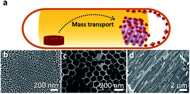
A low-cost and easily accessible method to fabricate nanostructured photochemically active hybrid poly-phosphide@TiO2 heterostructures has been developed following a short-way transport reaction onto and into electrochemically fabricated TiO2 nanotube membranes (Fig. 1). Synthesis details are given in the ESI.†2.2 NaPx@TiO2 nanotubes
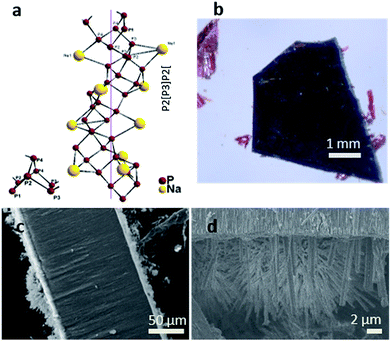
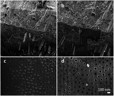
Fig. 2a displays the crystal structure of NaP7 and a representative membrane after the gas phase deposition reaction is shown. Small crystals of NaP7 were formed on the surface of the TiO2 membrane (see Fig. 2b). A Scanning Electron Microscopy (SEM) image of the TiO2 membrane cross section substantiates the growth of NaP7 on both sides of the membrane. It is obvious from Fig. 2c that the crystal sizes are different on both sides which directly correlates with the TiO2 nanotube pore width on either side. The cross-sectional images were taken after cutting the polyphosphides@TiO2 nanotubes with a razor, taking the images along the cut edges. Obviously, the growth of the polyphosphide crystals started from the surface or even from inside the TiO2 nanotube directly into the gas phase (see Fig. 3). Therefore, many crystals are grown straight out of the nanotubes. A second hint for a growth from the inside into the gas phase might be the differences in the sizes of the crystals on both sides of the membrane (corresponding SEM data in Table S1†). On the other hand, the size of the TiO2 nanotubes can directly define the diameter of the resulting NaPx crystals (x = 7, 15).Two visually different main fractions lying on the top and bottom of the TiO2 membrane sides were observed. The samples were manually separated, and data collection of powder X-ray diffraction led to a nearly phase pure pattern of NaP7 (main fraction) and a diffraction pattern of NaP15 (minor fraction) reflecting distinct texture effects (see S1a and b). To verify the assumption that a significant transport of the material occurred via the gas phase to the inside of the nanotubes, we examined the cross section of a broken membrane by position-sensitive EDS scans (Table S1†). The data along the cross section of the membrane show a constant Na![[thin space (1/6-em)]](https://www.rsc.org/images/entities/char_2009.gif) :
:![[thin space (1/6-em)]](https://www.rsc.org/images/entities/char_2009.gif) P ratio of approx. 1
P ratio of approx. 1![[thin space (1/6-em)]](https://www.rsc.org/images/entities/char_2009.gif) :
:![[thin space (1/6-em)]](https://www.rsc.org/images/entities/char_2009.gif) 9 towards the top side view of the membranes (larger holes), where the crystals on the surface show a larger size and a ratio of 1
9 towards the top side view of the membranes (larger holes), where the crystals on the surface show a larger size and a ratio of 1![[thin space (1/6-em)]](https://www.rsc.org/images/entities/char_2009.gif) :
:![[thin space (1/6-em)]](https://www.rsc.org/images/entities/char_2009.gif) 4 towards the bottom side of the membranes (smaller holes), where the crystals show a smaller size. This finding substantiates our hypothesis that Na and P were transported into the TiO2 nanotubes along a certain length of the membrane. To verify the filling grade of the nanotubes, and therefore the efficiency of the gas phase transport, a FIB experiment was performed on a selected spot of the membrane. The FIB was used to cut off the upper part down to 15 nm of the membrane to facilitate an observation of the nanotube's subsurface. We found non-filled and filled tubes on the area we treated (see Fig. 3). Taking a closer look at the tubes, a filling grade of 50% can be estimated from the FIB pictures.
4 towards the bottom side of the membranes (smaller holes), where the crystals show a smaller size. This finding substantiates our hypothesis that Na and P were transported into the TiO2 nanotubes along a certain length of the membrane. To verify the filling grade of the nanotubes, and therefore the efficiency of the gas phase transport, a FIB experiment was performed on a selected spot of the membrane. The FIB was used to cut off the upper part down to 15 nm of the membrane to facilitate an observation of the nanotube's subsurface. We found non-filled and filled tubes on the area we treated (see Fig. 3). Taking a closer look at the tubes, a filling grade of 50% can be estimated from the FIB pictures.
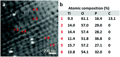
To determine the filling elemental depth profile, the FIB milled area (shown in Fig. 4) was analysed via Auger electron spectroscopy (AES) and microscopy (see Fig. 4 and AES spectra in Fig. S2†). Fig. 4a shows locally analysed FIB-milled spots with spot 1 demonstrating the analysis of a tube considered empty; notably, it is the only spot indicating the presence of carbon. Due to sample cleaning by argon ion bombardment, it is assumed that carbon has been cleaned off, as it is not present in all other spots but spot 1 being inaccessible to cleaning and therefore showing the presence of C. Spots 2–6 have much higher P contents than spot 1 even after deducting the C content (a proportionate rise of P to 18.9 at%). This suggests that the spot 2–6 nanotubes were filled, while the spot 1 tube was not; the signal at spot 1 of P is not attributed to the P content in the apparently empty nanotube but appears due to the approximately 10 nm resolution of the instrument. The most prominent Na peaks appear at 24 eV (Na KLL, overlap in AES spectra, Fig. S2†) and taking the relatively low Na to P ratio into account, a merely weak peak at 979 eV (Na LVV).
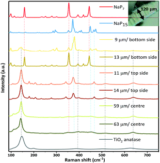
Raman spectroscopy on the surface and cross section of a membrane (cut apart with a razor) was carried out to validate the successful transport of the material into the TiO2 nanotube membranes. We measured the depth of intake of a material by moving the Raman laser gradually along the cross section, acquiring spectra at specific spots. The laser has a standard mode spot size of 1.5 microns (at 50× magnification). From a series of spectra recorded at different depths and from both sides of the membrane, we found the penetration of NaPx through the whole membrane. Raman spectra recorded along the cross section at several distances from the surface suggest two additional phases next to TiO2 anatase after gas phase synthesis together with the nanotube membranes. The most prominent modes at 352 cm−1 (NaP7) and 377 cm−1 (NaP15) of the Raman data show the simultaneous presence of NaP7 at 9 μm and NaP15 at 13 μm distance from the bottom side of the membrane surface next to a signal at 145 cm−1 for TiO2 anatase (Eg) (Fig. 5). By recording along the tube length characteristic signals of less intensity confirm the presence in the centre of the nanotubes up to the top membrane side, where NaP15 can be found at 11 and 14 μm deep into the surface. Obviously, the crystallinity was significantly reduced going deeper into the membrane.
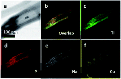
Representative single TiO2 nanotubes were separated from a membrane by an ultrasonication step and STEM imaging and EDS mapping was performed to corroborate the filling of the tubes with NaPx, as shown in Fig. 6. Na and P were detected along the full tube length. CuI was used as a transport agent and can be displayed in the elemental analysis in significant amounts. Cu was only present in defined crystals attached to the membranes and it could not be detected in reasonable amounts inside the tubes. Such defined crystals are possibly formed during the transport process as side phases or represent the remaining transport agent.
The chemical vapor deposition of NaP7 and NaP15 phases onto TiO2 nanotube membranes can be verified via powder XRD patterns. As SEM-EDS data show, the nanotubes are filled from both sides with NaPx phases. This can be further proved by EDS- and Auger-results after FIB-milling into a depth of about 200 nm of the membranes. Raman spectra recorded at the center of the membrane cross section after synthesis show signals in the ranges of NaP7 and NaP15 modes next to the anatase phase. After an ultrasonication process, Scanning Transmission Electron Microscopy-Energy-dispersive X-ray Spectroscopy (STEM-EDS) measurements show furthermore the presence of Na, P and Cu of the transport agent within the single tubes.
2.3 SnIP@TiO2 nanotubes
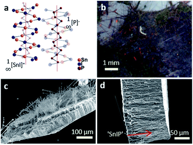
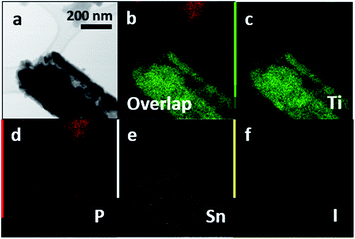
We have further substantiated the chemical vapor deposition of the inorganic double helical semiconductor SnIP featuring a band gap of 1.86 eV on TiO2 nanotube arrays (see Fig. 7a).17 SnIP is anticipated to be formed from the gaseous phases of the precursors and a comproportionation reaction of Sn and SnI4 to SnI2. Therefore, no additional mineralizer was needed to cover the surface of the TiO2 nanotube membranes with SnIP as depicted in the microscopy images in Fig. 7b and c. The SEM image substantiates the growth of SnIP on the nanotube, when detecting the elemental composition via EDS measurements. The detection of Sn and I was diminished going further into the tubes (Table S2†). A possible explanation is that during the transport reaction through a gas phase the formation of pure phosphorus species deeper in the nanotubes can be more likely than the double helical structure of 1∞[SnI+]– and 1∞[P−]–chains. Powder X-ray diffraction verifies the formation of crystalline SnIP on the TiO2 membranes (Fig. S3†).STEM imaging after the separation of the TiO2 nanotubes by an ultrasonication process shows a set of nanotubes with a size of ∼80–100 nm per tube. Elemental mapping confirms Ti (representing TiO2), P, Sn, and I with a distribution of P along the tube length. Sn and I appear to be present in smaller amounts in a TiO2 tube (Fig. 8).
SnIP was grown successfully onto and into TiO2 nanotube arrays via a gas phase as verified using powder X-ray diffraction and SEM-EDS. The transportation of the ternary compounds into the nanotubes was demonstrated with STEM-EDS analysis.
2.4 XPS studies
We performed XPS studies on the pure semiconductors NaPx, SnIP and (CuI)3P12 and the three semiconductor@TiO2 nanotube heterostructures in order to verify the surface compositions, binding energies and oxidation states of the materials (Fig. S7–S9 and Table S6†). All oxidation states in the heterostructure systems are consistent with the ones observed for the pure compounds along with surface oxidized phosphates (PxOy). In the case of (NaP7, NaP15)@TiO2 we found a shift of the Na1s peak in NaP7@TiO2 to higher binding energy which might be due to partial charge transfer from NaP7 to the surface of TiO2 and doping of the TiO2 surface with Na+ ions to some extent. The peak positions of Ti and O remained unchanged upon semiconductor loading into the tubes (Fig. S7†). A comparable charge transfer behaviour was observed for the (CuI)3P12@TiO2 heterostructure compound (see Fig. S8†).XPS spectra of SnIP@TiO2 do not show any significant change of the Sn, I and P peaks which we interpret as the absence of significant bonding interaction between the two phases (shown in Fig. S9†).
2.5 UV-Vis spectra
The absorption properties of materials in the UV-Vis region were determined by diffuse reflectance UV-Vis spectroscopy (Fig. S6a†). The absorption spectra of TiO2 nanotubes show an intense band at 330 nm with band tailing up to 384 nm, which corresponds to a valence band to conduction band (O2p → Ti3d) transition.45,46 The UV-Vis spectra of NaP7 displayed broad absorption in the visible region extended up to 800 nm, which is attributed to charge generation in the phosphide chain motif. The NaP7@TiO2 heterostructures displayed an absorption band which corresponded to TiO2 along with an absorption profile in the visible region due to the presence of NaP7. Pristine SnIP displayed a broad absorption edge up to 700 nm which is shifted up to 500 nm in SnIP@TiO2, with a slight increase in the absorption profile at higher wavelengths (Fig. S10†). The UV-Vis spectra of pristine (CuI)3P12 show an intense absorption edge extended up to 440 nm which is slightly decreased in (CuI)3P12@TiO2 samples (Fig. S10†). To probe the visible light absorption of the samples, the optical band gap of each material was determined using a Tauc plot by plotting a graph of (αhν)1/2vs. hν followed by extrapolation of a linear tangent to the abscissa, where α is the absorption coefficient, h is the Planck constant, and ν is the light frequency (Fig. S10†). The band gaps for TiO2, NaP7, NaP7@TiO2, SnIP, SnIP@TiO2, (CuI)3P12 and (CuI)3P12@TiO2 (see Table 1) are in close agreement with reported values. Due to the band gap values a certain absorption in the visible light region is present (Fig. S6†).| Sample | Band gap [eV] | Photocurrent density [mA cm−2] | Max ABPE [%] | IPCE [%] | APCE [%] |
|---|---|---|---|---|---|
| TiO2 | 3.05 | 0.21 | 0.07 | 0.007 | 0.01 |
| NaP7 | 1.28 | 0.20 | 0.04 | 0.04 | 0.06 |
| NaP7@TiO2 | 1.87 | 0.22 | 0.05 | 0.36 | 0.43 |
| SnIP | 1.84 | 0.20 | 0.02 | 2.0 | 0.46 |
| SnIP@TiO2 | 2.22 | 0.84 | 0.20 | 0.20 | 3.2 |
| (CuI)3P12 | 2.84 | 0.41 | 0.06 | 0.46 | 0.78 |
| (CuI)3P12@TiO2 | 2.73 | 0.43 | 0.09 | 0.48 | 1.19 |
2.6 Photocatalytic activity measurement
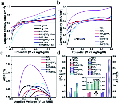
The photocatalytic performance of the hybrid materials was discerned by photoelectrochemical water splitting experiments. A three-electrode configuration was used, composed of pristine/hybrid materials deposited on FTO glass as the photoanode, Pt as the cathode and Ag/AgCl as the reference electrode, all immersed in a 0.1 M KOH electrolyte. The photoanode was irradiated with AM1.5 G solar simulated light having a power density of 100 mW cm−2 on the surface of the sample. The photocurrent density per cm2 was measured in linear sweep voltammetry (LSV) mode by switching the applied bias from −1.0 V to +0.8 V vs. Ag/AgCl. The dark current was also measured to compare the photoelectrochemical response. At an applied bias of 0.6 V vs. Ag/AgCl (1.23 V vs. RHE which is the water oxidation potential), the photocurrent density values of TiO2, NaP7, NaP7@TiO2, SnIP, SnIP@TiO2, (CuI)3P12 and (CuI)3P12@TiO2 are shown in Table 1. Under dark conditions the current density remains almost zero, while after irradiation under solar simulated light bare TiO2 shows extremely low photocurrent (0.21 mA cm−2) which is in good agreement with its large band gap (∼3.2 eV), as shown in Fig. 9a. Similarly, the photocurrent density for bare NaP7, (CuI)3P12 and SnIP remained low due to the inability of poorly oxidative holes to facilitate water splitting. Thus, the order of performance is SnIP > (CuI)3P12 > NaP7. Furthermore, the hybrids NaP7@TiO2 and (CuI)3P12@TiO2 also displayed a small improvement in photocatalytic performance over the pristine phosphide material which might be due to unfavourable Fermi level alignment resulting in sluggish charge separation. However, hybrids of SnIP phosphides with TiO2 (SnIP@TiO2) demonstrated a much higher photocurrent density (0.82 mA cm−2) than individual components and NaP7@TiO2 and (CuI)3P12@TiO2; this suggests the formation of a heterojunction and feasible transfer of electrons and holes. The higher photocurrent for SnIP@TiO2 is attributed to better coverage of the TiO2 surface by SnIP and more long-range ordering of the SnIP helix which facilitates faster charge injection into the conduction band of TiO2. To validate the photoresponse of materials, the photocurrent was measured during a light on–off cycle, which clearly demonstrated the materials' photo-responsive nature (Fig. S11†). Furthermore, the ability to drive water splitting at longer wavelengths was proved by measuring the photocurrent response of the materials under 425 nm and 505 nm wavelength light irradiation having a power density of 54.15 and 40.48 mW cm−2, respectively, at the surface of the samples (Fig. 9b). Again, the highest photocurrent density (0.32 mA cm−2 at 450 nm and 0.34 mA cm−2 at 505 nm) was obtained for the SnIP@TiO2 composite (Fig. 9b). Furthermore, on–off experiments clearly confirmed the higher wavelength response of the SnIP@TiO2 composite (Fig. S12†).To quantify the material system/interface performance, the following diagnostic efficiencies were measured according to derivations given in the ESI.† The maximum applied bias photon-to-current efficiency percentage (ABPE%) for TiO2, NaP7, NaP7@TiO2, SnIP, SnIP@TiO2, (CuI)3P12 and (CuI)3P12@TiO2 was calculated and is listed in Table 1 (Fig. 9c). SnIP@TiO2 nanohybrids show the highest performance (3.2%) which was much higher than that of the other hybrids. Furthermore, the ABPE% of SnIP@TiO2 was 10 times higher than that of pristine SnIP which demonstrates that hybrid material formation with TiO2 increased photocatalytic performance significantly.
The incident photon-to-current efficiency percentage (IPCE%) and absorbed photon-to-current efficiency percentage (APCE%) for TiO2, NaP7, NaP7@TiO2, SnIP, SnIP@TiO2, (CuI)3P12 and (CuI)3P12@TiO2, listed in Table 1, demonstrate that heterostructure formation overall improves the photocatalytic performance of materials in the visible regime.
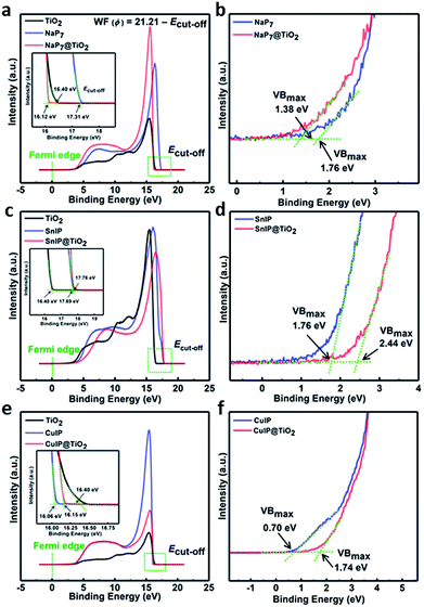
To gain insight into the charge transfer mechanisms in the materials and determine the band structure of the materials, work function spectra and valence band spectra were recorded using ultraviolet photoelectron spectroscopy (UPS). The work function was calculated using the expression WF (ϕ) = 21.21 − Ecut-off, where 21.21 eV is the energy of the incident He(I) line of a He discharge lamp, and Ecut-off is the cut-off energy of secondary electrons. The point of intersection after extrapolation of the linear regions of the graphs results in the cut-off energy values. From the graph, the cut-off energy and value of work function for TiO2, NaP7, NaP7@TiO2, (CuI)3P12, (CuI)3P12@TiO2, SnIP and SnIP@TiO2 are listed in Table 2 (Fig. 10 and insets). It should be noted that unexpectedly, we observe that the WF of the NaP7@TiO2 and SnIP@TiO2 hybrids falls above and below that of the pristine materials, respectively. This may be due to small amounts of metal-ion surface doping in the hybrids, where Na+ decreases the charge density on TiO2 and Sn2+ increases the charge density on TiO2; on the other hand, Cu+ is a closed-shell d-block element with a similar charge distribution to Ti4+, which may explain why this effect does not seem to be observed as strongly in this case. Furthermore, based on the P 2p region in NaP7, a higher degree of oxidation seems to occur in the pristine material compared to its hybrid here, changing the charge distribution on the phosphide backbone, and shifting the WF. The position of valence band maxima (VBmax) obtained from UPS valence band spectra of NaP7, NaP7@TiO2, (CuI)3P12, (CuI)3P12@TiO2, SnIP and SnIP@TiO2 is also shown in Table 2 (Fig. 10, inset). Furthermore, the valence band position of bare TiO2 nanotubes determined from XPS valence band spectra was found to be 3.15 eV below the Fermi level (Fig. S9†).
| Sample | E cut-off [eV] | WF [eV] | VBmax |
|---|---|---|---|
| TiO2 | 16.40 | 4.81 | 3.15 |
| NaP7 | 17.31 | 3.90 | 1.76 |
| NaP7@TiO2 | 16.12 | 5.09 | 1.38 |
| SnIP | 17.69 | 3.52 | 1.76 |
| SnIP@TiO2 | 17.76 | 3.45 | 2.44 |
| (CuI)3P12 | 16.06 | 5.15 | 0.70 |
| (CuI)3P12@TiO2 | 16.15 | 5.06 | 1.74 |
On the basis of the obtained band structure and band gap, we have proposed a plausible mechanism of improved photocatalytic performance of polyphosphide@TiO2 materials (Fig. 10). In general, to achieve efficient water splitting the conduction band position of the semiconductor should be more negative than 0.00 V vs. NHE at pH-0 (reduction potential of protons, H+/H2) and overpotential, while the valence band position should be more positive than +1.23 V vs. NHE at pH-0 (oxidation potential of water, H2O/O2). So, the band gap of the materials should be wider than 1.23 eV. TiO2 has a wide band gap of approximately 3.2 eV with appropriate band positions (conduction band, ECB; −0.26 V and valence band, EVB; +2.94 V vs. NHE at pH 0) to drive the water splitting reaction; however, its large band gap means the photocatalytic response of TiO2 remains too low under visible irradiation. On the other hand, inorganic phosphides (NaP7, (CuI)3P12 and SnIP) absorb well in the UV-Vis region to generate electron–hole pairs due to their low band gap (1.28, 2.84 and 1.86 eV) (Fig. S6†). From the Mott–Schottky measurements, the flat band potential values for NaP7, (CuI)3P12 and SnIP were found to be −0.670, −0.721 and −0.730 V, respectively, vs. Ag/AgCl, which might be considered the position of the conduction band, ECB (Table 2). As the band position is usually expressed on the NHE scale in water splitting, the conduction band position of NaP7, (CuI)3P12 and SnIP was calculated to be −0.471, −0.522 and −0.531 V, respectively, vs. NHE at pH 0. By taking the band gap and conduction band position into account, the estimated valence band position for NaP7, (CuI)3P12 and SnIP was found to be +0.809, +2.318 and +1.309 V, respectively, vs. NHE at pH 0. These values indicate that the valence band positions of NaP7 and SnIP are not positive enough to afford water oxidation, while the valence band position of (CuI)3P12 was slightly more positive than the water oxidation potential and thus generates poorly oxidizing holes. This explains the observed negligibly small photocurrent for pristine NaP7 and SnIP, and the slightly improved photocurrent for (CuI)3P12. After hybrid material formation, the photocatalytic performance of NaP7@TiO2, (CuI)3P12@TiO2 and SnIP@TiO2 was improved (Fig. 9d). However, SnIP@TiO2 displayed a much greater rise in photocurrent compared to the other hybrid nanostructures. The improved photocurrent response can possibly be explained based on the Fermi level alignment between heterojunctions, charge carrier concentration, flat band potential and position of the valence band. This feature has been observed for fibrous red phosphorus@TiO2 and black phosphorus@TiO2 hybrids.47 A drastic improvement of the photocatalytic activity was also reported for SnIP@C3N4 heterostructures where an ideal contact between the two materials is realized by a self-assembly process.48 Additional experiments are planned to substantiate this assumption for the titular compounds. Mott–Schottky analysis shows a shift in the flat band potential from −0.471 and −0.522 V vs. NHE in pristine NaP7 and (CuI)3P12 to −0.581 and −0.493 V vs. NHE in NaP7@TiO2 and (CuI)3P12@TiO2 which implies a possible Fermi level alignment (flow of electrons from one semiconductor to another for equilibrating the Fermi level position), and the conduction band shifted slightly due to downward band bending in NaP7 and (CuI)3P12 and upward band bending in TiO2, respectively, (see Fig. S17 in the ESI†). Interestingly, the conduction band position (ECB) of SnIP (−0.531 V) was shifted drastically toward a more negative potential in SnIP@TiO2 (−1.731 V), which reveals more prominent band bending. The higher band bending and more negative conduction band position in SnIP@TiO2 lead to more efficient charge separation, which facilitated superior water splitting.
From the UPS VB spectra, the VBmax position of SnIP@TiO2 was found to be deeper than that of NaP7@TiO2 and (CuI)3P12@TiO2 which suggests the generation of more oxidative holes in the SnIP@TiO2 heterostructure to drive water splitting (Fig. 10). Additionally, the depletion width for SnIP@TiO2 was found to be 922.89 nm which demonstrates an effective inbuilt electrical field in the space charge region; this value was much higher than that of NaP7@TiO2 (118.95 nm) and (CuI)3P12@TiO2 (157.14 nm), and clearly supports better charge transfer in SnIP@TiO2 (Table 2). Furthermore, the recombination lifetime of photoexcited species plays an important role in photocatalysis and a long lifetime is expected for better photocatalytic performance. The longer recombination lifetime of SnIP@TiO2 (2.40 μs) in comparison to NaP7@TiO2 (1.90 μs) and (CuI)3P12@TiO2 (1.90 μs) signifies the availability of more electrons and holes to drive hydrogen evolution and water oxidation reactions (Table 2). The morphological and surface coverage might be responsible for the higher performance of the SnIP@TiO2 nanostructure. SnIP has a helical structure composed of an inner P helix 1∞[P−] chain and an outer helical 1∞[SnI+] helix winding together in long range ordering which generates a rod like structure. Due to long range ordering in 1D SnIP, better charge mobility can be achieved relative to short range NaP7 and (CuI)3P12 resulting in better charge transfer to TiO2. The occupancy of the nanotubes was also much higher in NaP7@TiO2 and (CuI)3P12@TiO2 than SnIP@TiO2, which might reduce the effective exposed surface area to light and electrolyte semiconductor interface contact leading to lower photocatalytic performance.
3. Conclusions
A gas-phase transport reaction was employed as an effective method to deposit complex binary and ternary polyphosphide compounds into TiO2 nanotube arrays. The underlying short-way transport reaction by mineralization is a viable approach for the synthesis of hybrid materials. Three different substances, binary sodium polyphosphides, ternary SnIP, and (CuI)3P12, were successfully reacted with electrochemically fabricated TiO2 nanotube membranes. The synthesized polyphosphides onto and into the TiO2 nanotubes were analyzed with several spectroscopic and diffraction methods such as XRD, EDS-analysis, XPS, Auger electron and Raman spectroscopy and STEM analysis. SEM, HR-TEM, Auger electron spectroscopy, and elemental mapping of intact and cross sections of nanohybrids substantiated the successful deposition of materials inside the tube with excellent occupancy (a filling grade of ∼50%).STEM followed by EDS analysis proved the presence of the binary NaPx phase as well as (CuI)3P12 along the full length of the TiO2 nanotubes. STEM-EDS experiments of the ternary phase SnIP showed a higher distribution of P than Sn and I along TiO2 nanotubes. Raman spectra recorded at the surface and along the razor-cut cross section of the nanotubes can verify the growth of NaPx phases continuously along the nanotubes (120 μm in length) and (CuI)3P12 up to 22 μm into the nanotubes (63 μm in length). The herein reported hybrid materials displayed enhanced photoelectrochemical water splitting performance under visible light compared to individual components due to the possible formation of a heterojunction facilitating better charge separation. Considering the unusual values of the WF of NaP7@TiO2 and SnIP@TiO2, further study of the interfaces may be warranted. Nevertheless, lower electronic bandgaps, negative conduction band positions of the composites, long recombination lifetime, better charge carrier mobility and deep valence band positions were responsible for improved visible light performance. This feature may lead to higher conversion efficiencies for optoelectronic applications such as in photodetectors, photovoltaics, photo-electrochemical catalysts and sensors. With a special focus on the mineralization concept, further heterostructures between 1D semiconductors and nanostructured materials are being prepared.
Authors contribution
E. Ü. and R. K. synthesized the polyphosphide hybrid materials and characterized them using Helium Microscopy, SEM, and STEM-EDS. P. Kumar performed XPS, UPS and photoelectrochemical studies and was involved in the interpretation of the obtained results. U. K. T. carried out the KPFM measurements. P. Kar was responsible for the electrochemical characterization. K. S. and T. N. supervised the research and edited the manuscript. All authors were involved in writing their respective parts.Conflicts of interest
There are no conflicts to declare.Abbreviations
| CuIP | (CuI)3P12 |
| SEM | Scanning electron microscopy |
| EDS | Energy dispersive X-ray spectroscopy |
| FIB | Focused ion beam |
| HR-TEM | High resolution transmission electron microscopy |
| XRD | X-ray diffraction |
| XPS | X-ray photoelectron spectroscopy |
| STEM | Scanning transmission electron microscopy |
| ITO | Indium-doped tin oxide |
| FTO | Fluorine-doped tin oxide |
| UV-Vis | Ultraviolet-visible spectroscopy |
| NHE | Normal hydrogen electrode |
Acknowledgements
This work has been performed as part of the international graduate school ATUMS (IRTG 2022) funded by the DFG and NSERC. The assistance in Helium ion microscopy (with Ga-FIB), AES, and STEM-EDS by Peng Li, Shihong Xu and Anqiang He from the nanoFab at the University of Alberta is gratefully acknowledged. We like to thank Anna Vogel for Raman spectroscopy of the samples. The authors would like to thank the Natural Sciences and Engineering Research Council of Canada (NSERC), the National Research Council Canada (NRC), Future Energy Systems (FES) and CMC Microsystems for direct and indirect (equipment use) financial support. Pawan Kumar is thankful to Future Energy systems for providing the postdoctoral fellowship. Dr Kazi Alam is kindly acknowledged for the DR UV-Vis measurement. The use of Prof. Thomas Thundat's scanning probe microscope for the KPFM measurements is gratefully acknowledged.References
- T. Hisatomi, J. Kubota and K. Domen, Chem. Soc. Rev., 2014, 43, 7520–7535 RSC.
- P. Kalisman, Y. Nakibli and L. Amirav, Nano Lett., 2016, 16, 1776–1781 CrossRef CAS PubMed.
- K. Iwashina and A. Kudo, J. Am. Chem. Soc., 2011, 133, 13272–13275 CrossRef CAS.
- M. Higashi, K. Domen and R. Abe, J. Am. Chem. Soc., 2012, 134, 6968–6971 CrossRef CAS PubMed.
- J. Schneider, M. Matsuoka, M. Takeuchi, J. Zhang, Y. Horiuchi, M. Anpo and D. W. Bahnemann, Chem. Rev., 2014, 114, 9919–9986 CrossRef CAS PubMed.
- Y. Ma, X. Wang, Y. Jia, X. Chen, H. Han and C. Li, Chem. Rev., 2014, 114, 9987–10043 CrossRef CAS.
- J. Tang, J. R. Durrant and D. R. Klug, J. Am. Chem. Soc., 2008, 130, 13885–13891 CrossRef CAS PubMed.
- S. J. A. Moniz, S. A. Shevlin, D. J. Martin, Z.-X. Guo and J. Tang, Energy Environ. Sci., 2015, 8, 731–759 RSC.
- K. Iwashina, A. Iwase, Y. H. Ng, R. Amal and A. Kudo, J. Am. Chem. Soc., 2015, 137, 604–607 CrossRef CAS PubMed.
- Z. Yu, F. Li and L. Sun, Energy Environ. Sci., 2015, 8, 760–775 RSC.
- Y.-C. Pu, G. Wang, K.-D. Chang, Y. Ling, Y.-K. Lin, B. C. Fitzmorris, C.-M. Liu, X. Lu, Y. Tong, J. Z. Zhang, Y.-J. Hsu and Y. Li, Nano Lett., 2013, 13, 3817–3823 CrossRef CAS PubMed.
- M. Ge, Q. Li, C. Cao, J. Huang, S. Li, S. Zhang, Z. Chen, K. Zhang, S. S. Al-Deyab and Y. Lai, Adv. Sci., 2017, 4, 1600152 CrossRef PubMed.
- R. Singh, R. Bapat, L. Qin, H. Feng and V. Polshettiwar, ACS Catal., 2016, 6, 2770–2784 CrossRef CAS.
- M. Bawohl and T. Nilges, Z. Anorg. Allg. Chem., 2015, 641, 304–310 CrossRef CAS.
- M. Bawohl, P. Schmidt and T. Nilges, Inorg. Chem., 2013, 52, 11895–11901 CrossRef CAS.
- M. P. Baumgartner, Dissertation (Dr. rer. nat.), Technische Universität München, 2017.
- D. Pfister, K. Schäfer, C. Ott, B. Gerke, R. Poettgen, O. Janka, M. Baumgartner, A. Efimova, A. Hohmann, P. Schmidt, S. Venkatachalam, L. van Wuellen, U. Schürmann, L. Kienle, V. Duppel, E. Parzinger, B. Miller, J. Becker, A. Holleitner, R. Weihrich and T. Nilges, Adv. Mater., 2016, 28, 9783–9791 CrossRef CAS PubMed.
- C. Grotz, M. Köpf, M. Baumgartner, L. A. Jantke, G. Raudaschl-Sieber, T. F. Fässler and T. Nilges, Z. Anorg. Allg. Chem., 2015, 641, 1395–1399 CrossRef CAS.
- M. Schöneich, A. Hohmann, P. Schmidt, F. Pielnhofer, F. Bachhuber, R. Weihrich, O. Osters, M. Köpf and T. Nilges, Z. Kristallogr. - Cryst. Mater., 2017, 232, 91–105 Search PubMed.
- S. Lange, M. Bawohl, R. Weihrich and T. Nilges, Angew. Chem., Int. Ed., 2008, 47, 5654–5657 CrossRef CAS PubMed.
- A. Utrap, N. Y. Xiang and T. Nilges, J. Cryst. Growth, 2017, 475, 341–345 CrossRef CAS.
- C. Grotz, K. Schäfer, M. Baumgartner, R. Weihrich and T. Nilges, Inorg. Chem., 2015, 54, 10794–10800 CrossRef CAS PubMed.
- A. Pfitzner and E. Freudenthaler, Angew. Chem., Int. Ed., 1995, 34, 1647–1649 CrossRef CAS.
- D. Regonini, C. R. Bowen, A. Jaroenworaluck and R. Stevens, Mater. Sci. Eng., R, 2013, 74, 377–406 CrossRef.
- R. Hahn, J. Macak and P. Schmuki, Electrochem. Commun., 2007, 9, 947–952 CrossRef CAS.
- P. Kar, Y. Zhang, S. Farsinezhad, A. Mohammadpour, B. D. Wiltshire, H. Sharma and K. Shankar, Chem. Commun., 2015, 51, 7816–7819 RSC.
- B. M. Rao and S. C. Roy, J. Phys. Chem. C, 2013, 118, 1198–1205 CrossRef.
- V. Galstyan, A. Vomiero, E. Comini, G. Faglia and G. Sberveglieri, RSC Adv., 2011, 1, 1038–1044 RSC.
- S. Farsinezhad, A. Mohammadpour, A. N. Dalrymple, J. Geisinger, P. Kar, M. J. Brett and K. Shankar, J. Nanosci. Nanotechnol., 2013, 13, 2885–2891 CrossRef CAS PubMed.
- S. Farsinezhad, A. N. Dalrymple and K. Shankar, Phys. Status Solidi A, 2014, 211, 1113–1121 CrossRef CAS.
- X. Chen, M. Schriver, T. Suen and S. S. Mao, Thin Solid Films, 2007, 515, 8511–8514 CrossRef CAS.
- A. Mohammadpour and K. Shankar, J. Mater. Chem., 2010, 20, 8474–8477 RSC.
- D. Routkevitch, T. Haslett, L. Ryan, T. Bigioni, C. Douketis and M. Moskovits, Chem. Phys., 1996, 210, 343–352 CrossRef CAS.
- Y. Peng, D.-H. Qin, R.-J. Zhou and H.-L. Li, Mater. Sci. Eng., B, 2000, 77, 246–249 CrossRef.
- D. Xu, X. Shi, G. Guo, L. Gui and Y. Tang, J. Phys. Chem. B, 2000, 104, 5061–5063 CrossRef CAS.
- M. Lu, M.-K. Li, L.-B. Kong, X.-Y. Guo and H.-L. Li, Composites, Part B, 2004, 35, 179–184 CrossRef.
- A. Mohammadpour, P. Kar, B. D. Wiltshire, A. M. Askar and K. Shankar, Curr. Nanosci., 2015, 11, 593–614 CrossRef CAS.
- N. S. Lewis, Science, 2007, 315, 798–801 CrossRef CAS PubMed.
- X. Zhang, F. Han, B. Shi, S. Farsinezhad, G. P. Dechaine and K. Shankar, Angew. Chem., Int. Ed., 2012, 51, 12732–12735 CrossRef CAS PubMed.
- D. Zhou, Z. Chen, Q. Yang, C. Shen, G. Tang, S. Zhao, J. Zhang, D. Chen, Q. Wei and X. Dong, ChemCatChem, 2016, 8, 3064–3073 CrossRef CAS.
- X. Fu, Z. Ji, C. Li and Z. Zhou, J. Alloys Compd., 2016, 688, 1013–1018 CrossRef CAS.
- Z. Lou, F. Li, J. Deng, L. Wang and T. Zhang, ACS Appl. Mater. Interfaces, 2013, 5, 12310–12316 CrossRef CAS PubMed.
- P. Qin, M. Paulose, M. I. Dar, T. Moehl, N. Arora, P. Gao, O. K. Varghese, M. Grätzel and M. K. Nazeeruddin, Small, 2015, 11, 5533–5539 CrossRef CAS PubMed.
- U. K. Thakur, R. Kisslinger and K. Shankar, Nanomaterials, 2017, 7, 95 CrossRef PubMed.
- Z. Xiong, H. Wang, N. Xu, H. Li, B. Fang, Y. Zhao, J. Zhang and C. Zheng, Int. J. Hydrogen Energy, 2015, 40, 10049–10062 CrossRef CAS.
- J. Low, B. Cheng and J. Yu, Appl. Surf. Sci., 2017, 392, 658–686 CrossRef CAS.
- E. Üzer, P. Kumar, R. Kisslinger, P. Kar, U. K. Thakur, S. Zeng, K. Shankar and T. Nilges, ACS Appl. Nano Mater., 2019 DOI:10.1021/acsanm.9b00221.
- C. Ott, F. Reiter, M. Baumgartner, M. Pielmeier, A. Vogel, P. Walke, S. Burger, M. Ehrenreich, G. Kieslich, D. Daisenberger, J. Armstrong, U. K. Thakur, P. Kumar, S. Chen, D. Donadio, L. S. Walter, R. T. Weitz, K. Shankar and T. Nilges, Adv. Funct. Mater., 2019, 29, 1900233 CrossRef.
Footnotes |
| † Electronic supplementary information (ESI) available. See DOI: 10.1039/c9na00084d |
| ‡ Contributed equally. |
| This journal is © The Royal Society of Chemistry 2019 |

