
 Open Access Article
 This Open Access Article is licensed under a Creative Commons Attribution-Non Commercial 3.0 Unported Licence
Nanocrystalline graphene at high temperatures: insight into nanoscale processes†
C. N. Shyam
Kumar
ab,
Manuel
Konrad
a,
Venkata Sai Kiran
Chakravadhanula‡
 c,
Simone
Dehm
a,
Di
Wang
ad,
Wolfgang
Wenzel
a,
Ralph
Krupke
ab and
Christian
Kübel
*abcd
c,
Simone
Dehm
a,
Di
Wang
ad,
Wolfgang
Wenzel
a,
Ralph
Krupke
ab and
Christian
Kübel
*abcd
aInstitute of Nanotechnology, Karlsruhe Institute of Technology, 76021 Karlsruhe, Germany. E-mail: christian.kuebel@kit.edu
bDepartment of Materials and Earth Sciences, Technical University Darmstadt, 64287 Darmstadt, Germany
cHelmholtz Institute Ulm, Karlsruhe Institute of Technology, 76021 Karlsruhe, Germany
dKarlsruhe Nano Micro Facility, Karlsruhe Institute of Technology, 76021 Karlsruhe, Germany
First published on 23rd April 2019
Abstract
During high temperature pyrolysis of polymer thin films, nanocrystalline graphene with a high defect density, active edges and various nanostructures is formed. The catalyst-free synthesis is based on the temperature assisted transformation of a polymer precursor. The processing conditions have a strong influence on the final thin film properties. However, the precise elemental processes that govern the polymer pyrolysis at high temperatures are unknown. By means of time resolved in situ transmission electron microscopy investigations we reveal that the reactivity of defects and unsaturated edges plays an integral role in the structural dynamics. Both mobile and stationary structures with varying size, shape and dynamics have been observed. During high temperature experiments, small graphene fragments (nanoflakes) are highly unstable and tend to lose atoms or small groups of atoms, while adjacent larger domains grow by addition of atoms, indicating an Ostwald-like ripening in these 2D materials, besides the mechanism of lateral merging of nanoflakes with edges. These processes are also observed in low-dose experiments with negligible electron beam influence. Based on energy barrier calculations, we propose several inherent temperature-driven mechanisms of atom rearrangement, partially involving catalyzing unsaturated sites. Our results show that the fundamentally different high temperature behavior and stability of nanocrystalline graphene in contrast to pristine graphene is caused by its reactive nature. The detailed analysis of the observed dynamics provides a pioneering overview of the relevant processes during ncg heating.
Introduction
Even after more than a decade since its first successful exfoliation, graphene continues to be an interesting material for different technological applications because of its unique properties.1,2 Different fabrication techniques have been developed to produce graphene with varying size, shape and properties.3 However, extended application of graphene is still hindered by the challenges in transferring defect and contamination free graphene to various substrates for reliable device fabrication. Graphitization of polymer thin films to synthesize graphenoid (graphene like) materials has emerged as an easy to fabricate alternative for graphene for various applications.4,5 The method provides the flexibility of growing on different substrates with defined thickness and also for patterning to achieve different shapes.5,6 Recently, thin graphitized films with comparable electrical and optical properties to graphene, were fabricated by pyrolysis of polymer thin films.6,7 The catalyst-free growth results in a material with domain sizes of a few nanometers, which has been termed nanocrystalline graphene (ncg). The ease of fabrication, control over size, shape and thickness, and the possibility to tailor the properties by varying the polymer precursor and the graphitization conditions has made this material a potential alternative for polycrystalline graphene in areas such as electronics,7,8 photonics,4,6 strain sensing,6 and transparent conducting electrodes.9,10Graphitization of polymers by pyrolysis at high temperatures to produce graphite or bulk glassy carbons is a well-established process.11–13 Various experimental methods like X-ray diffraction,14 Raman spectroscopy15 and transmission electron microscopy (TEM)16 have been used to study and understand the graphitization process in detail and different models have been proposed.16–18 Graphitization at small length scales has gained importance because of the developments in carbon micro electro mechanical systems and nano electro mechanical systems (C-MEMS and NEMS).19 A proper understanding of the graphitization process is important to tailor the structure and properties for different applications. Low-voltage transmission electron microscopy is a versatile tool for sub-angstrom level characterization of graphene and other related materials without inducing significant damage to the material.20–23 Improvements in in situ low-voltage HRTEM capabilities enabled a detailed examination of transient stages in various dynamic processes at different spatial and temporal scales, which are otherwise difficult to observe and analyze in these carbon nanostructures.24–26
In previous work, we studied the graphitization and domain growth of free-standing nanocrystalline graphene thin films prepared by vacuum annealing of a photoresist inside a TEM and followed the process by various in situ TEM techniques. The in situ studies showed that the graphitization process is highly dynamic with a number of intermediate reactions leading to the formation of different carbon nanostructures. The catalyst-free transformation of amorphous carbon on the top of graphitic substrates results in the formation of carbon nanostructures with different size, shape and mobility.27In situ high temperature studies on ncg provide the possibility to understand the stability, dynamics and reactions of these nanostructures and their interaction with the graphitic substrate. Analyzing these interactions can help to understand the fundamental mechanisms that control graphene growth at high temperatures and thus can be used to tailor its properties.
Even though a lot of research has been performed in the area of high temperature behavior of graphene using in situ TEM techniques, most of the studies have been carried out on single layer graphene with a focus on the stability and dynamics of individual defects or small groups of defects.20,28–30In situ TEM studies of the behavior of small carbon nanostructures on top of a graphitic substrate were mostly carried out at room temperature and the transformations were driven by electron beam induced effects.31–34 The ncg films with a high density of defects, active edges and carbon nanostructures employed in this study provide a completely different system to study the high temperature dynamics and reactions of carbon nanostructures.
Here we conduct a series of in situ high temperature experiments. From time resolved HRTEM data, we identify several characteristic processes and assess their roles in the polymer pyrolysis supported by molecular dynamics simulations to complete the nanoscopic picture. Furthermore, we investigate the influence of the electron beam by experiments with drastically reduced radiation dose. They reveal that atom rearrangement and transfer processes are inherent temperature-driven processes. Theoretical energy barrier calculations support this observation and various atom rearrangement pathways are proposed. Especially, we discuss the facilitating/catalyzing effect of reactive defect sites and edges on atom transfer processes. Overall, the analysis of the numerous observed processes during the heating experiments illustrates the different high temperature behavior of ncg compared to coarse grained polycrystalline graphene. Our study gives a detailed insight into the nanoscale processes during pyrolysis and forms the basis for future work towards application in device manufacturing.
Experimental
Preparation of freestanding nanocrystalline graphene
The commercially available photoresist, microposit S1805, was used as carbon source for the preparation of nanocrystalline graphene. The photoresist was diluted with propylene glycol monomethyl ether acetate (PGMEA) 1![[thin space (1/6-em)]](https://www.rsc.org/images/entities/char_2009.gif) :12 to control the viscosity and film thickness. The resist was spin coated onto a MEMS based heating chip (Protochips Inc.) at 8000 rpm for 30 seconds and then baked at 160 °C for 3 minutes resulting in a thin film completely covering the heating chip. The chip was transferred to a heating holder (Aduro 500 by Protochips Inc.). The initial heating was carried out inside a pumping station (Gatan Inc.) at 10−7 mbar at a temperature of 600 °C for 5 hours (heating rate 10 °C per minute) to prevent contamination of the TEM by the large amount of gas released during the initial stages of graphitization.
:12 to control the viscosity and film thickness. The resist was spin coated onto a MEMS based heating chip (Protochips Inc.) at 8000 rpm for 30 seconds and then baked at 160 °C for 3 minutes resulting in a thin film completely covering the heating chip. The chip was transferred to a heating holder (Aduro 500 by Protochips Inc.). The initial heating was carried out inside a pumping station (Gatan Inc.) at 10−7 mbar at a temperature of 600 °C for 5 hours (heating rate 10 °C per minute) to prevent contamination of the TEM by the large amount of gas released during the initial stages of graphitization.
In situ TEM investigations
An aberration corrected (image) Titan 80-300 TEM (FEI Company) operated at 80 kV equipped with a US1000 slowscan CCD (Gatan Inc.) camera was used for imaging. The in situ heating experiments were carried out at a heating rate of 10 °C per minute. The pre-carbonized samples were heated inside the TEM with the electron beam turned off until the desired temperature was reached. The same heating rate of 10 °C per minute was used in all experiments. The beam was blanked in between image acquisition to minimize beam-induced effects. Images were acquired with an interval of 5 s with a 1 s exposure time. The dose for each single high-resolution TEM image varied between 2.0 × 10⁷ e nm−2 and 4.1 × 10⁸ e nm−2 depending on the magnification. We have carried out 16 different heating experiments at various temperatures using 4 different samples. Out of more than hundred different events observed during heating, 30 independent events were analyzed in detail to understand the main structural changes occurring during heating.Computational methods
The molecular dynamics simulations where conducted with the LAMMPS package35 using the AIREBO force field for hydrocarbons.36 Nudged elastic band (NEB) calculations37 and steered molecular dynamics (SMD) simulations were carried out with the ASE package38 in conjunction with the semi-empirical solver MOPAC (MOPAC2016, Version: 18.117L),39 using the PM7 functional.40 For the NEB calculations spring constants of 0.01 eV Å−1 and a convergence criterion of fmax = 0.1 eV Å−1 were used, the transition states were determined with a climbing image. The visualizations in this work were created with the OVITO software.41Results and discussions
Migration and merging of graphene flakes
Fig. 1 shows the migration and merging of a small graphitic flake at 1200 °C. The flake was not visible during the first 118 frames (590 s) of observation (ESI Video S1†) and suddenly appeared in the next frame (Fig. 1b). The flake is stable at this position for the next 20 frames (100 s), ‘jumps’ to a nearby position and comes back to the original position in the next two frames (Fig. 1c/d). The flake is pinned to the initial position for the next 84 frames (420 seconds) and finally ‘jumps’ and attaches to an edge, which is around 10 nm away, and rapidly merges with the edge thus extending the grain (Fig. 1e). The merging of the flakes happen within two frames (Fig. 1e and f) and is followed by a fast rearrangement of the newly formed edge of the carbon grain. This observed migration is different and slower than the previously reported high mobility of carbon nanostructures and graphene nanoflakes on top of a graphitic substrate with weak interactions between nanostructures and substrate.31,42,43 Previous experimental observations have shown a super fluidic behavior of graphene nanoflakes (GNF) even at temperatures as low as 5 K.44 Similarly, theoretical calculations show a high diffusion coefficient of (6.7 ± 0.6) × 10−6 cm2 s−1 for GNF on top of defect-free graphene substrates at 300 K.43 This is consistent with our molecular dynamics studies (MD) at 1500 K, which also show fast diffusion of GNF on top of graphene (ESI Video S2†). Considering this high mobility of GNF on top of graphene, it would not be possible to image this migration at high temperatures with our current exposure time of 1 s. However, in case of nanocrystalline graphene, the graphene substrate is highly defective and the defects limit diffusion by locally pinning GNFs. MD simulations of GNFs on substrates with point defects show bond formation of the reactive flake edge with unsaturated substrate atoms (Fig. 1f and ESI Video S3†). It is known that the strain fields near defects in the graphene lattice can even induce vertical displacements of carbon atoms close to the defect.45 Also, the nanoflake edges are highly reactive and constantly rearranging at high temperature (ESI Video S1†) which can facilitate bond formation and therefore pinning of the GNF. Since the defect density is high, there can be simultaneous bond formation at more than one site further reducing the mobility of the flake. This means that migration on highly defective nanocrystalline graphene is dominated by a hopping between defects, which depends on the nature and density of the defects. Out of the different observed events in our experiments, both the migration distance and the frequency of events vary significantly, depending on the size of the flake and presumably the defect density of the substrate.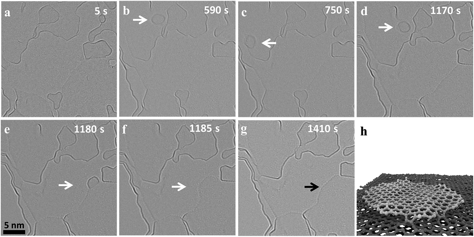 | ||
| Fig. 1 (a–g) Migration and merging of a nano-flake during heating at 1200 °C. The time stamp corresponding to the snap shot of the observed dynamics is shown as label in each micrograph. The initial merging is fast, occurring between frame (d) and (e). (h) shows a snapshot of a flake (diameter of approx. 3 nm, hydrogen-free edge) pinned to defects in the substrate in a MD simulation at 1500 K. | ||
Merging of flakes is initiated by bond formation between the active edges when they get close to each other. The MD simulations show this initial bond formation upon contact between the edge atoms of two similar sized flakes heated on the top of a graphitic substrate followed by formation of further bonds (ESI Video S4†). The frequency of merging events depends on the mobility of the nanoflakes and the availability of suitable edges nearby. As the structure of ncg is a complex stack of graphitic domains with a lot of free edges, it is difficult to precisely determine the layer on which a flake is moving based on the TEM images. The edges that are visible near the flake might be above or below the GNF and thus be out of the reach for the flake. The images show that, during migration, the nanoflakes exhibit strong vibrations and rotations, which is in agreement with nanoflakes being known to show strong structural fluctuations at high temperatures. Previous ab initio calculations revealed strong out-of-plane vibrations for the edges of an isolated nanoflake at high temperatures.46 Our MD simulations also show strong vibrations for the substrate and the nanoflake at high temperature (ESI Video S2†). These fast changes compared to the exposure time sometimes result in fuzzy edge structures in the experimental images. Nanostructures with stable size and edge contrast were also observed during heating (ESI Fig. 1†). The size of these nanostructures is in agreement with fullerene-like structures, which might have formed during the initial stages of graphitization. These close caged structures also migrate and are pinned by defects, but merging was not observed for these kinds of structures. Furthermore, it has been shown in a number of studies that few layer graphene can contain back-folded edges or bilayers,47,48 which are presumably also present in the nanocrystalline graphene investigated here. These structures are known to be more stable and less reactive and we suggest that the shape and size stability can be attributed to closed cage and folded structures.
Apart from edge fluctuations of the nanoflakes, the large flake edges also seem to be highly dynamic and constantly rearranging. Moiré patterns are observed intermittently indicating distinct commensurate arrangements between the layers leading to some superstructures as observed previously in bilayer graphene.49 The fast dynamics and the high reactivity indicates that these types of edges are not folded edges, but unsaturated ones with highly reactive dangling bonds. It should also be noted that the additional mass from the merging flake leads to a big step in the edge of the graphene crystallite, which is quickly distributed to the side, reducing the overall edge curvature until a new dynamic equilibrium is reached with a more or less flat edge (Fig. 1g). These observations show the highly dynamic and reactive nature of edges in graphene at high temperatures, which are critical for the high temperature dynamics of nanocrystalline graphene.
Our experiments also reveal cases where a flake merges with the step edge underneath, which results in a vertical mass transfer. Fig. 2 shows such a merging event of a small flake sitting on top of an edge and merging completely with the graphene layer underneath (ESI Video S1†). Unlike the rapid movement and merging observed for the lateral merging in Fig. 1, in this case the merging is slow and progressive. The flake exhibits uniform Fresnel contrast at the edge until Fig. 2c. Afterwards, the edge of the upper flake attaches to the step edge below (Fig. 2d). Subsequently, the edge of the upper flake slowly disappears as the flake is completely merging with the edge below. This means that the rearrangement and bonding mechanism is different in this type of merging. In order to move vertically at a step edge, the reactive edges of the flake and the step underneath must overlap and form a covalent bond, which could be observed in a MD simulation of the process (Fig. 2r). In order for the flake to fully merge with the edge underneath, the initial bonding has to shift leading to a transfer of the atom along the edge and a new bond has to be formed with another atom in the flake. This vertical merging requires a coordinated rearrangement at larger scales in contrast to the lateral rearrangements in the previous case. In the experiment, this slows down the vertical rearrangement to a time scale of several minutes, in contrast to the fast lateral merging shown in Fig. 1.
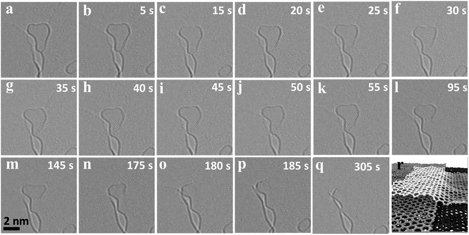 | ||
| Fig. 2 (a–q) Slow merging of a nanoflake with an edge in the layer underneath during heating at 1200 °C, the time interval is shown as label in each micrograph. (r) shows a MD simulation of pinning of a flake (dimensions of approx. 5.5 × 5 nm2, hydrogen-free edges) to the step edge below at 1500 K. | ||
Dynamics and size evolution of graphene flakes
In addition to the above described size increase due to merging of graphene flakes, we observed both a gradual mass loss and a gradual mass increase of nanoflakes in close proximity to each other. Fig. 3 shows an image series of such a shrinkage/growth process recorded at 1200 °C in 5 s intervals (ESI Video S5†). A gradual size reduction is observed for the small flake (indicated by white arrows) before it attaches and merges with an edge (b–g). During the same time, a big flake (indicated by black arrow) close to the shrinking flake is growing (h–m). This is one example illustrating that small flakes tend to lose atoms while the large ones grow under the same illumination and temperature conditions. A similar shrinking of a flake during migration can be observed in the ESI Fig. 2 and Video S6† where a flake moves along an edge on which the flake is sitting and loses atoms. At the same time, we can observe a growth in an adjacent large flake sitting on the same edge.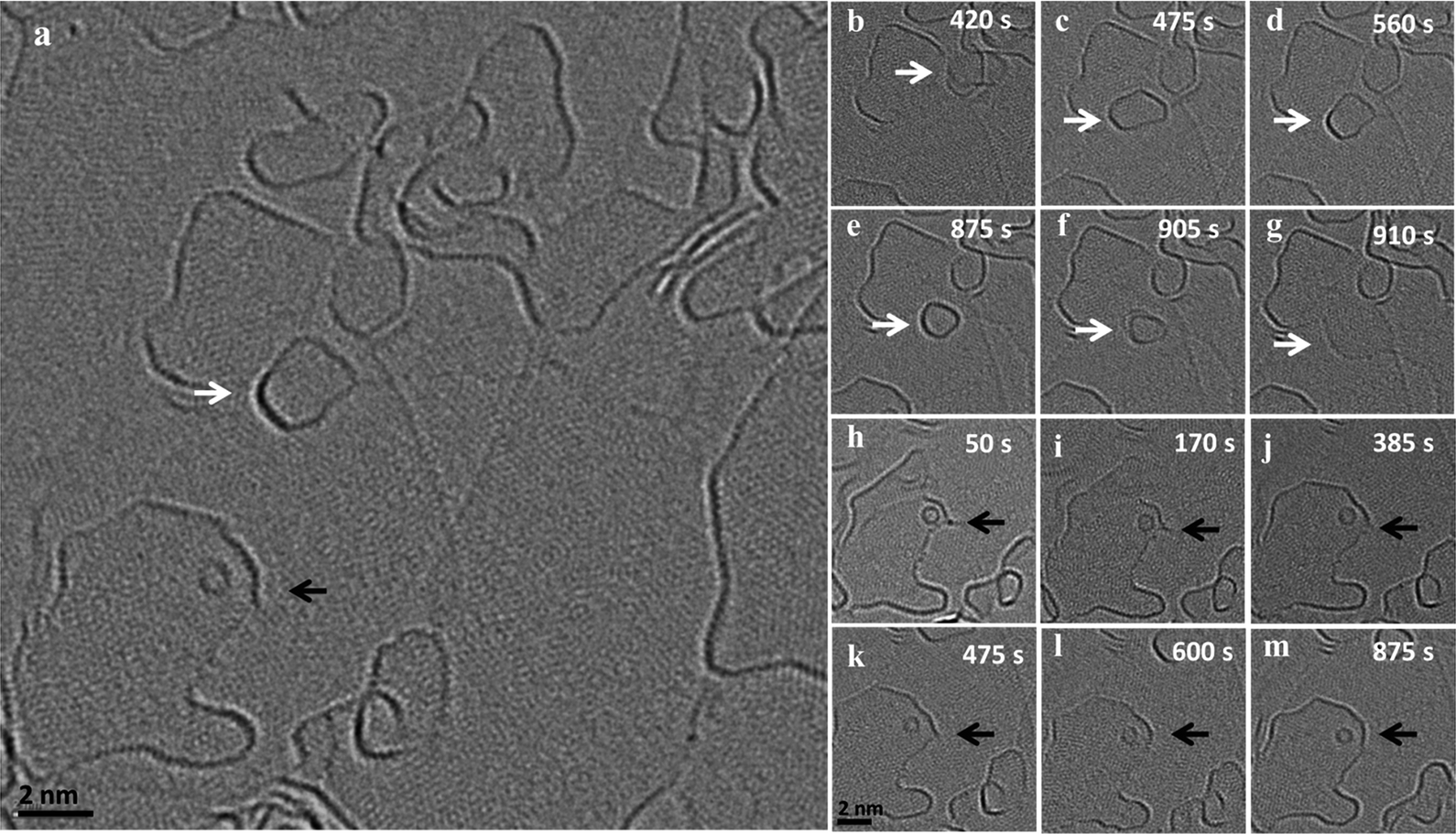 | ||
| Fig. 3 (a) HRTEM image of an area in which shrinkage of a migrating flake (indicated by the white arrow) and growth of a larger flake (indicated by black arrow) has been observed simultaneously. (b–g) shows the mass loss during migration of the flake and (h–m) the growth of the large flake by extending the edge. | ||
Fig. 4(a–f) shows the dynamics of a nanostructure pinned at an edge, which gradually disappears over a time interval of 14 minutes (ESI Video S7†). The nanostructure is not migrating or merging with the edge, but is rather pinned to a region and gradually shrinks in size and finally disappears. In the same frames, one can observe an active region in the adjacent edge, which is no longer continuous and seems to open up by the addition of atoms. Also, in this case the structure seems to sit on an edge which is connected to the large flake where the addition of atoms is happening (Fig. 4g). All of these examples suggest a mass transfer by individual atoms or small groups of atoms detaching from an unstable small nanostructure and attaching to a nearby stable large flake. This phenomenon looks similar to an Ostwald-like ripening, where small particles shrink and larger particles grow driven by the higher thermodynamic stability of the larger particles.
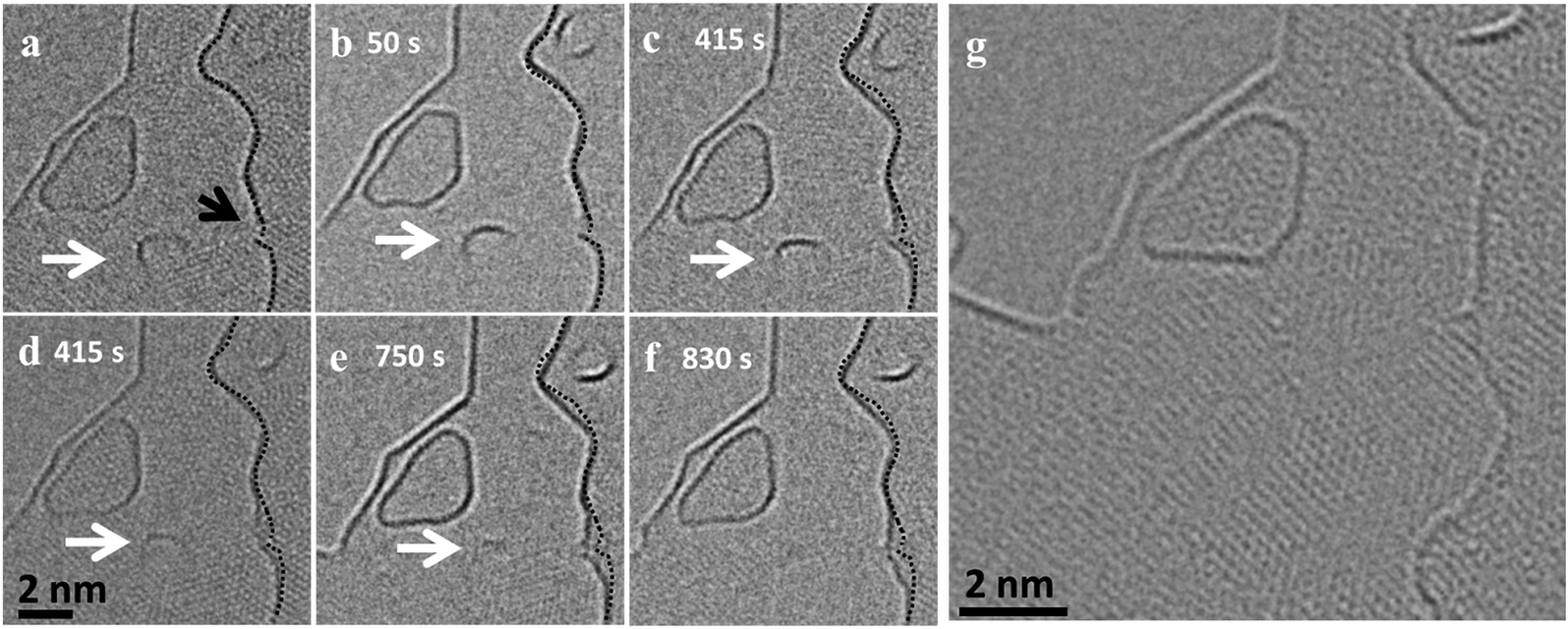 | ||
| Fig. 4 (a–f) HRTEM image of a slowly shrinking pinned nanostructure (marked by white arrow) at 900 °C and of an active region (marked by black arrow) in the adjacent layer where atoms are attaching, leading to a growth at the edge. The initial edge profile is overlaid on the following time steps to visualize the growth of the flake. (g) HRTEM image taken after the series acquisition, which shows the presence of a connecting edge between the shrinking nanoflake and the growing large flake. | ||
It is worth noting that the size reduction is observed in structures that are pinned to edges and defects (the structure in Fig. 1 also shows a reduction in size before it merges). As observed in the vertical merging, during pinning, there can be an atom transfer from the flake to edges and defects. We assume two different types of transfer happening: (1) transfer of atoms to underlying defects in the substrate accompanied by healing the defects and (2) transfer of atoms to an active edge below or nearby, where the atom can either migrate along the edge by edge diffusion to another connected flake or can be attached to the same edge extending the edge. This means that the highly active edges can act as a diffusion pathway for the atoms detaching from the flakes. Similarly, an extended defect structure like a line defect or a grain boundary may also act as a possible reactive site for atom transfer and further diffusion.
The effect of the defect density and the availability of active free edges on the behavior of the carbon nanostructures can be observed in ESI Fig. 3 and Video S8†. Here, two similar sized GNF behave differently when observed at the same conditions. While the isolated flake, which is far from any edges, is stable with negligible mass loss, the flake which is close to an edge loses atoms quickly and migrates out of the field of view. The flake near the edge will have the combined effect of the electron beam and nearby reactive sites which increase the removal rate, while the isolated flake is only affected by the beam. It is also worth noting that when two similar sized flakes get close together, in our observations, they always merge and we did not observe a continuous mass transfer in that case (ESI Fig. 4†).
For the analysis of these experiments, it is important to consider the influence of the electron beam on the processes. The high-energy electron beam is known to induce defects and structural changes in graphene and carbon nanostructures.20,22,50 There are a number of studies on purely beam induced transformations of carbon nanostructures on top of graphitic substrates at 80 kV.33,34,51 This means that the beam can have considerable effects on the dynamics of carbon nanostructures. The threshold for knock-on damage in graphene is just above 80 kV, therefore it is typically considered ‘safe’ to image graphene at 80 kV.25 However, the threshold for knock-on damage at edges and defects in graphene is considerably lower (around 50 kV26) resulting in some sputtering of edge atoms at 80 kV, which will contribute to the observed size reduction of graphene flakes. Moreover, ionization due to inelastic scattering can result in a transition of an electron in a bonding state to an antibonding state, which can lower the activation energy for bond rearrangement or breakage.52 Furthermore, electron beam sputtering can also act as a source to add new atoms or remove atoms. A high amount of ad-atoms have been observed previously during in situ heating of graphene in the TEM.29 These ad-atoms are highly mobile on top of the graphitic substrate and can attach and heal vacancies and nanopores at high temperatures.29 Besides sputtering, residual hydrocarbon impurities in the TEM column can also be a source for ad-atoms.25,29,53 The hydrocarbon impurities in the TEM column can be cracked and act as a carbon source, graphitizing on a graphitic substrate with and without the support of a catalyst.25,53 Experimental evidence in our investigations shows that the sample surface contains a large amount of highly active ad-atoms. This can be seen form the rapid filling of a hole during the initial period in Video S1,† where a hole of ∼2 nm diameter was completely filled in less than a minute. Another beam induced effect that can contribute to the reactions is the activation of oxygen, hydrogen and metallic impurities in the column by the electron beam. This can result in etching of graphene edges. Strong effects of catalytic etching and the edge structure on the addition and removal of carbon atoms have been explained well, both experimentally and theoretically, in previous studies of CVD grown graphene.54 In that study, increasing the hydrogen flow resulted in a reduction in flake size due to etching of the edge by atomic hydrogen formed because of the catalytic dissociation by platinum. The study also shows the effect of the edge structure and curvature on the etch rate.54 The electron beam is known to trigger similar dissociation of oxygen, hydrogen and water present inside the TEM column52 and can lead to an etching of the graphene edges. The edge structure, local curvature of the edges54 and the higher energy per atom55 results in higher probability to lose atoms for a small nanoflake compared to larger flakes. Our steered molecular dynamics (SMD) simulations (ESI Fig. 5†) also show the effect of local curvature on the atom displacement from an edge. This means that the electron beam can have a prominent effect on the observed dynamics and it is important to separate the effects due to temperature and due to the electron beam for the observed processes. Therefore, we performed heating experiments with the electron beam off for very extended times to eliminate/reduce the effect of the beam. In addition, we looked at electron beam damage at room temperature to further judge its effect (ESI Fig. 6†).
‘In situ’ heating with the electron beam off
To estimate the effects of the electron beam during the high temperature dynamics studies, we investigated the sample without electron beam illumination, just taking an image of the same area before and after heating for an extended period. Fig. 5 shows three such sets of images before and after heating with the electron beam off. Comparing Fig. 5a and b, we clearly observe migration of domains (indicated by a blue arrow) without the presence of the electron beam. This is similar during heating at 1200 °C for 20 minutes, where a nanoflake (indicated by a blue arrow) present in image c vanishes from the field of view during heating. This flake might have merged with the edge beneath it or has migrated to some other location. The flakes marked by green arrows are examples for merging without the presence of the electron beam. Flakes marked by red arrows in Fig. 5 exhibit a change in shape and reduction in size and the ones marked by white arrows show an increase in size. This shows that shrinking and growth of domains can also happen without the beam. The observed reduction in size is caused by detachment of atoms or groups of atoms, while an increase in size can be caused by the addition of atoms or by merging with a mobile flake. It is difficult to identify the active regions in a growing flake with this very large acquisition interval and with the dynamic nature of the edges, but these beam off heating results clearly show that the basic processes observed during heating with continuous imaging also occur without the electron beam, thus confirming that they are inherent temperature driven processes.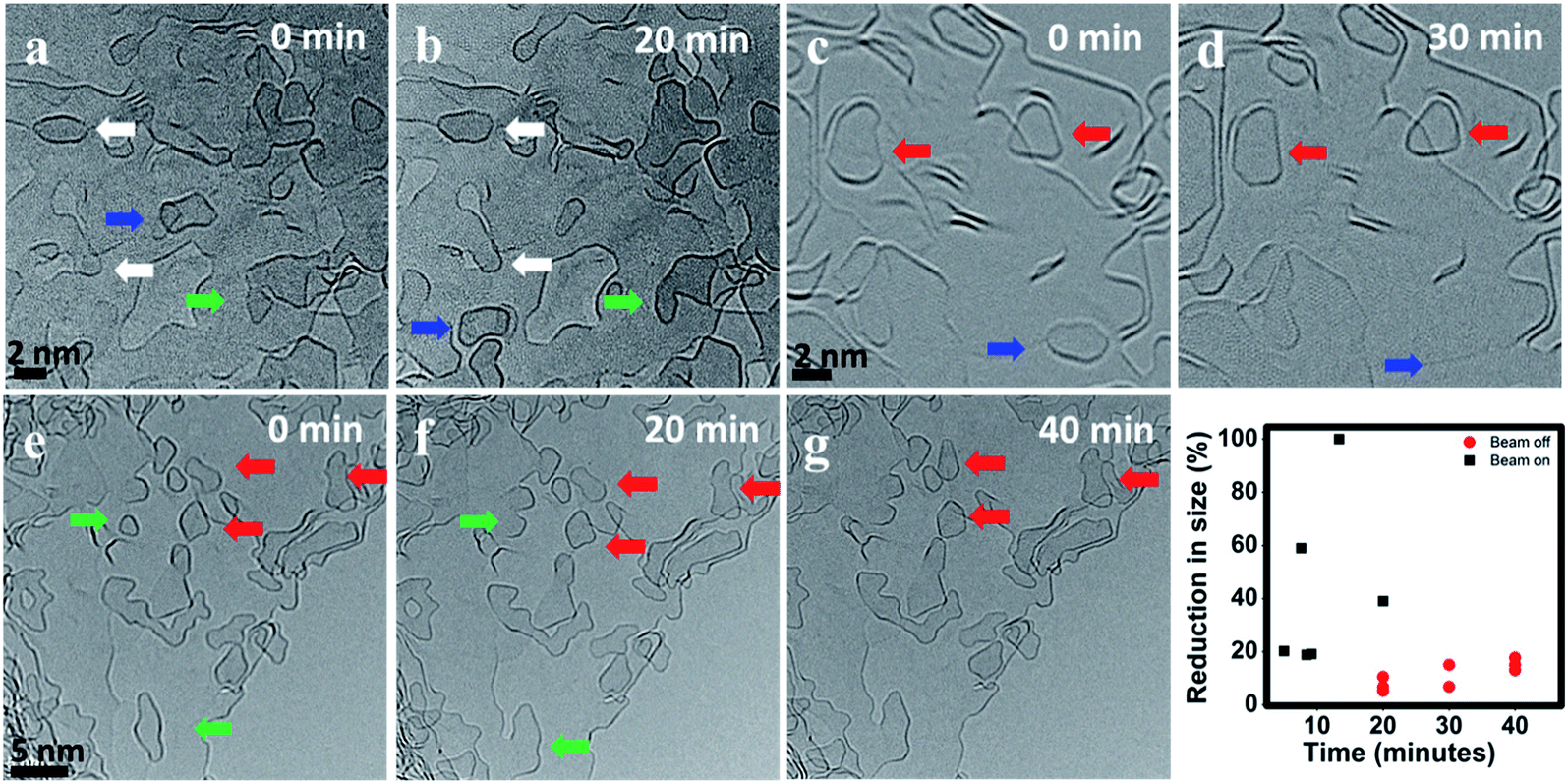 | ||
| Fig. 5 BF-TEM images of the same region before and after 20 minutes of heating at 900 °C (a, b), (c, d) and (e–g) at 1200 °C. The graph shows the percentage of reduction in size of selected graphene flakes during heating with the electron beam on (black) and off (red). | ||
In the graph of Fig. 5 the reduction in flake size without the electron beam and during continuous exposure is compared. It can be clearly seen from the comparison that the dynamics are significantly accelerated by the electron beam. This might be partially due to sputtering of atoms at the edges of the graphene flakes, but probably more important due to inelastic interaction with the electron beam, resulting in the graphene flakes in an exited state thus lowering the activation energy for further reactions.
During beam off condition, we reduced the dose by more than three orders of magnitude, therefore the beam-induced effects are negligible. Changes in size are also observed during beam off heating, but the dynamics are slower compared to the beam on experiments. This is expected since the absence of the beam reduces the elastic and inelastic scattering effects, which can slow down the observed dynamics. It is worth noting that similar to the case of continuous exposure, in beam off experiments, the flakes showing a size reduction are sitting either on or nearby an edge. This suggests that the highly active edges play an important role in the detachment of atoms from the flakes.
Modelling of atomic rearrangements
To complement the MD simulations of the flake migration/merging and for a more detailed analysis of the activation energies associated with the structural changes and size reduction of the graphene flakes, we conducted Nudged Elastic Band (NEB) calculations using a semi-empirical electronic structure method (see Methods section and ESI†). Experimentally, we observe a continuous change in the edge structure both in small and large flakes during continuous imaging. Edge diffusion of an ad-atom and the reconstruction of a 6-membered ring to a 5-membered ring (Fig. 6a/b) are two examples of processes at the graphene edge. The process rates can be estimated using the Arrhenius law for thermally activated processes given by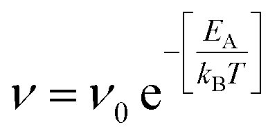 | (1) |
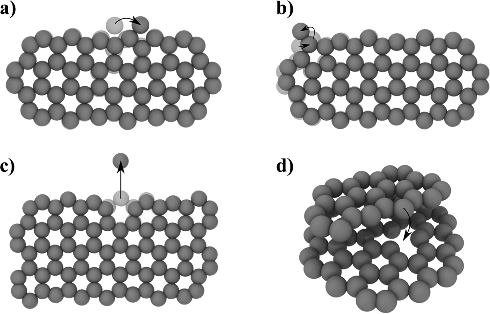 | ||
| Fig. 6 NEB determined activation energies EA for different processes: (a) edge diffusion of an ad-atom (EA = 0.58 eV), (b) 6- to 5-membered ring reconstruction (EA = 1.76 eV), (c) atom removal from a zig-zag edge (EA = 9.17 eV), (d) pinning–depinning process with atom transfer from edge to vacancy (EA,pinning = 0.015 eV < kBT and EA,depinning = 2.47 eV). For detailed energy profiles see ESI Fig. 2.† | ||
The prefactor ν0, which corresponds to a trial rate, can be estimated by the typical frequency of in-plane and out-of-plane optical phonon frequencies of graphene (≈0.45 × 10¹² Hz56). The activation energies EA of 0.58 eV for the edge diffusion process and 1.76 eV for the ring reconstruction process obtained by the NEB calculations (Fig. 6a/b) result in process rates on the order of 109 and 105 Hz respectively at 1200 °C. This indicates that edge diffusion and rearrangement of atoms along the graphene edge are thermally activated processes observable without the influence of the electron beam at the timescale of the experiment. In fact, the frequency is so high, so that we will not be able to image a single defined state of the edge structure in our high temperature in situ TEM experiments.
To understand the observed changes in flake size with time, we carried out NEB calculations, limiting the removal processes to single atoms from a graphene flake in order to maintain computational accessibility. For a mono-atomic process of directly removing an atom from a graphene edge, the NEB calculation yields a high activation barrier of 9.17 eV (Fig. 6c). Compared to the thermal energy kBT of 127 meV at 1200 °C, this leads to a negligible small exponential factor in eqn (1). Thus, the high activation barrier is prohibitive to observe this process just by thermal activation. However, temperature driven atom removal processes are possible, if other reactive species are involved which lower the activation barrier, such as defects in the substrate or hydrogen-cleaved step edges. An example is an atom transfer process to a point defect site (Fig. 6d). Here, the pinning process to the initial bound state has a negligible energy barrier and is thereby mainly limited by the availability of reactive sites. The initial pinning is followed by several rearrangement processes lowering the energy (ESI Fig. 12†). Finally, the depinning process with simultaneous atom loss has a barrier of 2.47 eV, which is thermally accessible under the experimental conditions. This barrier will vary depending on the coordination and nature of the reactive site and can temporarily cause stationary nanoflakes. Single point defects can therefore lead to a continuous shrinkage of a mobile flake, saturating defects along its hopping path. Observed continuous atom loss of stationary flakes involves transfer to reactive step edges, where the high mobility along edges can enable a continuous atom transfer and diffusion. Similarly, an extended defect structure like a line defect or a grain boundary may also act as a possible reactive site for atom transfer and further diffusion. With these results, we believe that highly defective graphene systems can show inherent temperature-driven Ostwald-like ripening even in the absence of electron irradiation.
Apart from providing significant insight in to the high temperature dynamics of ncg, the present results help to understand in detail the pyrolysis of polymers leading to the formation of bulk graphitizing and non-graphitizing carbons. The high-resolution images confirm that fullerene-like structures, previously reported16 in the TEM studies of glassy carbons, are formed by the catalyst-free transformation of amorphous carbon during the pyrolysis. Different types of cage-like structures with varying size and shape are formed during the pyrolysis and, unlike the nanoflakes, these structures seem to be stable and can stay isolated without merging with the active edges. Merging of domains shows that not only the oriented domains can merge laterally but also the misoriented domains can grow by vertical merging. This kind of vertical merging is important in graphitizing carbons, which can be completely graphitized at very high temperatures. Apart from the merging of domains, with the highly defective bulk structure, we think that Ostwald-like ripening can also be a contributing growth mechanism because of the large number of available nearby active sites and diffusion pathways.
Overall, these results show that the high temperature behavior of the nanocrystalline graphene is different from pristine graphene. The high density of defects, carbon nanostructures and active edges greatly influences the dynamics and reactions of the carbon nanostructures and the growth of domains. The growth mechanisms observed are similar to the two well-known growth mechanisms for nanoparticle growth: Smoluchowski ripening, where growth occurs by migration and merging of small clusters57,58 and Ostwald ripening,59 where large clusters grow preferentially by the “dissolution” of small ones. Even though there are reports on migration and merging of carbon nanoflakes/nanostructures on top of graphitic substrates observed inside the TEM,30,53,60,61 there has not been clear experimental evidence for Ostwald ripening in these 2D materials. The main reason for this is probably the high mobility of carbon nanostructures on top of defect-free graphitic substrates, which makes migration and merging favorable, whereas Ostwald ripening is not possible without defects. However, in the present study, as the migration is hindered by pinning and with the presence of a large number of defects, Ostwald ripening can also be observed as a mechanism contributing to the growth of the graphene nanoflakes. As our simulations show, the high activation energy for the direct atom removal from the flake is reduced significantly in the presence of nearby defects and atoms can further diffuse along extended defects, such as reactive edges.
Conclusions
We conducted time resolved HRTEM investigations to unravel the dynamics of nanocrystalline graphene (ncg) during in situ heating. One key outcome of this study is the role of reactive defects and edges, which are present in ncg, on fundamental processes at high temperature. Among others, we analyzed one major graphene growth mechanism – the diffusion of nanoflakes with subsequent lateral merging into larger domains – and identified pinning of the flake to reactive sites along its path as the rate limiting process. Similarly, during vertical merging, when a nanoflake is sliding from a step edge, covalent bonds that are formed between the crossing unsaturated edges slow down the process. Additional to the merging processes, we also observed atom transfer between the structures, in particular an Ostwald-like growth mode, where nanoflakes shrink in favor of larger structures. From our energy barrier calculations, we concluded that defects can lower the activation barrier of an atom transfer process to a value which is accessible in the experimental time frame. Furthermore, in low-dose heating experiments with negligible electron irradiation, we confirmed that the observed processes are inherent temperature-driven processes. It can be summarized, that the high temperature behavior of ncg is fundamentally different from defect-free graphene. The comprehensive analysis of elemental processes during heating of ncg in this work lays an important cornerstone for future improvement of process control, bringing this fabrication method one step closer to industrial application.Conflicts of interest
There are no conflicts to declare.Acknowledgements
CNSK gratefully acknowledges the PhD funding from the Deutscher Akademischer Austauschdienst (DAAD) and MK gratefully acknowledges funding by the High Performance Computing 2 program of the Baden-Württemberg Stiftung (Project “Multi-Skalen-Modellierung von Materialien und Bauelementen für die Energieumwandlung und Energiespeicherung”).References
- K. S. Novoselov, V. I. Fal'ko, L. Colombo, P. R. Gellert, M. G. Schwab and K. Kim, Nature, 2012, 490, 192–200 CrossRef CAS PubMed.
- H. Nguyen Bich and H. Nguyen Van, Adv. Nat. Sci. Nanosci. Nanotechnol., 2016, 7, 1–15 Search PubMed.
- R. S. Edwards and K. S. Coleman, Nanoscale, 2013, 5, 38–51 RSC.
- Z. Zhang, Y. Guo, X. Wang, D. Li, F. Wang and S. Xie, Adv. Funct. Mater., 2014, 24, 835–840 CrossRef CAS.
- S. Sharma, A. Khalajhedayati, T. J. Rupert and M. J. Madou, ECS Trans., 2014, 61, 75–84 CrossRef CAS.
- A. Riaz, F. Pyatkov, A. Alam, S. Dehm, A. Felten, V. S. K. Chakravadhanula, B. S. Flavel, C. Kübel, U. Lemmer and R. Krupke, Nanotechnology, 2015, 26, 325202 CrossRef PubMed.
- Z. Zhang, B. Ge, Y. Guo, D. Tang, X. Wang and F. Wang, Chem. Commun., 2013, 49, 2789–2791 RSC.
- A. Turchanin, D. Weber, M. Büenfeld, C. Kisielowski, M. V. Fistul, K. B. Efetov, T. Weimann, R. Stosch, J. Mayer and A. Gölzhäuser, ACS Nano, 2011, 5, 3896–3904 CrossRef CAS PubMed.
- S.-Y. Son, Y.-J. Noh, C. Bok, S. Lee, B. G. Kim, S.-I. Na and H.-I. Joh, Nanoscale, 2014, 6, 678–682 RSC.
- H. Medina, Y. C. Lin, C. Jin, C. C. Lu, C. H. Yeh, K. P. Huang, K. Suenaga, J. Robertson and P. W. Chiu, Adv. Funct. Mater., 2012, 22, 2123–2128 CrossRef CAS.
- L. A. Pesin, J. Mater. Sci., 2002, 37, 1–28 CrossRef CAS.
- T. G. Desai, J. W. Lawson and P. Keblinski, Polymer, 2011, 52, 577–585 CrossRef CAS.
- P. J. F. Harris, Crit. Rev. Solid State Mater. Sci., 2005, 30, 235–253 CrossRef CAS.
- R. E. Franklin, Proc. R. Soc. London, Ser. A, 1951, 209, 196–218 CAS.
- A. C. Ferrari and J. Robertson, Philos. Trans. R. Soc., A, 2004, 362, 2477–2512 CrossRef CAS PubMed.
- P. J. F. Harris, Philos. Mag., 2004, 84, 3159–3167 CrossRef CAS.
- G. M. Jenkins and K. Kawamura, Nature, 1971, 231, 175–176 CrossRef CAS PubMed.
- R. E. Franklin, Proc. R. Soc. London, Ser. A, 1951, 209, 196–218 CAS.
- S. Jiang, T. Shi, X. Zhan, S. Xi, H. Long, B. Gong, J. Li, S. Cheng, Y. Huang and Z. Tang, J. Micromech. Microeng., 2015, 25, 113001 CrossRef.
- A. W. Robertson, G.-D. Lee, K. He, E. Yoon, A. I. Kirkland and J. H. Warner, Nano Lett., 2014, 14, 1634–1642 CrossRef CAS PubMed.
- O. Lehtinen, I.-L. Tsai, R. Jalil, R. R. Nair, J. Keinonen, U. Kaiser and I. V Grigorieva, Nanoscale, 2014, 6, 6569–6576 RSC.
- J. A. Rodríguez-Manzo, A. V Krasheninnikov and F. Banhart, ChemPhysChem, 2012, 13, 2596–2600 CrossRef PubMed.
- F. Banhart, J. Kotakoski and A. V Krasheninnikov, ACS Nano, 2011, 5, 26–41 CrossRef CAS PubMed.
- H. Yoshida, S. Takeda, T. Uchiyama, H. Kohno and Y. Homma, Nano Lett., 2008, 8, 2082–2086 CrossRef CAS PubMed.
- Z. Liu, Y.-C. Lin, C.-C. Lu, C.-H. Yeh, P.-W. Chiu, S. Iijima and K. Suenaga, Nat. Commun., 2014, 5, 1–7 Search PubMed.
- L. Fei, T. Sun, W. Lu, X. An, Z. Hu, J. C. Yu, R. Zheng, X. Li, H. L. W. Chan and Y. Wang, Chem. Commun., 2014, 50, 826–828 RSC.
- C. N. Shyam Kumar, V. S. K. Chakravadhanula, A. Riaz, S. Dehm, D. Wang, X. Mu, B. Flavel, R. Krupke and C. Kübel, Nanoscale, 2017, 9, 12835–12842 RSC.
- A. W. Robertson, G.-D. Lee, K. He, Y. Fan, C. S. Allen, S. Lee, H. Kim, E. Yoon, H. Zheng, A. I. Kirkland and J. H. Warner, Nano Lett., 2015, 15, 5950–5955 CrossRef CAS PubMed.
- N. Lu, J. Wang, H. C. Floresca and M. J. Kim, Carbon N Y, 2012, 50, 2961–2965 CrossRef CAS.
- B. Westenfelder, J. C. Meyer, J. Biskupek, S. Kurasch, F. Scholz, C. E. Krill and U. Kaiser, Nano Lett., 2011, 11, 5123–5127 CrossRef CAS PubMed.
- J. Choe, Y. Lee, L. Fang, G.-D. Lee, Z. Bao and K. Kim, Nanoscale, 2016, 1–4 Search PubMed.
- A. Chuvilin, U. Kaiser, E. Bichoutskaia, N. a Besley and A. N. Khlobystov, Nat. Chem., 2010, 2, 450–453 CrossRef CAS PubMed.
- A. Chuvilin, U. Kaiser, E. Bichoutskaia, N. a Besley and A. N. Khlobystov, Nat. Chem., 2010, 2, 450–453 CrossRef CAS PubMed.
- T. W. Chamberlain, J. Biskupek, S. T. Skowron, A. V. Markevich, S. Kurasch, O. Reimer, K. E. Walker, G. A. Rance, X. Feng, K. Müllen, A. Turchanin, M. A. Lebedeva, A. G. Majouga, V. G. Nenajdenko, U. Kaiser, E. Besley and A. N. Khlobystov, ACS Nano, 2017, 11, 2509–2520 CrossRef CAS PubMed.
- S. Plimpton, J. Comput. Phys., 1995, 117, 1–19 CrossRef CAS.
- S. J. Stuart, A. B. Tutein and J. A. Harrison, J. Chem. Phys., 2000, 112, 6472–6486 CrossRef CAS.
- G. Henkelman, B. P. Uberuaga and H. Jónsson, J. Chem. Phys., 2000, 113, 9901–9904 CrossRef CAS.
- A. Hjorth Larsen, J. JØrgen Mortensen, J. Blomqvist, I. E. Castelli, R. Christensen, M. Dułak, J. Friis, M. N. Groves, B. Hammer, C. Hargus, E. D. Hermes, P. C. Jennings, P. Bjerre Jensen, J. Kermode, J. R. Kitchin, E. Leonhard Kolsbjerg, J. Kubal, K. Kaasbjerg, S. Lysgaard, J. Bergmann Maronsson, T. Maxson, T. Olsen, L. Pastewka, A. Peterson, C. Rostgaard, J. SchiØtz, O. Schütt, M. Strange, K. S. Thygesen, T. Vegge, L. Vilhelmsen, M. Walter, Z. Zeng and K. W. Jacobsen, J. Phys.: Condens. Matter, 2017, 29, 273002 CrossRef PubMed.
- J. J. P. Stewart, Stewart Comput. Chem., Color. Springs, CO, USA, http://OpenMOPAC.net, 2016 Search PubMed.
- J. J. P. Stewart, J. Mol. Model., 2013, 19, 1–32 CrossRef CAS PubMed.
- A. Stukowski, Modell. Simul. Mater. Sci. Eng., 2010, 18, 015012 CrossRef.
- C. Rubio-Verdú, G. Sáenz-Arce, J. Martinez-Asencio, D. C. Milan, M. Moaied, J. J. Palacios, M. J. Caturla and C. Untiedt, Phys. Chem. Chem. Phys., 2017, 19, 8061–8068 RSC.
- I. V. Lebedeva, A. A. Knizhnik, A. M. Popov, O. V. Ershova, Y. E. Lozovik and B. V. Potapkin, Phys. Rev. B: Condens. Matter Mater. Phys., 2010, 82, 1–10 CrossRef.
- X. Feng, S. Kwon, J. Y. Park and M. Salmeron, ACS Nano, 2013, 7, 1718–1724 CrossRef CAS PubMed.
- A. El-Barbary, H. Telling, P. Ewels, I. Heggie and R. Briddon, Phys. Rev. B: Condens. Matter Mater. Phys., 2003, 68, 1–7 CrossRef.
- A. S. Barnard and I. K. Snook, J. Chem. Phys., 2008, 128, 094707 CrossRef PubMed.
- J. Y. Huang, F. Ding, B. I. Yakobson, P. Lu, L. Qi and J. Li, Proc. Natl. Acad. Sci. U.S.A., 2009, 106, 10103–10108 CrossRef CAS PubMed.
- Z. J. Qi, C. Daniels, S. J. Hong, Y. W. Park, V. Meunier, M. Drndic and A. T. C. Johnson, ACS Nano, 2015, 9, 3510–3520 CrossRef CAS PubMed.
- E. Cisternas and J. D. Correa, Chem. Phys., 2012, 409, 74–78 CrossRef CAS.
- A. W. Robertson, C. S. Allen, Y. a. Wu, K. He, J. Olivier, J. Neethling, A. I. Kirkland and J. H. Warner, Nat. Commun., 2012, 3, 1144 CrossRef PubMed.
- W. Neng, L. Shuang-ying, X. Jun, M. Matteo, Z. Yi-long, W. Shu, S. Li-tao and H. Qing-an, Nanoscale, 2014, 6, 11213–11218 RSC.
- R. F. Egerton, Microsc. Res. Tech., 2012, 75, 1550–1556 CrossRef CAS PubMed.
- A. Barreiro, F. Börrnert, S. M. Avdoshenko, B. Rellinghaus, G. Cuniberti, M. H. Rümmeli and L. M. K. Vandersypen, Sci. Rep., 2013, 3, 1115 CrossRef.
- T. Ma, W. Ren, X. Zhang, Z. Liu, Y. Gao, L.-C. Yin, X.-L. Ma, F. Ding and H.-M. Cheng, Proc. Natl. Acad. Sci. U.S.A., 2013, 110, 20386–20391 CrossRef CAS PubMed.
- S. K. Singh, M. Neek-Amal and F. M. Peeters, J. Chem. Phys., 2014, 140, 074304 CrossRef.
- L. Wirtz and A. Rubio, Solid State Commun., 2004, 131, 141–152 CrossRef CAS.
- C. R. Stoldt, C. J. Jenks, P. A. Thiel, A. M. Cadilhe and J. W. Evans, J. Chem. Phys., 1999, 111, 5157–5166 CrossRef CAS.
- R. A. Budiman and H. E. Ruda, Phys. Rev. B, 2002, 65, 045315 CrossRef.
- S. T. Gentry, S. F. Kendra and M. W. Bezpalko, J. Phys. Chem. C, 2011, 115, 12736–12741 CrossRef CAS.
- M. Jiao, W. Song, H.-J. Qian, Y. Wang, Z. Wu, S. Irle and K. Morokuma, Nanoscale, 2016, 8, 3067–3074 RSC.
- S. Sharma, C. N. Shyam Kumar, J. G. Korvink and C. Kübel, Sci. Rep., 2018, 8, 16282 CrossRef PubMed.
Footnotes |
| † Electronic supplementary information (ESI) available. See DOI: 10.1039/c9na00055k |
| ‡ Presently at Materials Characterization Division, Vikram Sarabhai Space Centre, 695022 Trivandrum, India. |
| This journal is © The Royal Society of Chemistry 2019 |