
 Open Access Article
 This Open Access Article is licensed under a Creative Commons Attribution-Non Commercial 3.0 Unported Licence
The dimensional crossover of quantum transport properties in few-layered Bi2Se3 thin films
Liang
Yang
a,
Zhenhua
Wang
 *ab,
Mingze
Li
ab,
Xuan P. A.
Gao
c and
Zhidong
Zhang
ab
*ab,
Mingze
Li
ab,
Xuan P. A.
Gao
c and
Zhidong
Zhang
ab
aShenyang National Laboratory for Materials Science, Institute of Metal Research, University of Chinese Academy of Sciences, Chinese Academy of Sciences, 72 Wenhua Road, Shenyang, 110016, People's Republic of China
bSchool of Materials Science and Engineering, University of Science and Technology of China, Hefei 230026, China
cDepartment of Physics, Case Western Reserve University, Cleveland, OH 44106, USA. E-mail: zhwang@imr.ac.cn
First published on 17th April 2019
Abstract
Topological insulator bismuth selenide (Bi2Se3) thin films with a thickness of 6.0 quintuple layers (QL) to 23 QL are deposited using pulsed laser deposition (PLD). The arithmetical mean deviation of the roughness (Ra) of these films is less than 0.5 nm, and the root square mean deviation of the roughness (Rq) of these films is less than 0.6 nm. Two-dimensional localization and weak antilocalization are observed in the Bi2Se3 thin films approaching 6.0 nm, and the origin of weak localization should be a 2D electron gas resulting from the split bulk state. Localization introduced by electron–electron interaction (EEI) is revealed by the temperature dependence of the conductivity. The enhanced contribution of three-dimensional EEI and electron–phonon interaction in the electron dephasing process is found by increasing the thickness. Considering the advantage of stoichiometric transfer in PLD, it is believed that the high quality Bi2Se3 thin films might provide more paths for doping and multilayered devices.
Introduction
Topological insulators (TI) are materials with an insulating bulk state (BS) and conducting surface state (SS) which originates from the strong spin–orbit coupling (SOC), and the topological SS is protected by time reversal symmetry (TRS) or lattice symmetries.1–6 The surface band has a linear dispersion relationship near the Dirac point at the high symmetry point.7 Such a SS hosts a massless two dimensional electron gas (2DEG). The most commonly studied three-dimensional (3D) TI with a single Dirac cone and protected by TRS are bismuth telluride (Bi2Te3), antimony telluride (Sb2Te3) and bismuth selenide (Bi2Se3).4,7 The primitive cell of these crystals has five atom layers of A1–B1–A2–B1′–A1′ [where A represents selenium (Se) or telluride (Te), and B represents bismuth (Bi) or antimony (Sb)] stacked along the c axis, defined as one quintuple layer (QL).4 Below a critical thickness for the TIs, the SS opens up a gap at the Dirac point.8 The critical thickness is about 6.0 QL, i.e., about 6 nm for Bi2Se3.9 Magnetic doping or the proximity effect breaks the TRS and opens up a gap at the Dirac point, indicating that it would be possible to use them as on and off switches in spintronics.10 In addition, the Majorana fermions at the interface of the TI and the superconducting materials may be exploited in topological quantum computation.11–13 Because of the theoretical significance and promising applications, the TIs have attracted extensive investigation.The localization of electrons in 2D materials is a classic issue.14,15 Ordinarily the 2D state is localized, whereas the 2D SS of the TI is weakly antilocalized and protected by TRS.16–20 A magnetic field perpendicular to the surface of the TI breaks the TRS, thus the weak antilocalization (WAL) would be broken, leading to negative magnetoconductance (MC).15,21,22 If the WAL is broken or in competition with weak localization (WL), then a positive MC or the transition from a negative to a positive MC will arise. The positive MC in TI films may originate from the magnetic doping of SS or the proximity effect between TI and magnetic materials,23,24 from the gap opened up in TI ultrathin films,25–27 from the 2D bulk sub-bands in ultrathin films,28,29 from 2DEG tied to a surface band bending effect or from the disorder induced by nonmagnetic doping.30,31 In the SS of the TI, the spin-momentum locking leads to the destructive interference, and thus the electrons of the SS exhibit WAL, which leads to higher conductivity at lower temperatures.32 However, at low temperatures, the conductivity of the TI films usually decreases with decreasing the temperature. In the diffusive regime, the conductivity is dominated by the competition of WAL and WL because of the electron–electron interaction (EEI).33–35
To obtain a greater transport contribution from the topological SS, it is important to obtain TI thin films with a high crystallization quality. The methods usually used for preparing TI thin films include molecular beam epitaxy (MBE),33,36–40 chemical vapor deposition,41–44 physical vapor deposition,45–48 pulsed laser deposition (PLD)49–60 and sputtering.61,62 The MBE is the method mainly used to obtain flat and thin TI films for fundamental research, because of its advantages of 2D growth, single crystal yield and easily controlled doping. However, the non-equilibrium process of PLD allows stoichiometric transfer from the target to the film, which gives the possibility of easier doping in TI films.63 The thickness of previously reported TI films deposited by PLD is mostly more than 15 nm, and the arithmetical mean deviation of the roughness (Ra) is mostly larger than 1 nm.49,54,58,59 Therefore, in order to observe the dimensional crossover of the physical properties of the TI materials, it is necessary to prepare thinner TI films with high quality. In a recently published paper on depositing TI films using PLD, the root square mean deviation of roughness (Rq) was decreased to 0.5–0.7 nm, but there existed more than four steps of QL at the surface.60 It is necessary to use flat thin TI film with a large area as the bottom or middle layer of the heterostructure in devices for spintronics.64–67 Investigating better preparation conditions using PLD for TI thin films with flat surfaces is a significant area of research.
This paper reports on the characteristics of Bi2Se3 thin films with a thickness of 6.0–23 QL deposited using PLD. The c-oriented and flat characteristics were determined using X-ray diffraction (XRD) and transmission electron microscopy (TEM). The Ra and Rq of the films were less than 0.5 nm and 0.6 nm, respectively. The positive MC was observed because of the 2DEG introduced by the quantized 2D BS. The EEI correction in the temperature dependence of conductivity is revealed. As the thickness increases, the predominant characteristic of the MC changes from 2D to 3D, and the contribution of the 3D EEI or electron–phonon interaction (EPI) arises. As a result, the dimensional crossover of the quantum transport properties in few-layered Bi2Se3 thin films was successfully revealed.
Experimental method
By changing the deposition time, many samples were prepared using the PLD method. In this research, the focus was on four Bi2Se3 samples with thicknesses of 6.0 QL, 7.0 QL, 9.5 QL and 23 QL on a strontium titanate (SrTiO3) (1 1 1) substrate. These thicknesses ranged from the critical thickness of Bi2Se3 (6.0 QL) to the thickness in which the magnetoresistance of the surface state was too weak to be investigated (23 QL). The surface of the SrTiO3 (1 1 1) was cleaned by plasma before deposition. The substrate was heated to 320 °C under a vacuum greater than 2 × 10⁻⁴ Pa, and then the chamber was charged argon (Ar) until a pressure of 50 Pa was achieved. After keeping the temperature and pressure stable for 5 min, the film was deposited at a laser energy of 400 mJ and a frequency of 1 Hz. The deposition rate was about 12 nm min−1. The deposition temperature used was the best temperature obtained from previous experimentation, which was similar to temperatures mentioned in previous reports of depositing Bi2Se3 films using PLD.68,69 After the deposition, the sample was cooled at a rate of 5 °C min−1 in an atmosphere of Ar gas at 300 Pa, which reduced the vaporization of Se at low pressures. The optimal conditions of the method are those given previously. Another Bi2Se3 sample with a thickness of 6.5 nm was prepared for tuning using the back gate voltage (VG). To decrease the carrier density and strengthen the tuning effect, this sample was deposited at 300 °C. As the conditions of the laser device gradually changed, together with the natural consumption of fluorine gas, to keep the deposition rate the same as that of other samples, the deposition atmosphere of the tuned sample was raised to Ar at 55 Pa.The crystal structure of films was determined using an XRD θ–2θ scan result of (Bruker D8 Advance). The TEM (FEI Tecnai F20) was used for the determination of the structure and interface. The TEM sample for the top view was created by transferring the film to a copper grid. Firstly, poly(methylmethacrylate) (PMMA) was used to cover the surface of a Bi2Se3 sample by spin coating, and then the sample was heated to 180 °C for the chemicals to fuse. Secondly, a blob of epoxy resin, in which a stick was laid, was used to cover the PMMA layer. After the epoxy resin solidified, the stick divided the combination of Bi2Se3/PMMA/epoxy resin. Then the combined sample was immersed in acetone to dissolve the PMMA layer. After a few seconds, the Bi2Se3 layer fell into the acetone and was picked up using a copper grid.
The surface pattern of the samples was measured using atomic force microscopy (AFM, Bruker MultiMode8). Because of the van der Waals contact at the interface of the film and substrate, the film could be easily scratched using a toothpick, and then the difference in height, i.e., the thickness of the film, was measured using AFM. When there were 2 QL steps at the surface of the film, the thickness is defined as the average height of the exposed two steps from the substrate. Where there were 3 QL steps at the surface, the thickness is defined as the height of the middle step from the substrate. The roughness of the samples was calculated using NanoScope Analysis software (Bruker). Electrical measurements were made on samples in the shape of a Hall bar with five terminals. The resistivity and Hall resistance of the samples of various thicknesses were measured using a physical property measurement system (PPMS, Quantum Design) with indium (In) as the contacts. The transport properties of the tuned sample were measured using a home-made electrical property measurement system. Silver paint was used as the gate electrode.
Results and discussion
The crystal structure of Bi2Se3 is illustrated in Fig. 1(a), and Fig. 1(b) shows the structure viewed from the top, along the c axis. One QL and the covalent bonds between the Bi and Se atoms are shown. Fig. 1(c) shows the high resolution transmission electron microscopy (HRTEM) image for the sectional view of the film with a thickness of 6.0 QL, in which the periodic characteristics are observed. The period is 0.96 nm, equal to the thickness of one QL. Because of the preparation process of the TEM samples with mechanical grinding and heating in the air, the surface and the interface which were in contact with the van der Waals forces were partly damaged, thus they are not very clear in the HRTEM image. The bright field image in the top view is shown in Fig. 1(d). During the transmission of electrons with high energy, the sample warps and cracks at the grain boundaries. Thus, the grains are resolvable because of the diffraction contrasts. Fig. 1(e) is the HRTEM image of the zone in the red frame in Fig. 1(d), which includes three grains, and the grain boundaries are marked in orange. The axial vectors a and b of the three grains point to different directions. Fig. 1(f) is the enlarged image of the grain marked as 1, and the fast Fourier transform (FFT) image of it is shown in the inset. The interplanar distance of the (2 2 0) planes were measured and found to be 0.21 nm, from which the value of a in this grain was calculated to be 0.42 nm. The TEM results show the high crystallization quality of the sample.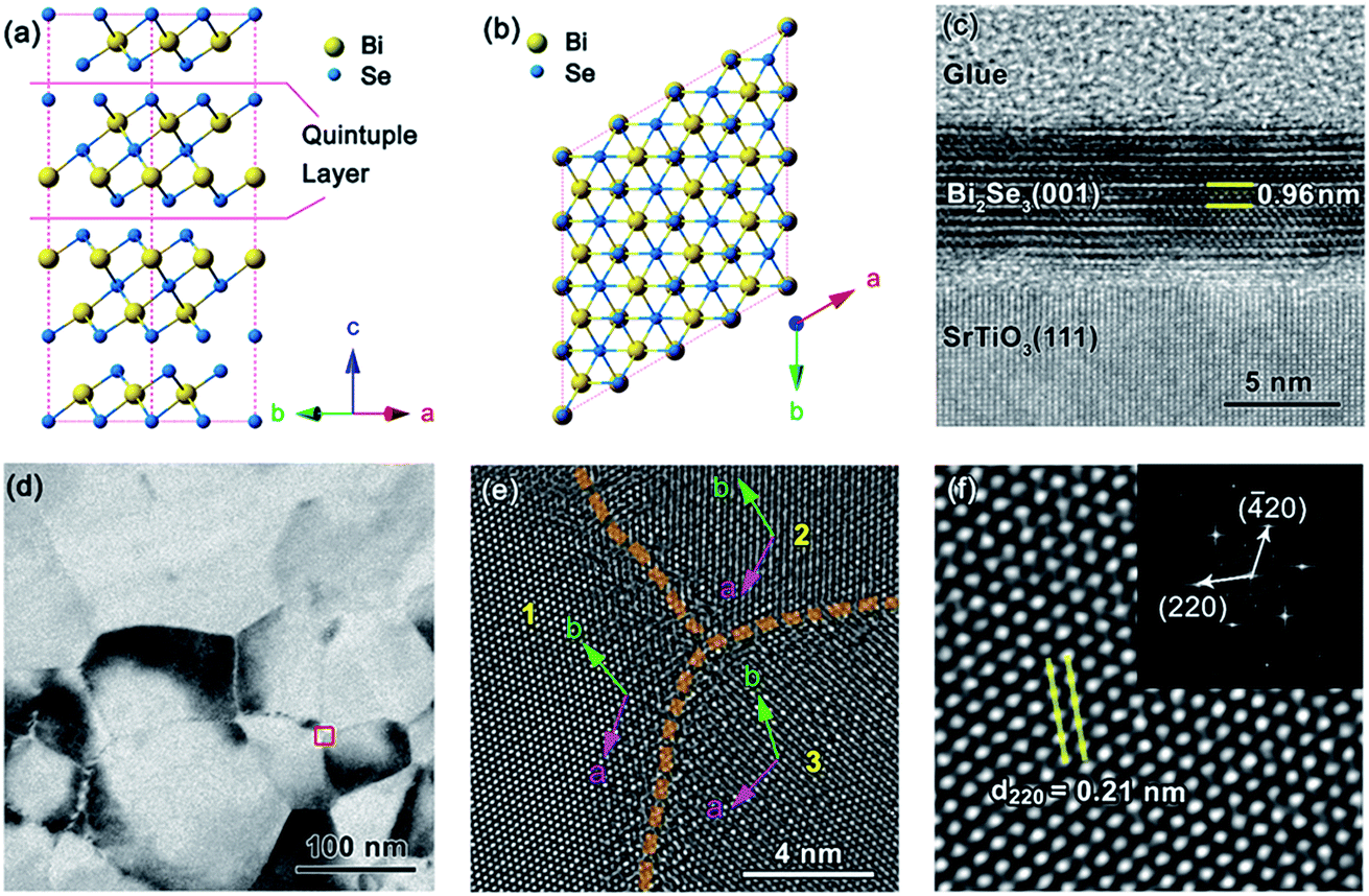 | ||
| Fig. 1 (a) The crystal structure of Bi2Se3. (b) The top view of the structure along the c-axis. (c) HRTEM image of the Bi2Se3 film with a thickness of 6.0 QL on a SrTiO3 substrate. (d) The bright field TEM image view from the top of the film. (e) The HRTEM image of the zone in the red frame in (d). (f) The enlarged HRTEM image of the grain marked as 1 in (e) and its FFT image. | ||
The XRD spectra of the films with different thicknesses are shown in Fig. 2. As shown in Fig. 2(a), all the samples show the (0 0 3n) diffraction peaks of Bi2Se3, indicating a perfect c-orientation of the films. The peaks of In are from the incompletely removed In contacts on the sample after electronic measurement. It is worth noting that clear Kiessig fringes were observed in these samples, which revealed the high homogeneity of the films.70–73 The first order Kiessig peaks moves closer to the (0 0 3n) main peak with increasing thickness, as indicated by the arrows in Fig. 2(b), which shows the enlarged spectra. The XRD results proved that the samples did have a c-oriented Bi2Se3.
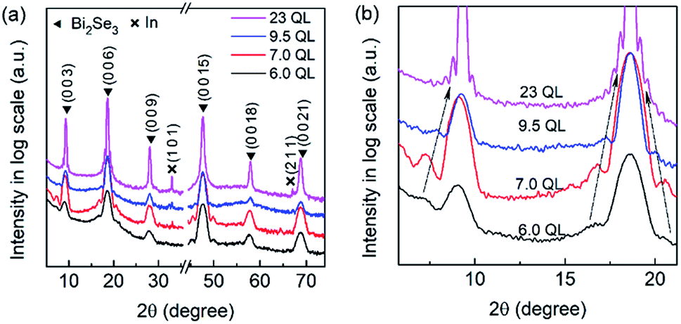 | ||
| Fig. 2 (a) XRD results of Bi2Se3 films. The diffraction peak of the substrate is in the range broken on x-axis. (b) The enlarged spectra of (a). The arrows indicate the position of the first order Kiessig peak. | ||
The AFM measurements were used for investigating the surface condition of the samples of various thicknesses, and the results are shown in Fig. 3. All the films were continuous. The Ra of all the samples was in the range of 0.27–0.45 nm, and the Rq was in the range of 0.38–0.60 nm. In detail, the height profiles of the areas indicated by the blue lines are included below the corresponding 2D images. All four samples were stacked in layers, and the thickness of each layer was about 1 nm, i.e., 1 QL, as measured in the height profiles. At the surface of the film, the difference of height between the highest step and the lowest step was 2 QL. Namely, the Bi2Se3 films near 6 QL with a flat surface feature prepared using PLD. Such a feature is the same for the Bi2Se3 films deposited using MBE,74 and this indicated the potential of PLD for depositing TIs and other layered materials. This provided the chance to observe the intrinsic physical properties of TIs near the critical thickness of the dimensional crossover.
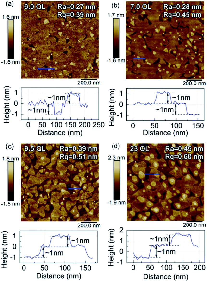 | ||
| Fig. 3 AFM results for the Bi2Se3 samples of (a) 6.0 QL, (b) 7.0 QL, (c) 9.5 QL, and (d) 23 QL. The height profiles of the regions marked by the blue lines are located below the corresponding 2D images. | ||
The dependence of transport properties on temperature and thickness of the samples in zero magnetic field is shown in Fig. 4. The inset of Fig. 4(a) indicates the sample measurement geometry. The resistivity decreases with decreasing temperature from 300 K, then shows an upturn below the transition temperature. The decrease of resistivity below 300 K is considered as the metallic characteristic of the bulk state, attributed to the lack of Se.75,76 The increase of resistivity at low temperatures becomes weaker in thicker samples, indicating the 2D origin of the upturn at low temperatures, as shown in Fig. 4(a). Such a metal-insulator-like transition indicated that the WL was in diffusive mode32,74,77 or a strong localization was in hopping mode,78,79 and this depended on the condition of the sample. The correction of WAL and EEI to the conductivity is given by:45
 | (1) |
![[thin space (1/6-em)]](https://www.rsc.org/images/entities/char_2009.gif) T relationship, which shows linear behavior. Such a linear behavior signifies that the carriers are in the diffusive regime.45,74
T relationship, which shows linear behavior. Such a linear behavior signifies that the carriers are in the diffusive regime.45,74
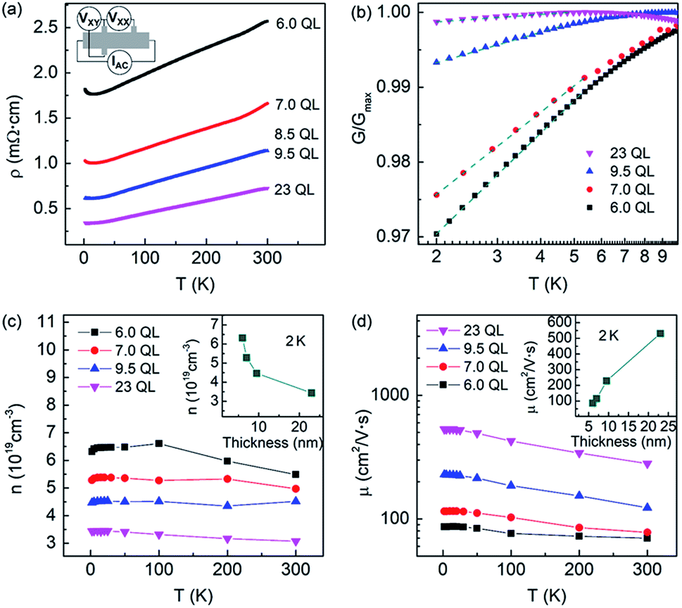 | ||
| Fig. 4 (a) ρ–T relationship of Bi2Se3 samples of various thicknesses. The inset indicates the sample measurement geometry. (b) The temperature dependences of G/Gmax, plotted against lnT. The temperature scale used is 2–10 K. The dashed lines are a guide for the eye. (c) The relationship between n and T of the samples of various thicknesses; the inset is the change of n with samples of different thicknesses at 2 K. (d) The temperature and thickness dependences of μ; the inset is the thickness dependence of μ at 2 K. | ||
In addition, the carrier density (n) and mobility (μ) were calculated and are shown in Fig. 4(c) and (d). The values of n had a negative correlation with thickness, as illustrated in Fig. 4(c) and its inset. This correlation is because of the complicated combination of the carriers from SS and BS or sub-bands of BS. Considering that the Bi:Se ratio of the target is just 2:3, the n of the films could be depressed in the future by adding Se or other elements to the target. Fig. 4(d) gives the temperature and thickness dependences of μ. The μ of thicker films is higher at the same temperature. The inset of Fig. 4(d) illustrates the μ-thickness relationship at 2 K. The value of μ at 2 K increases from 86 cm2 V−1 s−1 to 531 cm2 V−1 s−1 as the thickness increases from 6.0 QL to 23QL. This increase can be attributed to the disappearance of cavities and better crystallization because of the lengthening of the deposition time. The mobility of the samples exceeds the value of most of the Bi2Se3 and Bi2Te3 films deposited using PLD,50,69,80,81 which indicated improved crystal quality.
The magneto-transport property [ΔG = G (H) − G (0)] of the four samples was measured in the range of −7 T to 7 T, and the results are shown in Fig. 5. Obvious cusps were obtained in thinner films near a magnetic field of zero. The cusp was weaker with increasing film thickness or temperature, indicating that the WAL was the origin. In the films with thicknesses of 6.0 QL or 7.0 QL, a positive MC appeared in the high magnetic field range, and was weakened as the thickness increased. Such a phenomenon was also discovered and investigated in Bi2Se3 films deposited using MBE, and was explained by the WL of the quantized BS.29 In the 9.5 QL and 23 QL films, the parabolic characteristic in a high magnetic field range became increasingly obvious with the increasing thickness, for which the MC of BS was responsible.
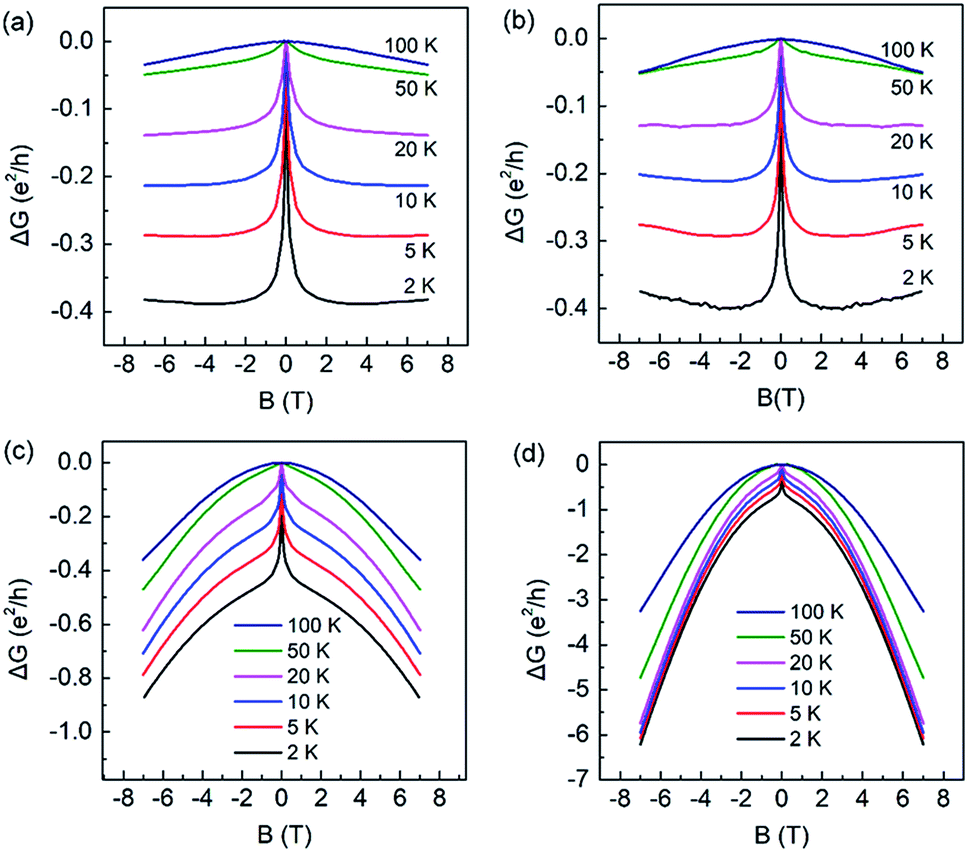 | ||
| Fig. 5 The MC of the Bi2Se3 samples with thicknesses of (a) 6.0 QL, (b) 7.0 QL, (c) 9.5 QL and (d) 23 QL in a perpendicular magnetic field. | ||
The origin of the positive MC was explored by measuring the conductance of four samples in a magnetic field with different directions at 2 K. Fig. 6(a) shows the MC in the perpendicular magnetic field (H⊥). As the thickness increased, the high-field positive MC characteristic disappeared, and the parabolic characteristic emerged. Fig. 6(b) illustrates the MC in the parallel magnetic field (H║). In H║, the negative MC increased as the thickness increased, and a positive MC did not appear. Therefore, it was deduced that the positive MC was an effect in H⊥ and was possibly attributed to the 2DEG from the 2D sub-bands of the quantized BS.28–31
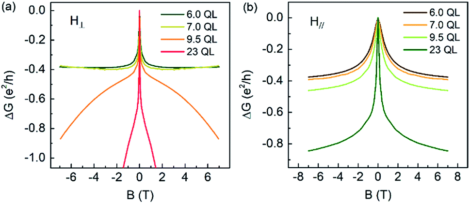 | ||
| Fig. 6 (a) The MC of Bi2Se3 samples with different thicknesses in (a) perpendicular and (b) parallel magnetic fields at 2 K. | ||
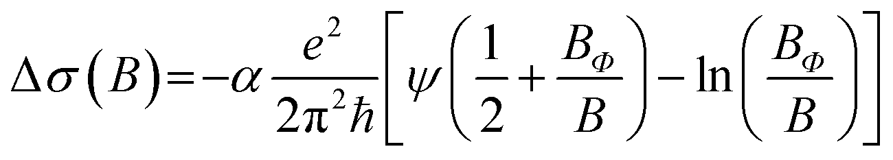
As a TI, the transport of the SS of Bi2Se3 films was analyzed. According to HLN theory,15 in the situation with a strong SOC and no magnetic scattering, the magnetoconductivity in a low field is determined using a simplified equation:15,21,82
 | (2) |
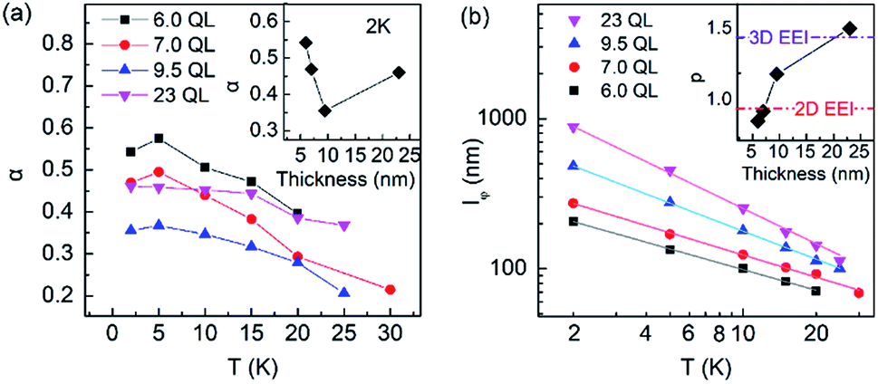 | ||
| Fig. 7 Temperature and thickness dependences of (a) α and (b) lΦ for Bi2Se3 films. The inset of (a) shows the thickness dependence of α at 2 K. The straight lines and the arrow in (b) are the fitted results. The power exponent of lΦ–T−p/2 of Bi2Se3 films with different thicknesses is shown in the inset of (b), in which the dot-dash lines indicate the value of p for 2D EEI and 3D EEI. | ||
The perfect linear dependence of logarithmic lΦ on lnT is shown in Fig. 7(b), which signified the relationship of lΦ ∝ T−p/2. By fitting the data, a monotonically increasing tendency of p with increasing the thickness was obtained, as plotted in the inset of Fig. 7(b). The value of p increased from about 0.91 to near 1.56. The theoretical values of p were 1, 1.5 and 3 corresponding to the dephasing mechanism of 2D EEI, 3D EEI and EPI, respectively.34,77,89 Thus, the tendency of p to increase indicated the enhanced contribution of 3D EEI or EPI in the dephasing process.
To further investigate the transport properties of Bi2Se3 samples deposited using PLD and identify the coupling mechanism, the sample deposited at 300 °C was tuned using a back gate. The Ra and Rq of the sample were 0.30 nm and 0.44 nm, respectively, as shown by the AFM image in the inset of Fig. 8(a). The ρ–T curve of this sample in Fig. 8(a) presents a metallic behaviour at high temperatures and a metal-insulator like transition at about 20 K. The values of n and μ under various VG are calculated and shown in Fig. 8(b). The value of n with VG = 0 V was about 2.6 × 1019 cm−3, lower than that of the samples deposited at 320 °C. This demonstrates that the decreased deposition temperature and increased Ar pressure reduce the amount of Se in the film. For a range of VG from 0 V to −190 V, n decreased from 2.6 × 1019 cm−3 to 1.4 × 1019 cm−3, i.e., the sheet carrier density decreased from 1.5 × 1013 cm−2 to 0.9 × 1013 cm−2, signifying that the Fermi surface was tuned to the bulk condition band edge.85 The value of μ with VG = 0 V was 57 cm2 V−1 s−1, lower by almost half than that for the samples deposited at 320 °C with a similar thickness. This can be attributed to the presence of more cavities and worse crystallization with decreased deposition temperature. The value of μ has a negative correlation with VG, depending on the band structure near the Fermi surface.
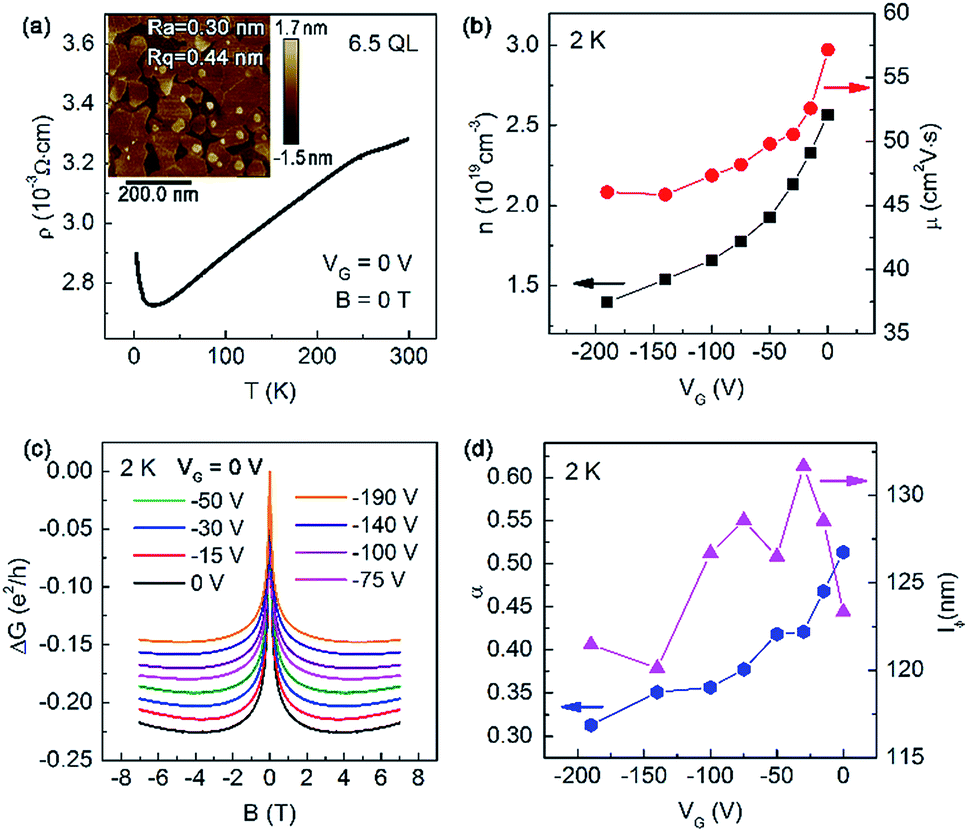 | ||
| Fig. 8 Transport properties and AFM image of the Bi2Se3 sample deposited at 300 °C. (a) ρ–T relationship. The inset shows the AFM image of the sample. (b) n–VG and μ–VG relationships measured at 2 K. (c) VG dependence of MC curves in H⊥ at 2 K. (d) α–VG and lΦ–VG relationship measured at 2 K. | ||
Tuning the MC of the film using VG gives a reasonable interpretation of the α which were less than 1. As shown in Fig. 8(c), the MC curves in H⊥ have a VG dependence. The MC curves show the WAL characteristic in the low magnetic field, and the WL behaviour of positive MC appeared in the high magnetic field range, which was similar to the samples deposited at 320 °C. When the VG was decreased, the width of the cusp in the low H⊥ became larger, and this agreed with the results found in previous investigations.90 As shown in Fig. 8(d), as VG decreased from 0 V to −190 V, α decreased from about 0.51 to 0.31, whereas the change of lΦ was smaller than 10% and fluctuated. Therefore, the larger width of the cusp in low H⊥ was mainly because of the decreased α. In the n-type Bi2Se3 films, a negative VG caused the SS and BS to decouple, resulting in the increased α as the VG decreased.83,84 However, this is the opposite of the α–VG relationship found in this research, which means that the coupling of two SS is the primary mechanism of the α less than 1 in such a thin sample.85 The tuning of the thick samples need more negative VG, which was beyond the ability of the equipment used in this research. For films thick enough to avoid the hybridization of two SS, the primary mechanism may be the coupling of SS and BS.
Conclusions
Bi2Se3 thin films with a (0 0 1) orientation with thicknesses of 6.0–23 QL are prepared using PLD, and their properties were systematically investigated. The Ra and Rq of the films were smaller than 0.5 nm and 0.6 nm, respectively. Steps of QL were observed at the surfaces of all the samples. In the films near the critical thickness, the transition from WAL to WL characteristics appears upon increasing the magnetic field and the WL characteristic disappears upon increasing the thickness. By investigating MC with different directions of magnetic fields, it was determined that the WL characteristic was a 2D effect in H⊥, which was possibly attributed to 2DEG from the 2D sub-bands of BS. It was found that the value of α was less than 0.6, which demonstrated the coupling of two SS for thin samples and the possible coupling of SS and BS for thick samples. In addition, the value of lΦ showed a negative logarithmic dependence on temperature, and increased with increasing thickness. Furthermore, as the thickness increased, the mechanism of the dephasing process gradually changed from simply 2D EEI to including increased 3D EEI or EPI. The observation of dimensional crossover for the quantum transport properties of Bi2Se3 thin films indicated that the PLD was a powerful method for preparing TI thin films of high quality, which is very important for further applications.Conflicts of interest
There are no conflicts to declare.Acknowledgements
This research was supported by the National Natural Science Foundation of China (Grant Nos 51522104, 51331006) and the National Basic Research Program (No. 2017YFA0206302). XPAG thanks the National Science Foundation (DMR-1151534) for financial support.References
- L. Fu, Phys. Rev. Lett., 2011, 106, 106802 CrossRef PubMed.
- G. A. Fiete, Nat. Mater., 2012, 11, 1003 CrossRef CAS PubMed.
- L. Fu and C. Kane, Phys. Rev. B: Condens. Matter Mater. Phys., 2007, 76, 045302 CrossRef.
- H. Zhang, C.-X. Liu, X.-L. Qi, X. Dai, Z. Fang and S.-C. Zhang, Nat. Phys., 2009, 5, 438–442 Search PubMed.
- M. Z. Hasan and C. L. Kane, Rev. Mod. Phys., 2010, 82, 3045–3067 CrossRef CAS.
- X.-L. Qi and S.-C. Zhang, Rev. Mod. Phys., 2011, 83, 1057–1110 CrossRef CAS.
- B. Yan and S.-C. Zhang, Rep. Prog. Phys., 2012, 75, 096501 CrossRef PubMed.
- K. Nakayama, K. Eto, Y. Tanaka, T. Sato, S. Souma, T. Takahashi, K. Segawa and Y. Ando, Phys. Rev. Lett., 2012, 109, 236804 CrossRef CAS PubMed.
- K. He, Y. Zhang, K. He, C.-Z. Chang, C.-L. Song, L.-L. Wang, X. Chen, J.-F. Jia, Z. Fang, X. Dai, W.-Y. Shan, S.-Q. Shen, Q. Niu, X.-L. Qi, S.-C. Zhang, X.-C. Ma and Q.-K. Xue, Nat. Phys., 2010, 6, 584–588 Search PubMed.
- C.-Z. Chang, P. Wei and J. S. Moodera, MRS Bull., 2014, 39, 867–872 CrossRef CAS.
- P. Zareapour, A. Hayat, S. Y. F. Zhao, M. Kreshchuk, A. Jain, D. C. Kwok, N. Lee, S.-W. Cheong, Z. Xu, A. Yang, G. D. Gu, S. Jia, R. J. Cava and K. S. Burch, Nat. Commun., 2012, 3, 1056 CrossRef PubMed.
- W. H. Jiao, S. Jiang, C. M. Feng, Z. A. Xu, G. H. Cao, M. Xu, D. L. Feng, A. Yamada, K. Matsubayashi and Y. Uwatoko, AIP Adv., 2012, 2, 194 Search PubMed.
- E. Wang, H. Ding, A. V. Fedorov, W. Yao, Z. Li, Y.-F. Lv, K. Zhao, L.-G. Zhang, Z. Xu, J. Schneeloch, R. Zhong, S.-H. Ji, L. Wang, K. He, X. Ma, G. Gu, H. Yao, Q.-K. Xue, X. Chen and S. Zhou, Nat. Phys., 2013, 9, 620–624 Search PubMed.
- G. Bergmann, Phys. Rep., 1984, 107, 1–58 CrossRef CAS.
- S. Hikami, A. I. Larkin and Y. Nagaoka, Prog. Theor. Phys., 1980, 63, 707–710 CrossRef.
- Z. H. Pan, E. Vescovo, A. V. Fedorov, D. Gardner, Y. S. Lee, S. Chu, G. D. Gu and T. Valla, Phys. Rev. Lett., 2011, 106, 257004 CrossRef PubMed.
- D. Hsieh, Y. Xia, D. Qian, L. Wray, J. H. Dil, F. Meier, J. Osterwalder, L. Patthey, J. G. Checkelsky, N. P. Ong, A. V. Fedorov, H. Lin, A. Bansil, D. Grauer, Y. S. Hor, R. J. Cava and M. Z. Hasan, Nature, 2009, 460, 1101–1105 CrossRef CAS PubMed.
- S. Souma, K. Kosaka, T. Sato, M. Komatsu, A. Takayama, T. Takahashi, M. Kriener, K. Segawa and Y. Ando, Phys. Rev. Lett., 2011, 106, 216803 CrossRef CAS PubMed.
- Z. Xie, S. He, C. Chen, Y. Feng, H. Yi, A. Liang, L. Zhao, D. Mou, J. He, Y. Peng, X. Liu, Y. Liu, G. Liu, X. Dong, L. Yu, J. Zhang, S. Zhang, Z. Wang, F. Zhang, F. Yang, Q. Peng, X. Wang, C. Chen, Z. Xu and X. J. Zhou, Nat. Commun., 2014, 5, 3382 CrossRef PubMed.
- H. Zhang, C.-X. Liu and S.-C. Zhang, Phys. Rev. Lett., 2013, 111, 066801 CrossRef PubMed.
- J. Chen, X. Y. He, K. H. Wu, Z. Q. Ji, L. Lu, J. R. Shi, J. H. Smet and Y. Q. Li, Phys. Rev. B: Condens. Matter Mater. Phys., 2011, 83, 241304 CrossRef.
- H.-Z. Lu, J. Shi and S.-Q. Shen, Phys. Rev. Lett., 2011, 107, 076801 CrossRef PubMed.
- M. Liu, J. Zhang, C.-Z. Chang, Z. Zhang, X. Feng, K. Li, K. He, L.-L. Wang, X. Chen, X. Dai, Z. Fang, Q.-K. Xue, X. Ma and Y. Wang, Phys. Rev. Lett., 2012, 108, 036805 CrossRef PubMed.
- W. Yang, S. Yang, Q. Zhang, Y. Xu, S. Shen, J. Liao, J. Teng, C. Nan, L. Gu, Y. Sun, K. Wu and Y. Li, Appl. Phys. Lett., 2014, 105, 092411 CrossRef.
- J. Linder, T. Yokoyama and A. Sudbø, Phys. Rev. B: Condens. Matter Mater. Phys., 2009, 80, 205401 CrossRef.
- C.-X. Liu, H. Zhang, B. Yan, X.-L. Qi, T. Frauenheim, X. Dai, Z. Fang and S.-C. Zhang, Phys. Rev. B: Condens. Matter Mater. Phys., 2010, 81, 041307 CrossRef.
- H.-Z. Lu, W.-Y. Shan, W. Yao, Q. Niu and S.-Q. Shen, Phys. Rev. B: Condens. Matter Mater. Phys., 2010, 81, 115407 CrossRef.
- H.-Z. Lu and S.-Q. Shen, Phys. Rev. B: Condens. Matter Mater. Phys., 2011, 84, 125138 CrossRef.
- L. Zhang, M. Dolev, Q. I. Yang, R. H. Hammond, B. Zhou, A. Palevski, Y. Chen and A. Kapitulnik, Phys. Rev. B: Condens. Matter Mater. Phys., 2013, 88, 121103 CrossRef.
- M. Bianchi, D. Guan, S. Bao, J. Mi, B. B. Iversen, P. D. C. King and P. Hofmann, Nat. Commun., 2010, 1, 128 CrossRef PubMed.
- E. P. Amaladass, T. R. Devidas, S. Shilpam and M. Awadhesh, J. Phys.: Condens. Matter, 2017, 29, 175602 CrossRef CAS PubMed.
- H. Z. Lu and S. Q. Shen, Phys. Rev. Lett., 2014, 112, 146601 CrossRef PubMed.
- A. Y. Kuntsevich, A. A. Gabdullin, V. A. Prudkogliad, Y. G. Selivanov, E. G. Chizhevskii and V. M. Pudalov, Phys. Rev. B: Condens. Matter Mater. Phys., 2016, 94, 235401 CrossRef.
- J. Wang, A. M. DaSilva, C.-Z. Chang, K. He, J. K. Jain, N. Samarth, X.-C. Ma, Q.-K. Xue and M. H. W. Chan, Phys. Rev. B: Condens. Matter Mater. Phys., 2011, 83, 245438 CrossRef.
- B. L. Altshuler, A. G. Aronov and D. E. Khmelnitsky, J. Phys. C: Solid State Phys., 1982, 15, 7367–7386 CrossRef CAS.
- C.-Z. Chang, K. He, L.-L. Wang, X.-C. Ma, M.-H. Liu, Z.-C. Zhang, X. Chen, Y.-Y. Wang and Q.-K. Xue, SPIN, 2011, 01, 21–25 CrossRef CAS.
- H.-T. He, G. Wang, T. Zhang, I.-K. Sou, G. K. L. Wong, J.-N. Wang, H.-Z. Lu, S.-Q. Shen and F.-C. Zhang, Phys. Rev. Lett., 2011, 106, 166805 CrossRef PubMed.
- M. Lang, L. He, F. Xiu, X. Yu, J. Tang, Y. Wang, X. Kou, W. Jiang, A. V. Fedorov and K. L. Wang, ACS Nano, 2012, 6, 295–302 CrossRef CAS PubMed.
- A. Roy, S. Guchhait, S. Sonde, R. Dey, T. Pramanik, A. Rai, H. C. P. Movva, L. Colombo and S. K. Banerjee, Appl. Phys. Lett., 2013, 102, 163118 CrossRef.
- J. Dai, W. Wang, M. Brahlek, N. Koirala, M. Salehi, S. Oh and W. Wu, Nano Res., 2015, 8, 1222–1228 CrossRef CAS.
- Z. H. Wang, L. Yang, X. J. Li, X. T. Zhao, H. L. Wang, Z. D. Zhang and X. P. A. Gao, Nano Lett., 2014, 14, 6510–6514 CrossRef CAS PubMed.
- Z. Wang, L. Yang, X. Zhao, Z. Zhang and X. A. Gao, Nano Res., 2015, 8, 2963–2969 CrossRef CAS.
- Z. Sun, B. Man, C. Yang, M. Liu, S. Jiang, C. Zhang, J. Zhang, F. Liu and Y. Xu, Appl. Surf. Sci., 2016, 365, 357–363 CrossRef CAS.
- M. Li, Z. Wang, L. Yang, D. Li, Q. R. Yao, G. H. Rao, X. P. A. Gao and Z. Zhang, Phys. Rev. B: Condens. Matter Mater. Phys., 2017, 96, 075152 CrossRef.
- Y. Jing, S. Huang, K. Zhang, J. Wu, Y. Guo, H. Peng, Z. Liu and H. Q. Xu, Nanoscale, 2016, 8, 1879–1885 RSC.
- H. Zhang, X. Zhang, C. Liu, S. T. Lee and J. Jie, ACS Nano, 2016, 10, 5113–5122 CrossRef CAS PubMed.
- H. Li, J. Cao, W. Zheng, Y. Chen, D. Wu, W. Dang, K. Wang, H. Peng and Z. Liu, J. Am. Chem. Soc., 2012, 134, 6132–6135 CrossRef CAS PubMed.
- J. Barzola-Quiquia, T. Lehmann, M. Stiller, D. Spemann, P. Esquinazi and P. Häussler, J. Appl. Phys., 2015, 117, 075301 CrossRef.
- Y. F. Lee, R. Kumar, F. Hunte, J. Narayan and J. Schwartz, Acta Mater., 2015, 95, 57–64 CrossRef CAS.
- O. Yoshinori, Y. Ryutaro, T. Atsushi, Y. Hongtao, H. Takeaki, I. Yoshihiro, K. Masashi and T. Yoshinori, Appl. Phys. Express, 2011, 4, 083001 CrossRef.
- P. Orgiani, C. Bigi, P. Kumar Das, J. Fujii, R. Ciancio, B. Gobaut, A. Galdi, C. Sacco, L. Maritato, P. Torelli, G. Panaccione, I. Vobornik and G. Rossi, Appl. Phys. Lett., 2017, 110, 171601 CrossRef.
- S. X. Zhang, R. D. McDonald, A. Shekhter, Z. X. Bi, Y. Li, Q. X. Jia and S. T. Picraux, Appl. Phys. Lett., 2012, 101, 202403 CrossRef.
- S.-R. Jian, C.-H. Tasi, S.-Y. Huang and C.-W. Luo, J. Alloys Compd., 2015, 622, 601–605 CrossRef CAS.
- L. Phuoc Huu, P.-T. Liu, C. W. Luo, J.-Y. Lin and K. H. Wu, J. Alloys Compd., 2017, 692, 972–979 CrossRef.
- Y. F. Lee, R. Kumar, F. Hunte, J. Narayan and J. Schwartz, J. Appl. Phys., 2015, 118, 125309 CrossRef.
- A. M. Adam, E. Lilov, V. Lilova and P. Petkov, Mater. Sci. Semicond. Process., 2017, 57, 210–219 CrossRef CAS.
- L. Meng, H. Meng, W. Gong, W. Liu and Z. Zhang, Thin Solid Films, 2011, 519, 7627–7631 CrossRef CAS.
- R. Zeipl, M. Jelinek, M. Vlcek, T. Kocourek, J. Remsa and J. Vanis, Laser Phys., 2015, 25, 015903 CrossRef CAS.
- P. Chaturvedi, B. Saha, D. Saha and S. Ganguly, AIP Conf. Proc., 2016, 1731, 080056 CrossRef.
- C. Bigi, P. Orgiani, A. Nardi, A. Troglia, J. Fujii, G. Panaccione, I. Vobornik and G. Rossi, Appl. Surf. Sci., 2019, 473, 190–193 CrossRef CAS.
- P. Sahu, J.-Y. Chen, J. C. Myers and J.-P. Wang, Appl. Phys. Lett., 2018, 112, 122402 CrossRef.
- W. J. Wang, K. H. Gao and Z. Q. Li, Sci. Rep., 2016, 6, 25291 CrossRef CAS PubMed.
- R. Eason, Pulsed Laser Deposition of Thin Films, John Wiley & Sons, Inc., Hoboken, New Jersey, USA, 2007, p. 28 Search PubMed.
- Y. Wang, D. Zhu, Y. Wu, Y. Yang, J. Yu, R. Ramaswamy, R. Mishra, S. Shi, M. Elyasi, K. L. Teo, Y. Wu and H. Yang, Nat. Commun., 2017, 8, 1364 CrossRef PubMed.
- P. P. Shibayev, E. J. Konig, M. Salehi, J. Moon, M. G. Han and S. Oh, Nano Lett., 2019, 19, 716–721 CrossRef PubMed.
- Y. Hou and R. Wu, Nano Lett., 2019, 19, 2472–2477 CrossRef CAS PubMed.
- S. Cha, M. Noh, J. Kim, J. Son, H. Bae, D. Lee, H. Kim, J. Lee, H. S. Shin, S. Sim, S. Yang, S. Lee, W. Shim, C. H. Lee, M. H. Jo, J. S. Kim, D. Kim and H. Choi, Nat. Nanotechnol., 2018, 13, 910–914 CrossRef CAS PubMed.
- S. X. Zhang, L. Yan, J. Qi, M. Zhuo, Y. Q. Wang, R. P. Prasankumar, Q. X. Jia and S. T. Picraux, Thin Solid Films, 2012, 520, 6459–6462 CrossRef CAS.
- P. H. Le, K. H. Wu, C. W. Luo and J. Leu, Thin Solid Films, 2013, 534, 659–665 CrossRef CAS.
- S. Schreyeck, N. V. Tarakina, G. Karczewski, C. Schumacher, T. Borzenko, C. Brüne, H. Buhmann, C. Gould, K. Brunner and L. W. Molenkamp, Appl. Phys. Lett., 2013, 102, 041914 CrossRef.
- J. M. Hartmann, A. Abbadie and S. Favier, J. Appl. Phys., 2011, 110, 083529 CrossRef.
- X. Leng, J. Pereiro, J. Strle, G. Dubuis, A. T. Bollinger, A. Gozar, J. Wu, N. Litombe, C. Panagopoulos, D. Pavuna and I. Božović, npj Quantum Mater., 2017, 2, 35 CrossRef.
- M. Wang, S. Shen, J. Ni, N. Lu, Z. Li, H. B. Li, S. Yang, T. Chen, J. Guo, Y. Wang, H. Xiang and P. Yu, Adv. Mater., 2017, 29, 1703628 CrossRef PubMed.
- M. Liu, C.-Z. Chang, Z. Zhang, Y. Zhang, W. Ruan, K. He, L.-l. Wang, X. Chen, J.-F. Jia, S.-C. Zhang, Q.-K. Xue, X. Ma and Y. Wang, Phys. Rev. B: Condens. Matter Mater. Phys., 2011, 83, 165440 CrossRef.
- Y. S. Hor, J. G. Checkelsky, D. Qu, N. P. Ong and R. J. Cava, J. Phys. Chem. Solids, 2011, 72, 572–576 CrossRef CAS.
- P. Shang, X. Guo, B. Zhao, X. Dai, L. Bin, J. Jia, Q. Li and M. Xie, Nanotechnology, 2016, 27, 085601 CrossRef PubMed.
- P. A. Lee and T. V. Ramakrishnan, Rev. Mod. Phys., 1985, 57, 287–337 CrossRef CAS.
- J. Liao, Y. Ou, X. Feng, S. Yang, C. Lin, W. Yang, K. Wu, K. He, X. Ma, Q. K. Xue and Y. Li, Phys. Rev. Lett., 2015, 114, 216601 CrossRef PubMed.
- P. A. Lee and D. S. Fisher, Phys. Rev. Lett., 1981, 47, 882–885 CrossRef CAS.
- Y. F. Lee, S. Punugupati, F. Wu, Z. Jin, J. Narayan and J. Schwartz, Curr. Opin. Solid State Mater. Sci., 2014, 18, 279–285 CrossRef CAS.
- P. H. Le, C.-N. Liao, C. W. Luo, J.-Y. Lin and J. Leu, Appl. Surf. Sci., 2013, 285(Part B), 657–663 CrossRef CAS.
- P. E. J. König, P. M. Ostrovsky, I. V. Protopopov, I. V. Gornyi, I. S. Burmistrov and A. D. Mirlin, Phys. Rev. B: Condens. Matter Mater. Phys., 2013, 88, 035106 CrossRef.
- H. Steinberg, J. B. Laloë, V. Fatemi, J. S. Moodera and P. Jarillo-Herrero, Phys. Rev. B: Condens. Matter Mater. Phys., 2011, 84, 233101 CrossRef.
- I. Garate and L. Glazman, Phys. Rev. B: Condens. Matter Mater. Phys., 2012, 86, 035422 CrossRef.
- D. Kim, P. Syers, N. P. Butch, J. Paglione and M. S. Fuhrer, Nat. Commun., 2013, 4, 2040 CrossRef PubMed.
- P. H. Le, S.-P. Chiu, S.-R. Jian, C. W. Luo, J.-Y. Lin, J.-J. Lin, K. H. Wu and M. Gospodinov, J. Alloys Compd., 2016, 679, 350–357 CrossRef CAS.
- N. Bansal, Y. S. Kim, M. Brahlek, E. Edrey and S. Oh, Phys. Rev. Lett., 2012, 109, 116804 CrossRef PubMed.
- A. A. Taskin, S. Sasaki, K. Segawa and Y. Ando, Adv. Mater., 2012, 24, 5581–5585 CrossRef CAS PubMed.
- H.-C. Liu, H.-Z. Lu, H.-T. He, B. Li, S.-G. Liu, Q. L. He, G. Wang, I. K. Sou, S.-Q. Shen and J. Wang, ACS Nano, 2014, 8, 9616–9621 CrossRef CAS PubMed.
- J. Chen, H. J. Qin, F. Yang, J. Liu, T. Guan, F. M. Qu, G. H. Zhang, J. R. Shi, X. C. Xie, C. L. Yang, K. H. Wu, Y. Q. Li and L. Lu, Phys. Rev. Lett., 2010, 105, 176602 CrossRef CAS PubMed.
| This journal is © The Royal Society of Chemistry 2019 |