DOI:
10.1039/C8NA00388B
(Paper)
Nanoscale Adv., 2019,
1, 1853-1863
A green luminescent MoS2–CdTe hybrid nanostructure synthesized through surface charge interaction†
Received
12th December 2018
, Accepted 5th March 2019
First published on 6th March 2019
Introduction
Recently transition metal dichalcogenide (TMDC) quantum dots have been intensively studied because of their superior optical properties.1,2 Transition metal dichalcogenide materials are a new class of materials which are of vivid interest in the fields of semiconductor nanoscience and optoelectronics.3–6 Among metal dichalcogenides, MoS2 quantum dots (QDs) have become a centre of attraction for researchers due to their wide variety of properties in the semiconductor industry for optoelectronic applications and energy harvesting. Contrary to bulk MoS2 which possesses an indirect band gap of 1.2 eV, MoS2 quantum dots show a direct band gap of 1.8 eV,7 giving rise to exotic physicochemical properties for versatile applications viz. electronics, optoelectronics, catalysis, energy storage, etc. Because of their excellent optical properties, superior chemical durability, biocompatibility and lower cytotoxicity, MoS2 QD based systems have also been extensively used as bio-imaging materials.8,9 Apart from MoS2 quantum dots, significant studies have also been performed on a new kind of semiconductor nanocrystal especially II–VI compounds such as CdS, CdSe, CdTe, etc. due to their emission in the visible range.10–12 Among these II–VI semiconductor compounds, CdTe has attracted great interest as it is a direct bandgap material with a bandgap of 1.52 eV which is suitable for emission in the visible spectral range by tuning the size from 1 to 10 nm, generally attributed to the quantum confinement effect.13 CdTe is also being used for photoelectric conversion in solar cells and light emitting diodes as well as in bio-applications.14–16 Moreover, CdTe has many unique electronic and optical properties, such as large absorption cross-section, excellent chemical and photo stability, size-dependent tunability of emission wavelength and narrow emission peak width at half maximum.
Besides these individual quantum dots like MoS2, CdTe, etc., their hybrid structures are also being investigated during the last few years17–22 because of their potential applications viz. photocatalytic, electrocatalytic, photovoltaic, optoelectronic and sensing applications. In the literature, it is well reported that hybrid nanostructures are usually formed using a bottom-up approach and colloidal synthesis. However, to date, synthesis of the hybrid structure using surface charge is the most straightforward route. Although few reports on hybrid structures synthesised by surface charge interaction are already available,23–25 in most cases emission wavelengths of individual components in the hybrid structure do not change corresponding to their bare state. The emission peaks in the hybrid state almost remain in the same position as that of the individual quantum dots. In general, the emission peak of a quantum dot changes significantly depending upon the strength of the interaction with the environment (another quantum dot). Therefore, it is expected to achieve tunable optical properties in the hybrid structure by changing the size of the individual quantum dots and the strength of the interaction between the two quantum dots through surface charge modification. To explore this phenomenon, we have carried out experiments and evaluated whether the resultant emission arises due to the individual quantum dots in solution or a real hybridization of levels occurs between the quantum dots to give a new peak. In the present work, MoS2 with negative surface charge and CdTe with positive surface charge have been synthesised to make a charge-induced hybrid structure MoS2–CdTe. It is already reported that amorphous MoS2 QDs possess a large number of edge defects (‘S’ rich) and thus we have synthesised them to obtain quantum dots with negative surface charge.4 To synthesise positively charged CdTe QDs in an aqueous medium, the hydrophilic capping agent cysteamine is used in acidic medium.26,27 As a result, the surface charge of CdTe QDs becomes positive due to the presence of the –NH3+ moiety. The nature of surface charges of these two individual quantum dots and hybrid ones has been confirmed by zeta potential measurements. The formation of the hybrid structure is confirmed from TEM measurements, DLS measurements, XPS study, zeta potential, photoluminescence emission, UV visible spectroscopy and CV measurements. The tuning of the hybrid level by changing the concentration of CdTe QDs has also been investigated. An interesting fact is that, on increasing the concentration of CdTe, the peak has been blue shifted towards MoS2 emission. However, above a certain MoS2 and CdTe ratio (1![[thin space (1/6-em)]](https://www.rsc.org/images/entities/char_2009.gif) :1), no further peak shift towards MoS2 is observed; rather, the peak is shifted towards CdTe emission which confirms the formation of the hybrid level between MoS2 and CdTe.
:1), no further peak shift towards MoS2 is observed; rather, the peak is shifted towards CdTe emission which confirms the formation of the hybrid level between MoS2 and CdTe.
Moreover, CdTe QDs of three different colors (yellow, green and red) have been prepared to make a hybrid with tunable color. Band positions of the three different CdTe play a vital role in the formation of the hybrid structure. It has been observed that green and yellow CdTe successfully form a hybrid level with MoS2, whereas red CdTe cannot do the same. A detailed study has been carried out on the hybrid structure made from yellow CdTe and MoS2 quantum dots. Cyclic Voltammetry (CV) and absorption measurements have been carried out to calculate the band positions of CdTe and MoS2 quantum dots, and finally, the mechanism of formation of the hybrid structure and its spectroscopic investigation have been depicted successfully.
Experimental section
Materials
Ammonium tetrathiomolybdate (Sigma-Aldrich); hydrazine hydrate (N2H4, Merck); sodium borohydride (NaBH4, Merck); tellurium powder (Te, Sigma-Aldrich); cadmium chloride hemipentahydrate (CdCl2·2.5H2O); hydrochloric acid (HCl, Merck); cysteamine (Sigma-Aldrich), PUR-A-LYZER MEGA DIALYSIS KIT (Sigma-Aldrich); Milli-Q water.
Synthetic procedure
Synthesis of MoS2 quantum dots.
The QDs were synthesised through a bottom-up hydrothermal method by using (NH4)2MoS4. In this procedure, (NH4)2MoS4 was dispersed in 50 mL of water under ultrasonic vibration. Hydrazine hydrate was then added to the above solution for reduction, and the mixture was transferred into a 100 mL Teflon lined steel autoclave and treated hydrothermally at 200 °C for eight hours. After hydrothermal treatment, the solution was dialysed using a PUR-A-LYZER Mega Dialysis kit against Milli-Q water to remove all unreacted chemicals.
Synthesis of cysteamine capped CdTe quantum dots.
Cysteamine capped CdTe QDs were synthesized using CdCl2·2.5H2O and NaHTe. In the first step, NaBH4 and Te powder were taken in a round bottom flask and were mixed in Milli-Q water under an argon atmosphere to synthesize NaHTe. CdCl2·2.5H2O and cysteamine were dissolved in Milli-Q water. The pH of this solution was maintained at 5.5 using the required amount of HCl. The mixture was bubbled by Ar gas to make an O2 free solution. Then the above prepared NaHTe was immediately injected into the reaction mixture under vigorous stirring and it was refluxed at 130 °C in an argon atmosphere. The size of the CdTe QDs can be adjusted by changing the growth time24 (30, 50 and 90 min).
Synthesis of the hybrid nanostructure.
Different hybrid nanostructures were synthesised by mixing the two oppositely charged quantum dots, varying the volumetric ratio of CdTe:MoS2 where the volume of the MoS2 quantum dot solution was kept constant. Simple electrostatic interactions between the two oppositely charged nanoparticles have been used to prepare the hybrid structure.
Characterization
Instrumental details.
To characterize the MoS2 quantum dots, CdTe quantum dots and their hybrid structure, X-ray diffraction (XRD) measurements are carried out on a thick film using an X-ray diffractometer (RICHSEIFERT-XRD 3000P with X-ray Generator-Cu, 10 kV, ten mA, wavelength 1.5418 Å). Microstructural studies are performed using a high-resolution transmission electron microscope (HRTEM). We use a high-resolution transmission electron microscope (HRTEM; JEOL 2100) for microstructural and EDX analysis. The DLS and zeta potential measurements were carried out using a zetasizer nanosystem (Malvern Instruments Ltd). UV-VIS absorption spectra are measured with a Cary UV 5000 spectrophotometer. All the photoluminescence (PL) measurements are performed using a PTI fluoromax QM-400 spectrofluorometer. For the time-correlated single-photon counting (TCSPC) measurements, the samples are excited at 280 and 375 nm using a pico second NANO-LED IBH 280L and 370L. Cyclic voltammetric measurements are carried out under a nitrogen atmosphere using a Ag/Ag+ reference electrode, with a Pt disc as the working electrode and a Pt wire as the auxiliary electrode in a PC-controlled PAR model 273A electrochemistry system using 0.1 M KCl as the electrolyte.
Results and discussion
HRTEM, XRD, DLS and zeta potential of MoS2
TEM measurements have been performed to confirm the structural properties of the as-synthesized MoS2 quantum dots. Fig. 1(a) shows the distribution of the quantum dots. The size distribution plot of the synthesized quantum dots is given in the ESI (Fig. S1†). The SAED pattern (Fig. 1(b)) confirms the amorphous nature of the synthesized QDs. The size distribution of the synthesized amorphous MoS2 QDs is almost 18 nm (shown in Fig. 1(c), from DLS measurements). From the EDX analysis of HRTEM images it is seen that the MoS2 QDs are rich in excess ‘S’ which is attributed to the amorphous nature of the QDs. The EDX analysis in Fig. 1(d) also confirms the formation of molybdenum sulfide quantum dots with a high S/Mo atomic ratio greater than two (∼2.77).28 The surface charge of MoS2 quantum dots is also determined by zeta potential analysis as shown in Fig. 1(e). We have found the zeta potential value of bare MoS2 quantum dots to be negative, −40.8 mV, due to the presence of electronically rich sulfur atoms in the edge of the QDs. To obtain further structural information of amorphous MoS2, we have performed XRD analysis. Due to the presence of a large excess of sulfur defects (‘S’ rich) as shown in HRTEM and zeta potential measurements, we could not find any XRD peak; rather, a broad peak is found corresponding to the amorphous nature of MoS2 QDs, as shown in Fig. 1(f).
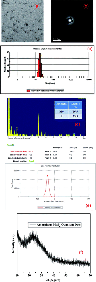 |
| | Fig. 1 (a) TEM image of the as-synthesized MoS2 QDs; (b) SAED pattern of the as-synthesized amorphous MoS2 QDs; (c) particle size distribution of MoS2 QDs from DLS measurements; (d) EDX analysis of sulfur-rich MoS2 QDs; (e) zeta potential of sulfur rich MoS2 QDs; (f) XRD pattern of the as-synthesized amorphous MoS2 QDs. | |
HRTEM, XRD, DLS and zeta potential of CdTe quantum dots
The transmission electron microscope (TEM) image shows different sizes of CdTe quantum dots (Fig. 2). The size distribution plot of different sized quantum dots is given in the ESI (Fig. S2–S4†). The size distribution of yellow emissive CdTe QDs is almost 4 nm. The highly ordered lattice fringes that appeared in high-resolution TEM (HRTEM) images suggest the formation of crystalline CdTe quantum dots as shown in Fig. 3(a). The lattice d-spacing of these quantum dots is found to be 1.41 Å which corresponds to the (200) plane of the crystalline CdTe phase. The corresponding FFT image is also given in the inset of Fig. 3(a). Energy dispersive X-ray spectroscopy (EDX) analysis (given in the ESI, Fig. S5†) also indicates the presence of Cd, Te, C, N and S atoms (the atomic % of carbon is greater due to the usage of the carbon grid). The crystal structure of the as-synthesized cysteamine capped QDs is systematically investigated by X-ray powder diffraction (XRD). From Fig. 3(b), it is seen that the spectra contain some prominent diffraction peaks at 2θ values of 22.3°, 30° and 37.6° which are assigned to the (111), (200) and (220) planes of crystalline CdTe QDs.29–32 All the diffraction peaks are confirmed with JCPDS card no. 24-0513. The surface charge of cysteamine capped CdTe quantum dots is also determined by zeta potential analysis (Fig. 3(c)). The zeta potential value of CdTe QDs is found to be positive, i.e. +23.4 mV, due to the presence of the –NH3+ moiety of the cysteamine ligand in acidic medium at the outer surface of the QDs. The DLS study also shows the size distribution of yellow CdTe (Fig. 3(d)).
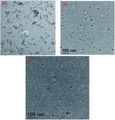 |
| | Fig. 2 (a) TEM images of the as-synthesized green emissive CdTe QDs; (b) yellow emissive CdTe QDs; (c) red emissive CdTe QDs. | |
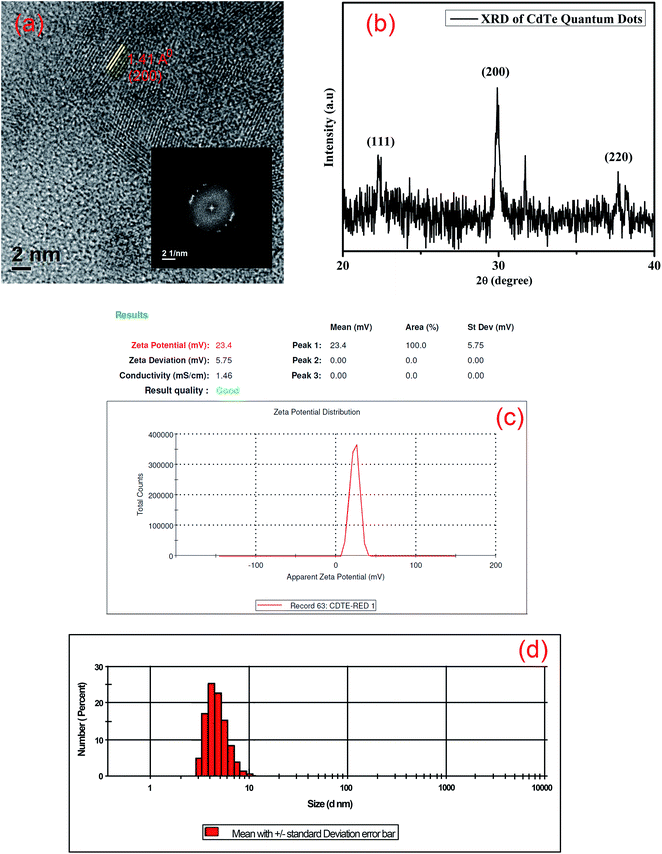 |
| | Fig. 3 (a) High-resolution TEM image and corresponding FFT diagram of CdTe QDs; (b) XRD patterns of CdTe QDs; (c) zeta potential of cysteamine capped CdTe QDs; (d) particle size distribution of CdTe QDs. | |
Hybrid quantum dots
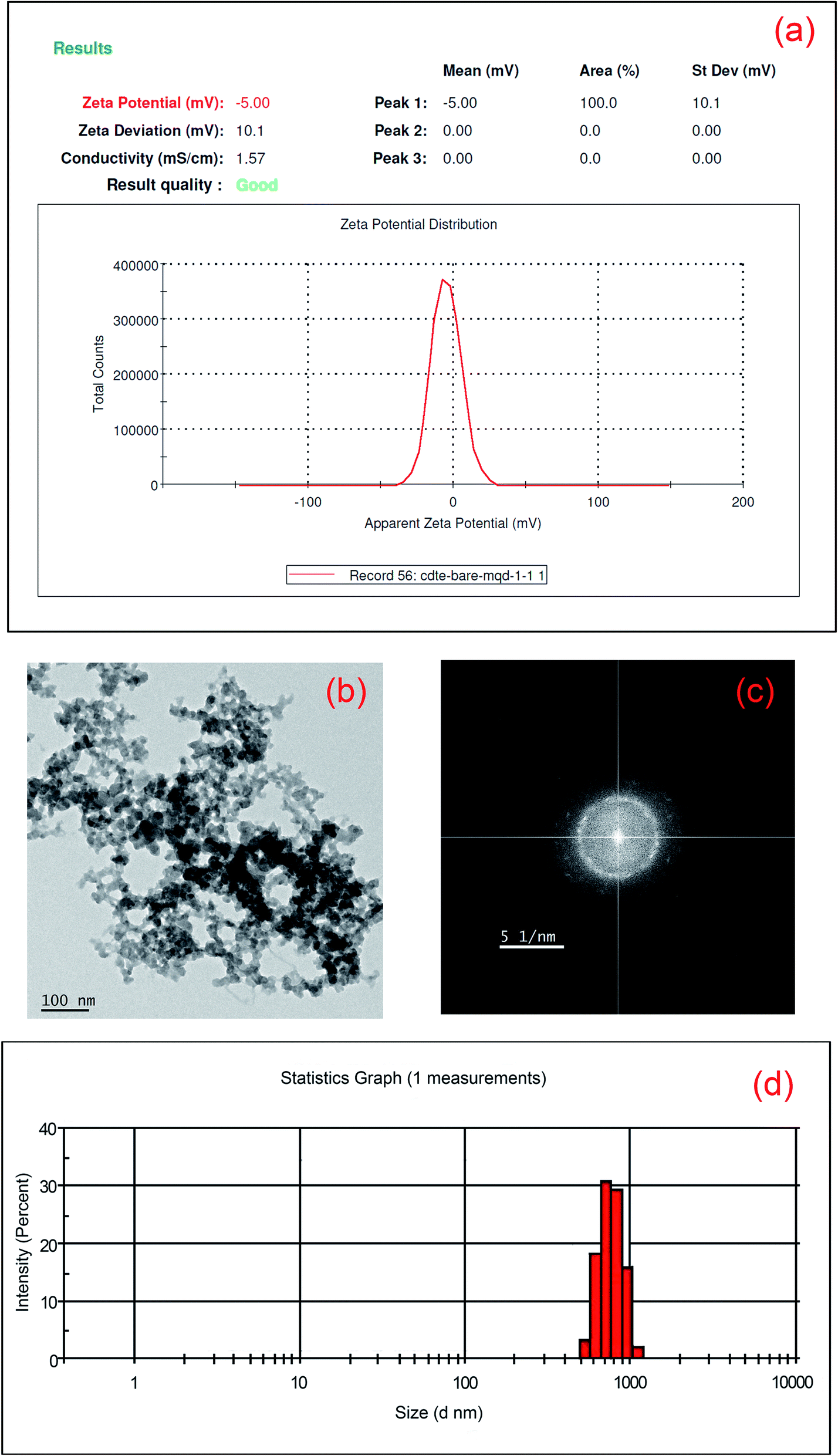
The surface charges of MoS2 and CdTe are found to be −40.8 mV and +23.4 mV respectively from the zeta potential experiment and it is expected that the hybrid structure of the two different QDs is formed through electrostatic interaction when cysteamine capped CdTe QDs are added to the MoS2 QDs. The attachment of the two QDs is confirmed from zeta potential, DLS, corresponding FFT of the hybrid TEM structure and XPS study. The zeta potential of the hybrid structure is found to be −5 mV (shown in Fig. 4(a)) indicating the formation of the hybrid structure. The TEM image of the hybrid structure is shown in Fig. 4(b). As the surfaces of CdTe and MoS2 QDs are totally oppositely charged, each CdTe is surrounded by some MoS2 QDs and each MoS2 QD is surrounded by some CdTe QDs. As a result, a network type structure is formed (Fig. 4(b)). From the FFT image (Fig. 4(c)), presence of crystalline CdTe as well as amorphous MoS2 is also found. From the DLS measurements it is observed that the maximum size of MoS2 QDs is 18 nm, whereas that of yellow emissive CdTe QDs is 4 nm. When CdTe QDs are added to the MoS2 QDs attached nanoparticles are formed with a size of ∼700 nm (shown in Fig. 4(d)) which confirms the network kind structure found in HRTEM images. Moreover, from the shifting of the binding energy of Mo4+, S2− in the hybrid structure also confirms the formation of the hybrid structure (Fig. 5). The peaks for Mo4+-3d5/2, 3d3/2, S2−-2s, S2−-2p3/2, S2−-2p1/2, S22−-2p3/2 and S22−-2p1/2 in bare amorphous MoS2 QDs are found at 228 eV, 232.1 eV, 225.3 eV, 161.4 eV, 162.8 eV, 163.7 eV and 164.3 eV respectively (given in S6†), whereas the peaks of Mo4+-3d5/2, 3d3/2, S2−-2s, S2−-2p3/2, S2−-2p1/2, S22−-2p3/2 and S22−-2p1/2 in the hybrid structure appear at 227.1 eV (0.9 eV), 231.6 eV (0.5 eV), 225 eV (0.3 eV), 160.1 eV (1.3 eV), 160.7 eV (2.1 eV), 161.8 eV (1.9 eV) and 163.5 eV (0.8 eV) respectively (the amount of the shifting of the binding energy value is given in brackets) as shown in Fig. 5(a) and (b). The peaks of nitrogen in –NH3+, Cd-3d5/2 and Cd-3d3/2 in the hybrid one appear at 400.7 eV, 404.5 eV and 411.3 eV respectively as shown in Fig. 5(c). Te-3d5/2 and 3d3/2 arise at 572.4 eV and 575.4 eV and 582.7 eV and 585.9 eV respectively as shown in Fig. 5(d). The higher binding energies, i.e. 575.4 eV and 585.9 eV, confirm the thiolation of the CdTe surface.33 The shifting of the peaks for Mo4+, S2− and S22− towards lower binding energy in the hybrid structure compared to the bare amorphous MoS2 QDs confirms the attachment2,34 between S2− and –NH3+.
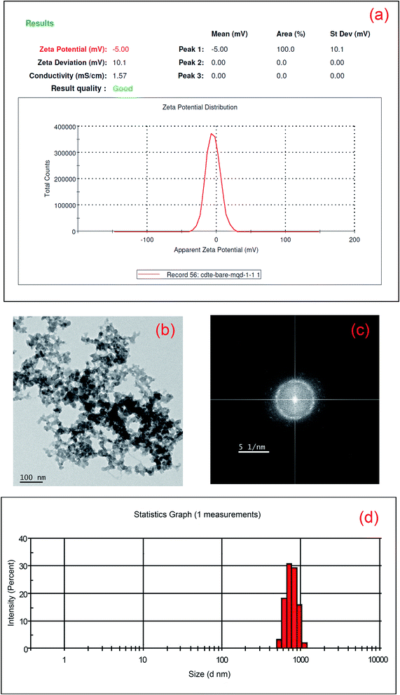 |
| | Fig. 4 (a) Zeta potential of MoS2–CdTe hybrid QDs; (b) high-resolution TEM image of MoS2–CdTe hybrid QDs and (c) corresponding FFT diagram of the hybrid structure; (d) particle size distribution of MoS2–CdTe hybrid QDs. | |
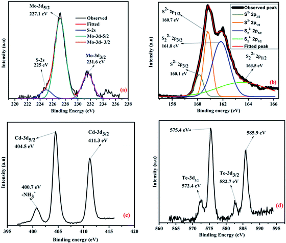 |
| | Fig. 5 (a) XPS spectra of S-2s, Mo(IV)-3d5/2 and 3d3/2 in hybrid QDs; (b) deconvoluted XPS spectra of S2−-2p3/2 and 2p1/2 and S22− 2p3/2 and 2p1/2 in hybrid QDs, (c) XPS spectra of N-1s in –NH3+ attached with the CdTe surface and Cd-3d5/2 and Cd-3d3/2 of hybrid QDs; (d) XPS spectra of Te2−-3d5/2 and 3d3/2 in hybrid QDs. | |
Optical characterization
MoS2 quantum dots.
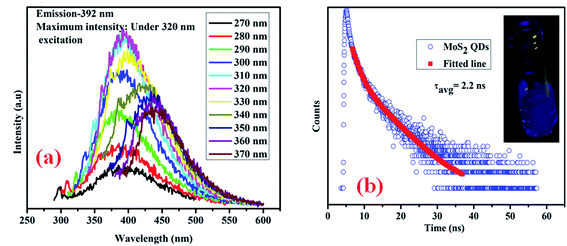
Fig. 6 illustrates the optical properties of the as-synthesized QDs. Fig. 6(a) shows the excitation dependent photoluminescence35,36 (PL) of MoS2 QDs, in which the maximum PL intensity is obtained at 392 nm under 320 nm excitation. Due to the presence of localized defect states (“S” defects), there is a possibility of vibrational relaxation from the conduction band to these localized states, resulting in broadening of the emission spectra. An actual photograph of the blue emission from the MoS2 quantum dots under UV light is shown in the inset of Fig. 6(b). To determine the excited state decay time of the band gap emission, time-resolved emission of the quantum dots is studied, and the spectrum is presented in Fig. 6(b). The excited state decay time of the band gap emission is determined from Fig. 6(b) and found to be 2.2 ns.
 |
| | Fig. 6 (a) Excitation dependent photoluminescence emission spectra of bare MoS2 QDs; (b) time-correlated single photon counting (TCSPC) of the as-synthesized MoS2 QDs and an actual photograph of the emission of bare MoS2 QDs under UV light (inset). | |
CdTe quantum dots.
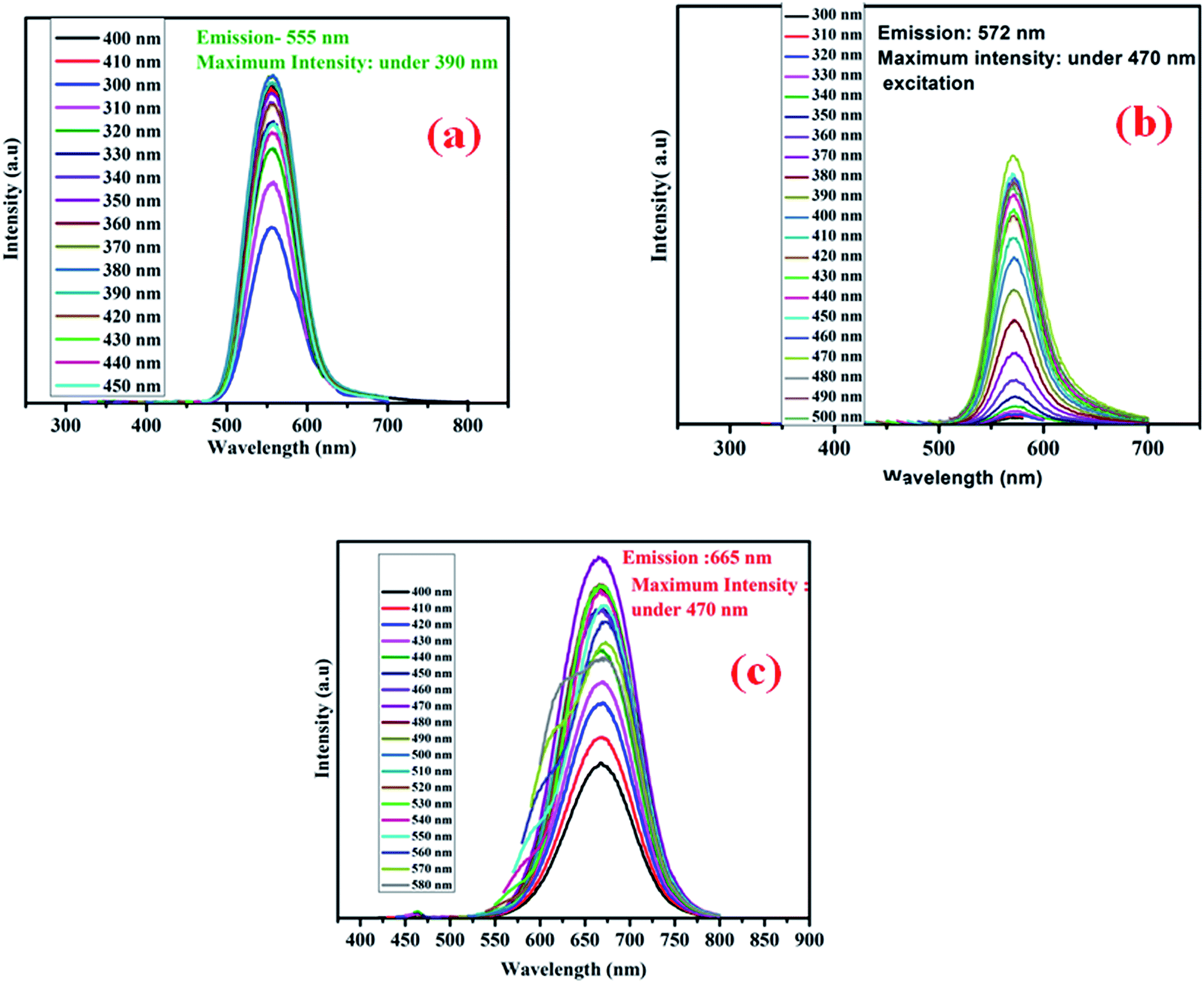
Fig. 7 shows the excitation dependent PL for three different colored CdTe QDs. Green emissive QDs show the maximum PL intensity at 555 nm under 390 nm excitation, yellow emissive QDs show the maximum PL intensity at 572 nm under 470 nm excitation, and for red QDs, it appears at 665 nm under 470 nm excitation.
 |
| | Fig. 7 Excitation dependent photoluminescence emission of (a) green, (b) yellow and (c) red CdTe QDs. | |
Hybrid QDs.
Photoluminescence emission spectra of different hybrid structures composed of yellow CdTe QDs and blue MoS2 QDs are shown in Fig. 8. It is observed that both the peaks of MoS2 and CdTe are present in the PL spectra of all the hybrid structures, where the MoS2 emission peak has very low intensity due to its amorphous nature, whereas the CdTe emission peak is very prominent. There is almost no peak shift for the MoS2, whereas the peak of CdTe is gradually shifted to lower wavelength (towards the MoS2 peak) with increasing the CdTe concentration in the hybrid structure (Fig. 8(a)–(d)).
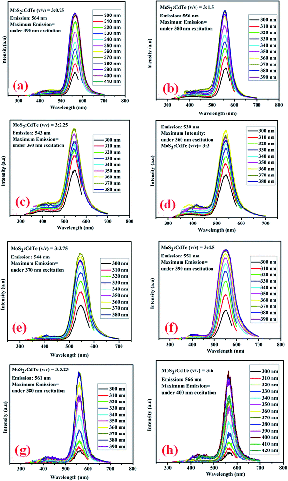 |
| | Fig. 8 (a) Excitation dependent photoluminescence emission spectra of MoS2:CdTe = 3:0.75 (v/v); (b) MoS2:CdTe = 3:1.5 (v/v); (c) MoS2:CdTe = 3:2.25 (v/v); (d) MoS2:CdTe = 3:3 (v/v). (e) Excitation dependent photoluminescence emission spectra of MoS2:CdTe = 3:3.75 (v/v); (f) MoS2:CdTe = 3:4.5 (v/v); (g) MoS2:CdTe = 3:5.25 (v/v); (h) MoS2:CdTe = 3:6 (v/v). | |
MoS2 has a large number of edge sulfur atoms which are electron rich, whereas CdTe quantum dots have been prepared using cysteamine as the capping agent which induces a positive charge on the CdTe surface having –NH3+ at the edge. As a result, when –NH3+ capped CdTe gets closer to electron rich MoS2 quantum dots, they form hybrid structure through simple electrostatic interaction. As the CdTe concentration increases keeping the MoS2 concentration constant, S2− ions present in MoS2 get gradually neutralized by –NH3+ present in CdTe; a new hybrid nanostructure is proposed to form which has a definite set of energy levels, giving rise to new emission peaks as observed for each set of combinations. It is interesting to note that these new emission peaks of the hybrid QDs are at a significantly different position (530 nm for set-IV) and also with a completely different excitation wavelength (360 nm) in comparison to those of pristine CdTe (emission – 572 nm and excitation – 470 nm) and MoS2 QDs (emission – 392 nm and excitation – 320 nm). This new emission is gradually shifted to lower wavelength by increasing the concentration of CdTe. After reaching a certain concentration of CdTe where MoS2:CdTe is 1:1, maximum peak shifting (42 nm, Fig. 8(d)) occurs, indicating complete neutralisation of S2− by NH3+. Beyond this concentration of CdTe, the photoluminescence peak of the hybrid structure again shifts to higher wavelength up to 566 nm (Fig. 8(e)–(h)) which is almost the characteristic emission of yellow CdTe, no further peak shifting occurs beyond this concentration and these results indicate the formation of the hybrid nanostructure. From Time Correlated Single Photon Counting (TCSPC) experiments (Fig. 9), the average life time of the hybrid structure is found to be 16.3 ns.
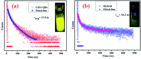 |
| | Fig. 9 (a) Excited state decay profile of cysteamine capped CdTe QDs and an actual photograph of the emission of CdTe QDs under UV light (inset); (b) excited state decay profile of the hybrid structure and an actual photograph of the emission of hybrid QDs under UV light (inset). | |
From the photoluminescence emission spectra of the hybrid structures it is shown that the maximum intensity is observed at 530 nm under 360 nm excitation for 1:1 composition of the hybrid structure (Fig. 8(d)) which is not the excitation wavelength of pristine yellow CdTe QDs as the maximum PL intensity for cysteamine capped yellow CdTe QDs appears under 470 nm excitation (Fig. 7(b)). Therefore, it is confirmed that the emission peak of the hybrid material does not correspond to the emission peak of CdTe or MoS2 but it is a new emission peak which is proposed to originate due to the modulation of the energy band structure by surface charge interaction between MoS2 and CdTe QDs. Apart from photoluminescence, to understand the band positions of MoS2, CdTe and the hybrid structure, cyclic voltammetry (CV) and UV-absorption measurements have been carried out for the 1:1 composition (Fig. S7–S12†). UV peaks for MoS2, CdTe and hybrid structures appear at 350 nm, 508 nm and 358 nm respectively. CV measurements have been performed under an inert atmosphere using three electrode systems at room temperature.
The band positions of pristine MoS2 and CdTe quantum dots and the hybrid MoS2–CdTe nanostructure have been calculated using the following equations:23
where the potential values are in reference to the Ag/Ag
+ reference electrode and Δ
E is the energy difference between the valence band (VB) and the conduction band (CB) measured from their corresponding UV absorption spectra.
From these equations, the valence band and the conduction band of MoS2 are found at −7.24 eV and −3.73 eV respectively, whereas those of CdTe appear at −6.22 eV and −3.82 eV.
Therefore, it is seen that the conduction bands of the two individual quantum dots are very close to each other. Near the conduction band of MoS2, there are large numbers of localized states due to the presence of excess “S2−”. When both MoS2 and CdTe come nearby, there is a possibility for the formation of a hybrid nanostructure due to the electrostatic interaction between S2− and –NH3+. As a result, a new set of energy levels have been formed for the hybrid structure. The schematic diagram of the predicted energy levels is given in Scheme 1. The valence band (at −7.27 eV) is formed which is very near to the MoS2 valence band (−7.24 eV), whereas the conduction band (at −3.81 eV) is formed between the two conduction bands of MoS2 and CdTe and it is very near to the CdTe conduction band (at −3.82 eV). The band diagram is depicted in Scheme 1. With increasing the extent of the volume of CdTe, the edge sulfurs S2− present in the MoS2 QDs are successively get neutralized by –NH3+. So as a result with increasing concentration of CdTe, gradual peak shifting occurs to the lower wavelength region until there is an equal volume of MoS2 and CdTe. After that when the volume of CdTe is again increased, no more S2− remains to be neutralized. Therefore, now the system possesses the character of CdTe only, and as a result, the emission peak becomes red shifted, up to 566 nm (almost characteristic emission of CdTe). So, for the formation of hybrid levels, energy matching of two conduction bands of individual QDs is also necessary. In the case of green CdTe QDs blue shifting also occurs in case of hybridization viz. from 555 nm to 525 nm, whereas due to the energy mismatching of the two conduction levels of red CdTe and MoS2, no peak shifting occurs (Fig. S13 and S14†). Relative fluorescence quantum yields of MoS2, CdTe and hybrid materials are 14.77%, 76.08% and 63.12% respectively from which it is found that the quantum yield of the hybrid materials is much greater than that of MoS2 QDs and comparable to that of CdTe (Fig. S15†).
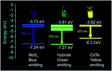 |
| | Scheme 1 Band diagram of MoS2 QDs, capped yellow emissive CdTe QDs and the formed hybrid structure having 1:1 volumetric ratio of individual QDs. | |
Conclusion
A new kind of hybrid nano-structure is synthesized via surface charge interaction of two oppositely charged QDs. Here we have used negatively charged MoS2 QDs and positively charged CdTe QDs. As a result, a new emission peak is observed for the hybrid nano-structure which is different from those of both of the individual QDs. Moreover the excitation wavelength for the hybrid nanostructure is found to be 360 nm which is significantly different to the excitation wavelengths of the individual MoS2 (320 nm) and CdTe QDs (470 nm). This is explained as the formation of a new set of hybrid energy levels from the two QDs during the preparation of the hybrid nanostructure.
Conflicts of interest
There is no conflict of interest to declare.
Acknowledgements
D. H. acknowledges the Council of Scientific and Industrial Research (CSIR), New Delhi, for awarding fellowship, S. B. acknowledges the Indian Association for the Cultivation of Science (IACS) for awarding her fellowship, A. G. acknowledges DST-SERB for his fellowship and S. K. S. acknowledges IACS for infrastructural facilities and the Department of Science and Technology (DST), New Delhi, Government of India, for financial support. We would like to acknowledge Mr Rajib Pramanick for his generous help in the CV study and Mr Manoranjan Bar for his generous help in the TCSPC study.
References
- D. Haldar, D. Dinda and S. K. Saha, J. Mater. Chem. C, 2016, 4, 6321 RSC.
- D. Haldar, A. Ghosh, S. Bose, S. Mondal, U. K. Ghorai and S. K. Saha, Opt. Mater., 2018, 79, 12 CrossRef CAS.
- Z. Lei, W. Zhu, S. Xu, J. Ding, J. Wan and P. Wu, ACS Appl. Mater. Interfaces, 2016, 8, 20900 CrossRef CAS PubMed.
- W. Gu, Y. Yan, C. Zhang, C. Ding and Y. Xian, ACS Appl. Mater. Interfaces, 2016, 8, 11272 CrossRef CAS PubMed.
- W. Dai, H. Dong, B. Fugetsu, Y. Cao, H. Lu, X. Ma and X. Zhang, Small, 2015, 11, 4158 CrossRef CAS PubMed.
- Y. Yan, C. Zhang, W. Gu, C. Ding, X. Li and Y. Xian, J. Phys. Chem. C, 2016, 120, 12170 CrossRef CAS.
- A. Splendiani, L. Sun, Y. Zhang, T. Li, J. Kim, C. Y. Chim, G. Galli and F. Wang, Nano Lett., 2010, 10, 1271 CrossRef CAS PubMed.
- J. Wang, X. Tan, X. Pang, L. Liu, F. Tan and N. Li, ACS Appl. Mater. Interfaces, 2016, 8, 24331 CrossRef CAS PubMed.
- S. Xu, D. Li and P. Wu, Adv. Funct. Mater., 2015, 25, 1127 CrossRef CAS.
- A. K. Bansal, F. Antolini, S. Zhang, L. Stroea, L. Ortolani, M. Lanzi, E. Serra, S. Allard, U. Scherf and I. D. W. Samuel, J. Phys. Chem. C, 2016, 120, 1871 CrossRef CAS.
- K. S. Leschkies, R. Divakar, J. Basu, E. E. Pommer, J. E. Boercker, C. B. Carter, U. R. Kortshagen, D. J. Norris and E. S. Aydil, Nano Lett., 2007, 7, 1793 CrossRef CAS PubMed.
- S. J. Cho, D. Maysinger, M. Jain, B. Roder, S. Hackbarth and F. M. Winnik, Langmuir, 2007, 23, 1974 CrossRef CAS PubMed.
- T. Wang and X. Ziang, ACS Appl. Mater. Interfaces, 2013, 5, 1190 CrossRef CAS PubMed.
- J. Yang and X. Zhong, J. Mater. Chem. A, 2016, 4, 16553 RSC.
- Y. Zheng, S. Gao and J. Y. Ying, Adv. Mater., 2007, 19, 376 CrossRef CAS.
- X. Liu, H. Jiang, J. Lei and H. Ju, Anal. Chem., 2007, 79, 8055 CrossRef CAS PubMed.
- R. M. Clark, B. J. Carey, T. Daeneke, P. Atkin, M. Bhaskaran, K. Latham, I. S. Cole and K. K. Zadeh, Nanoscale, 2015, 7, 16763 RSC.
- P. T. Gomathi, P. Sahatiya and S. Badhulika, Adv. Funct. Mater., 2017, 27, 1701611 CrossRef.
- D. Kufer, I. Nikitsky, T. Lasanta, G. Navickaite, F. H. L. koppens and G. Konstantatos, Adv. Mater., 2015, 27, 176 CrossRef CAS PubMed.
- X. L. Yin, L. L. Li, W. J. Jiang, Y. Zhang, X. Zhang, L. J. Wan and J. S. Hu, ACS Appl. Mater. Interfaces, 2016, 8, 15258 CrossRef CAS PubMed.
- Y. Liu, Y. X. Yu and W. D. Zhang, J. Phys. Chem. C, 2013, 117, 12949 CrossRef CAS.
- S. Hong, D. P. Kumar, E. H. Kim, H. Park, M. Gopannagari, D. A. Reddy and T. K. Kim, J. Mater. Chem. A, 2017, 5, 20851 RSC.
- M. K. Barman, P. Mitra, R. Bera, S. Das, B. Paramanik and A. Patra, Nanoscale, 2017, 9, 6791 RSC.
- S. Kundu, S. Sadhu, R. Bera, B. Paramanik and A. Patra, J. Phys. Chem. C, 2013, 117, 23987 CrossRef CAS.
- R. Bera, S. Mandal, B. Mondal, B. Jana, S. K. Nayak and A. Patra, ACS Sustainable Chem. Eng., 2016, 4, 1562 CrossRef CAS.
- J. Li, T. Yang, W. H. Chan, M. M. F. Choi and D. Zhao, J. Phys. Chem. C, 2013, 117, 19175 CrossRef CAS.
- F. Shi, S. Liu and X. Su, New J. Chem., 2017, 41, 4138 RSC.
- D. Dinda, M. E. Ahmed, S. Mandal, B. Mondal and S. K. Saha, J. Mater. Chem. A, 2016, 4, 15486 RSC.
- Y. Wang and S. Liu, J. Chil. Chem. Soc., 2012, 57, 1109 CrossRef CAS.
- W. H. Yang, W. W. Li, H. J. Dou and K. Sun, Mater. Lett., 2008, 62, 2564 CrossRef CAS.
- F. O. Silva, M. S. Carvalho, R. Mendonca, W. A. Macedo, K. Balzuweit, P. Reiss and M. A. Schiavon, Nanoscale Res. Lett., 2012, 7, 536 CrossRef PubMed.
- R. Wang, B. Li, L. Dong, F. Zhang, M. Fan and L. Zhou, Mater. Lett., 2014, 135, 99 CrossRef CAS.
- Y. Wang, R. Hu, G. Lin, W. C. Law and K. T. Yong, RSC Adv., 2013, 3, 8899 RSC.
- B. K. Gupta, P. Thanikaivelan, T. N. Narayanan, L. Song, W. Gao, T. Hayashi, A. L. M. Reddy, A. Saha, V. Shanker, M. Endo, A. A. Marti and P. M. Ajayan, Nano Lett., 2011, 11, 5227 CrossRef PubMed.
- H. Dong, S. Tang, Y. Hao, H. Yu, W. Dai, G. Zhao, Y. Cao, H. Lu, X. Zhang and H. Zu, ACS Appl. Mater. Interfaces, 2016, 8, 3107 CrossRef CAS PubMed.
- H. Lin, C. Wang, J. Wu, Z. Xu, Y. Huang and C. Zhang, New J. Chem., 2015, 39, 8492 RSC.
Footnotes |
| † Electronic supplementary information (ESI) available. See DOI: 10.1039/c8na00388b |
| ‡ Authors contributed equally. |
|
| This journal is © The Royal Society of Chemistry 2019 |
Click here to see how this site uses Cookies. View our privacy policy here. 
 Open Access Article
 This Open Access Article is licensed under a Creative Commons Attribution-Non Commercial 3.0 Unported Licence
 *
*