
 Open Access Article
 This Open Access Article is licensed under a Creative Commons Attribution-Non Commercial 3.0 Unported Licence
Probing surface states in C60 decorated ZnO microwires: detailed photoluminescence and cathodoluminescence investigations
Joana
Rodrigues
 *a,
Daria
Smazna
b,
Nabiha
Ben Sedrine
a,
Emilio
Nogales
c,
Rainer
Adelung
b,
Yogendra K.
Mishra
b,
Bianchi
Mendez
c,
Maria R.
Correia
a and
Teresa
Monteiro
a
*a,
Daria
Smazna
b,
Nabiha
Ben Sedrine
a,
Emilio
Nogales
c,
Rainer
Adelung
b,
Yogendra K.
Mishra
b,
Bianchi
Mendez
c,
Maria R.
Correia
a and
Teresa
Monteiro
a
aDepartamento de Física & I3N, Universidade de Aveiro, 3810-193 Aveiro, Portugal. E-mail: joana.catarina@ua.pt
bFunctional Nanomaterials, Institute for Materials Science, Kiel University, Kaiserstr. 2, D-24143, Kiel, Germany
cDepartamento de Física de Materiales, Facultad de Ciencias Físicas, Universidad Complutense de Madrid, E-28040 Madrid, Spain
First published on 31st January 2019
Abstract
ZnO microwires synthesised by the flame transport method and decorated with C60 clusters were studied in detail by photoluminescence (PL) and cathodoluminescence (CL) techniques. The optical investigations suggest that the enhanced near band edge recombination observed in the ZnO/C60 composites is attributed to the reduction of the ZnO band tail states in the presence of C60. Well-resolved free and bound excitons recombination, as well as 3.31 eV emission, are observed with increasing amount of C60 flooding when compared with the ZnO reference sample. Moreover, a shift of the broad visible emission to lower energies occurs with increasing C60 content. In fact, this band was found to be composed by two optical centres peaked in the green and orange/red spectral regions, presenting different lifetimes. The orange/red band exhibits faster lifetime decay, in addition to a more pronounced shift to lower energies, while the peak position of the green emission only shows a slight change. The overall redshift of the broad visible band is further enhanced by the change in the relative intensity of the mentioned optical centres, depending on the excitation intensity and on the C60 flooding. These results suggest the possibility of controlling/tuning the visible emission outcome by increasing the C60 amount on the ZnO surface due to the surface states present in the semiconductor. An adequate control of such phenomena may have quite beneficial implications when sensing applications are envisaged.
1. Introduction
Zinc oxide (ZnO) is one of the most studied semiconductor materials owing to its extraordinary physical properties, which are advantageous for a myriad of applications, including optoelectronics, energy and sensing.1–5 Besides the importance of the single wide bandgap oxide semiconductor, ZnO-based composites have gained increasing attention among the international community due to the possibility to extend their scientific and technological uses by enhancing the properties of the combined compounds. Particularly, ZnO-based composites have already demonstrated their advanced multifunctional properties for photocatalytic, chemical and bio-sensing purposes,6–11 to mention just a few fields.To date, the optical properties of bulk and low dimensional ZnO structures have been widely scrutinised.4,12–19 In the case of the luminescence features, the emission of high quality bulk samples is typically characterised by ultraviolet free and bound exciton (FX and D0X) recombination, as well as donor–acceptor pair (DAP) related transitions,4,14,20,21 usually referred as the near band edge recombination (NBE). Moreover, deep level broad emission bands in the green/yellow/red spectral regions are usually observed, although their nature is still a matter of debate in the literature.4,17,22,23 Reducing the dimensions of the crystals towards the nanometre scale leads to changes in the emission spectral features, namely an enlarged NBE, along with broad bands in a wide spectral range18,24,25 that are not necessarily originated from the same optical centres that give rise to bulk luminescence. In fact, in micro- and nanostructures with a high surface to volume ratio, the influence of the surface becomes increasingly important. The presence of interface and/or surface states due to dangling bonds, point defects or surface adsorbed species must be considered to have a potential influence on the material's optical properties. Therefore, when analysing this type of ZnO structure, one should consider that an overlap of emitting centres coming from both bulk and surface defects might occur. These surface-related states can also result in luminescence signatures either in the ultraviolet or in the visible spectral region, as reported for different morphologies at the nanoscale.19,26–29 As a result, in the case of low dimensional structures, surface states assume a decisive role as chemical and bio-probes, as well as in photocatalytic effects.30–33 When compared with the single phase material, ZnO-based composites are expected to lead to changes in the luminescence response either by the presence of additional material's phases or through processes implying cooperative phenomena between the involved materials, such as energy or charge transfer.6–8,34–36 Therefore, the knowledge of the composites' optical properties is a key parameter to boost the development of materials with enhanced and multifunctional properties.
Even though there are already some previous studies concerning ZnO/C60 composites,8,37–43 most of them concentrate on the general characterisation of the materials' properties (mostly structural and morphological) and their possible applications, namely in the field of photocatalysis40,43 or in photovoltaic devices.37,42 Nevertheless, beyond the relevance of applications, a complete knowledge of the fundamental properties of these new materials is also of crucial importance to the understanding of the materials' potentialities for further device development and even to be able to control/tune the desired features. Therefore, herein, we report the detailed optical characterisation of C60 decorated ZnO microwires (MW) through Raman spectroscopy, photoluminescence (PL), room temperature (RT), cathodoluminescence (CL), RT PL excitation (PLE) and time-resolved PL (TRPL), providing new insights into the physical origin of the composites' luminescence mechanisms, namely the role of surface states. ZnO MW were synthesised by the flame transport technique44,45 and further coated with C60 molecules by the drop-casting method.8,46 The optical response of the resulting ZnO/C60 composites is compared with that of the ZnO MW reference sample, enabling to conclude that the effect of increasing C60 flooding allows changing the light outcome, which may enhance the application of such composites for sensing purposes.
2. Experimental details
ZnO MW synthesised by the flame transport method47 were coated with C60 molecules by the drop-casting method as described elsewhere.8,46 In a simple muffle furnace, the precursor materials (Zn microparticles, polyvinyl Butyrol and ethanol in a ratio of 3![[thin space (1/6-em)]](https://www.rsc.org/images/entities/char_2009.gif) :1:2, respectively) were placed in a crucible and burned at 900 °C for 30 minutes. Using a cylindrical ceramic setup, the catcher substrates (typically Si wafer stripes), on which ZnO micro- and nanowires are grown, are mounted on the top facing downwards towards the crucible. During burning, the metallic Zn microparticles are converted into atomic vapour and the growth of micro/nanowires takes place via a solid-vapour-solid (SVS) process in the presence of native oxygen and time, temperature and precursor amounts are the main controlling parameters.45 After the process, the ZnO wires are carefully harvested and then coated with C60 clusters via an indigenously developed drop-casting method.46 A solution is prepared based on commercially available C60 powder and drop casted in portions of ∼50 μL on ZnO MW with a drying step afterwards over several cycles (denoted based on the number of flooding cycles).8
:1:2, respectively) were placed in a crucible and burned at 900 °C for 30 minutes. Using a cylindrical ceramic setup, the catcher substrates (typically Si wafer stripes), on which ZnO micro- and nanowires are grown, are mounted on the top facing downwards towards the crucible. During burning, the metallic Zn microparticles are converted into atomic vapour and the growth of micro/nanowires takes place via a solid-vapour-solid (SVS) process in the presence of native oxygen and time, temperature and precursor amounts are the main controlling parameters.45 After the process, the ZnO wires are carefully harvested and then coated with C60 clusters via an indigenously developed drop-casting method.46 A solution is prepared based on commercially available C60 powder and drop casted in portions of ∼50 μL on ZnO MW with a drying step afterwards over several cycles (denoted based on the number of flooding cycles).8
Two composite samples of C60 covered ZnO MW with two different C60 flooding cycles (#7 and #11 coating cycles), hereafter denoted as ZnO/C60(#7) and ZnO/C60(#11), as well as the ZnO MW reference sample (ZnO), were analysed by Raman, steady-state PL and PLE spectroscopy at RT. Furthermore, temperature dependent (from 11 K to RT) PL measurements were also performed on the three samples using a cold-finger He cryostat. All the PL measurements were carried out exciting the samples with the 325 nm (∼3.81 eV) line of a cw He–Cd laser (power density I0 < 0.6 W cm−2 and beam diameter ∼1 mm). The luminescence radiation was dispersed by using a Spex 1704 monochromator (1 m, 1200 gr mm) and detected with a cooled Hamamatsu R928 photomultiplier. For the excitation power dependence study neutral density filters were applied to the laser excitation. RT PLE experiments were conducted using a Fluorolog-3 Horiba Scientific set-up with a double additive grating Gemini 180 monochromator (1200 gr per mm and 2 × 180 mm) in the excitation mode and a triple grating iHR550 spectrometer in the emission mode (1200 gr per mm and 550 mm). As an excitation source a 450 W Xe lamp was used. The PLE was measured by setting the monochromator at the maxima of the optically active defects and, afterwards, the excitation was scanned to higher energies. TRPL spectra were acquired with the same Fluorolog-3 system using a pulsed Xe lamp coupled to a monochromator, using different time delays for a time window of 10 ms.
The Raman spectra were obtained on a Horiba Jobin Yvon HR800 spectrometer, under the incidence of a 532 nm laser line (Ventus-LP-50085, Material Laser Quantum) and focusing with an objective of ×50 magnification.
Scanning electron microscopy (SEM) characterisation of the samples was performed utilizing a Zeiss Supra 55V with a working voltage of 7–15 kV and a working current of 10 μA. The images reported in the present work were taken in an Inlens/SE – mode, aperture size being kept at 30 μm throughout the measurements.
RT CL measurements were recorded using a Leica Stereoscan 440 microscope system by irradiating the samples with an electron beam under different focusing conditions: with the beam focused on an area in the range of 1 μm2 or severely defocused, irradiating an area with a diameter of several tens of microns, which include several wires. Two different acceleration voltages (3 kV and 5 kV) were used in order to compare the penetration depth dependence of the luminescence spectra with the PL results.
3. Results and discussion
Fig. 1 shows typical SEM micrographs of a single ZnO MW reference sample and the ones decorated with #7 and #11 C60 flooding, ZnO/C60(#7) and ZnO/C60(#11), respectively. The reference ZnO MW sample exhibits a well faceted hexagonal prismatic morphology, while an almost homogeneous C60 surface coating can be observed for the composites. The aspect ratio for the ZnO MW was ≥1:10–1:20 (with the diameter ranging from 8–15 μm and the length estimated to be 100–200 μm). In the used synthesis, variation of the aspect ratios can be achieved through changes in the precursor ratios and the crucible design.47 The ZnO MW are typically grown along the c-axis (as shown in previous studies where the flame transport method was used7,47–50), perpendicularly to the catcher substrate. As earlier reported,39 the wurtzite crystalline nature of the ZnO MW was confirmed via transmission electron microscopy (TEM) and high-resolution TEM (HR-TEM) measurements.47 The spacing between individual microwires (≥20 times the MW's diameter) is large enough for sufficient solution penetration and subsequent surface coverage with C60 molecules. The ZnO MW's surface displays a hydrophilic character which allows for a good wetting of the surface with an aqueous fullerene solution.
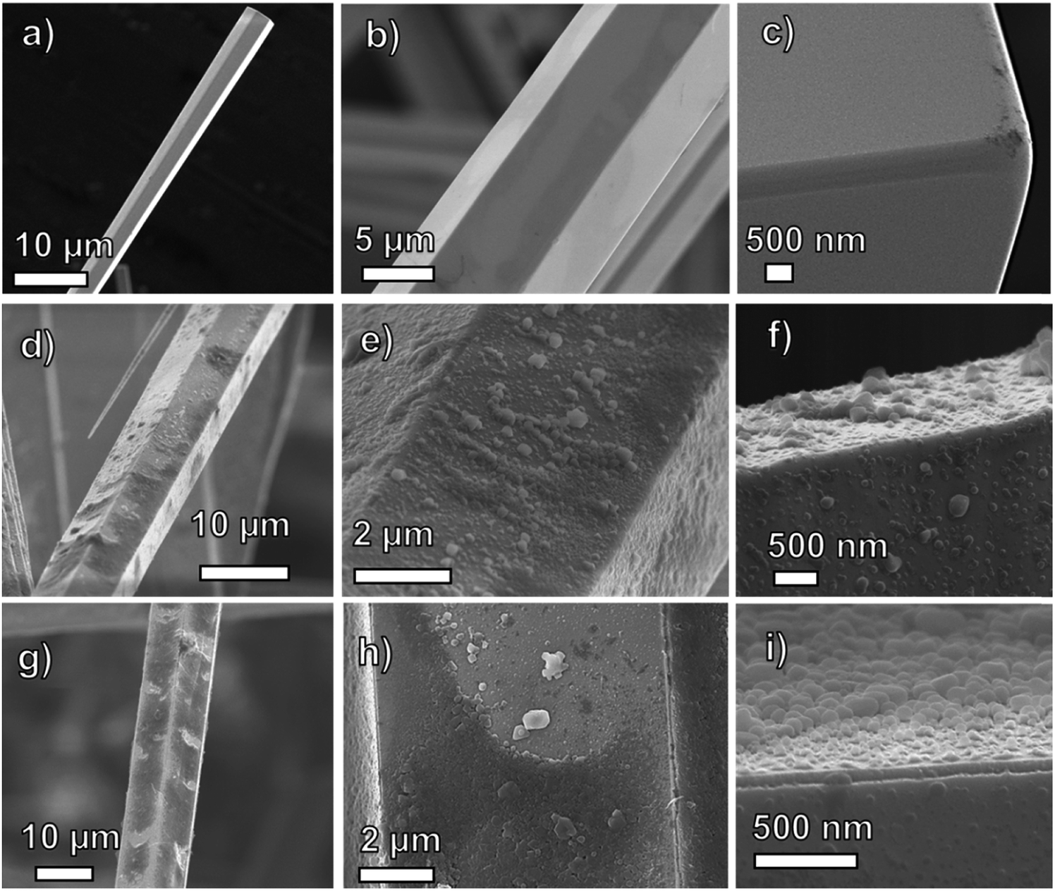 | ||
| Fig. 1 SEM micrographs of the (a–c) ZnO reference, (d–f) ZnO/C60(#7), and (g–i) ZnO/C60(#11) MW samples. | ||
The structural properties of the synthesised samples were assessed by Raman spectroscopy. Fig. 2 depicts the Raman spectra of reference ZnO, ZnO/C60(#7) and ZnO/C60(#11), showing that all the analysed samples exhibit typical vibrational modes of the ZnO hexagonal wurtzite structure that are active in Raman: A1, E1 and E2, as well as their overtones and combined modes.51 The differences observed in the relative intensity of the vibrational modes may arise from polarization effects caused by the different orientations between the ZnO MW and the incidence of the wavevector of the laser beam.52
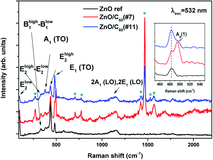 | ||
| Fig. 2 RT Raman spectra of the ZnO reference sample and ZnO/C60(#7) and ZnO/C60(#11) composites obtained in a backscattering configuration and under 532 nm laser excitation. The asterisks denote the modes associated with C60. Inset: enlargement of the E1 (TO) region showing the presence of the C60 Ag(1) mode. | ||
Besides the expected vibrational modes of ZnO, the samples coated with C60 also show some of the normal mode frequencies of an isolated C60 molecule (labelled with an asterisk in Fig. 2).53 Their assignments to the symmetry types are depicted in Table 1. As in the case of ZnO tetrapods covered with C60,8 the most intense Raman mode in the analysed composites is the one peaked at 1469 cm−1, corresponding to a totally symmetric Ag(2) mode.
| Frequency (cm−1) observed in this work | Symmetry type53 |
|---|---|
| 270 | Hg(1) |
| 495 | Ag(1) |
| 705 | Hg(3) |
| 773 | Hg(4) |
| 1422 | Gu(6) |
| 1469 | Ag(2) |
| 1525 | T3u(4) |
| 1570 | Hu(7) |
The luminescence characteristics of the ZnO, ZnO/C60(#7) and ZnO/C60(#11) samples were evaluated at RT by PL, CL, PLE and TRPL. Fig. 3a shows the normalised RT PLE spectra (at the broad band maximum) of the three samples accompanied by the corresponding PL spectra obtained when the samples are excited at above ZnO bandgap energy. Noticeable differences can be identified when a comparison is made between the uncoated and C60 decorated ZnO MW. While the UV recombination (NBE) could not be detected in the ZnO reference sample at this temperature, emission in this spectral region can be seen for the ZnO/C60(#7) and ZnO/C60(#11) composites. Particularly, the NBE emission for the sample coated with the highest flooding clearly shows an asymmetrical spectral shape with a shoulder at ∼3.26 eV and a maximum at ∼3.20 eV (Fig. 3b). The former well matches the expected ZnO bandgap at RT,4 while the latter will be further discussed based on the evolution of the luminescence spectra as a function of temperature. Besides the NBE region, the PL spectra of the samples evidence the presence of broad bands in the green/yellow/red spectral regions. It is worth noting that the relative intensity of the NBE regarding the broad bands is higher for the case of the ZnO/C60(#11) sample. Moreover, increasing the C60 flooding promotes a noticeable redshift of the broad band peak position and a wider full width at half maximum (FWHM) of the overall luminescence, suggesting that additional optical active centres are developed/enhanced upon C60 deposition. Fig. 3c depicts the spectral deconvolution of the broad band for each sample by using two Gaussian functions peaked at ∼2.38 eV (green component) and ∼2.11 eV (orange component). Satisfactory fittings were obtained by considering the same peak position for both components in the different samples, suggesting similar origins. It is clearly observed that the relative intensity of the orange component increases when C60 is added to the surface of the ZnO wires, becoming dominant for the highest flooding. These results indicate that by covering the ZnO surface with C60 molecules several phenomena may occur. One hypothesis is that, by adding C60, one is either promoting the concentration/population of defects that originate the orange emission is promoted due to the materials' interface interaction. Furthermore, a reduction of the defect concentration and/or the paths that lead to the population of the optical centre responsible for the green emission could also occur. The green emission of ZnO (either in bulk, layers or nanostructured samples) is one of the most discussed topics in the literature and a number of different hypotheses have been proposed for its origin.4,17,18,54–56 However, the assignment of the various defect-related emissions observed in ZnO structures to a specific transition is generally complicated by the presence of multiple emissions and broad emission bands comprising the contributions of multiple transitions, making it rather difficult to assess the origin of the observed emissions.24,55 Moreover, it is known that different defects may give rise to emissions in the same spectral range. For instance, Djurišić et al.18,24 claimed that the green band observed in nanostructured samples is originated from defects located at the surface of the semiconductor and suggested that it involves transitions from shallow donor and deep acceptor levels. On the other hand, Zeng et al.55 proposed that, since the excitation of the green emission is usually more efficient at above bandgap energy, its origin is likely related to a transition from the conduction band to deep levels.
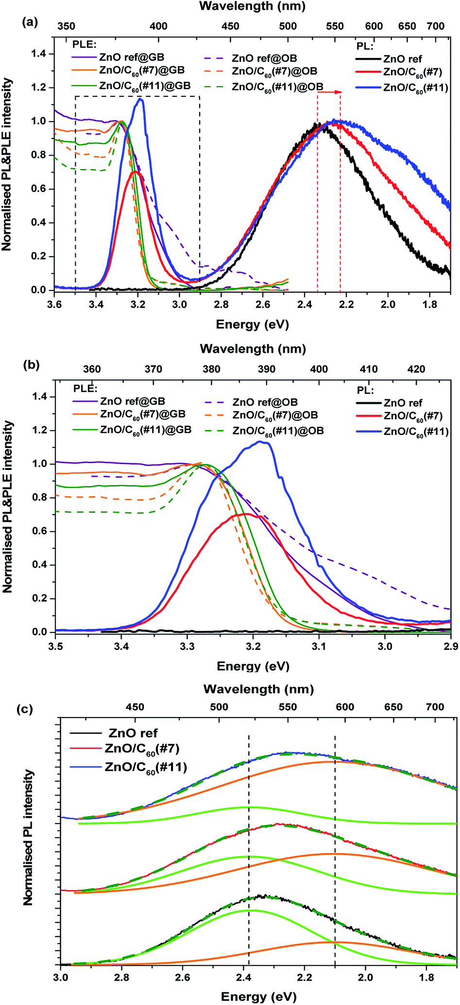 | ||
| Fig. 3 (a) RT PL/PLE spectra monitored at the broad band maxima for the ZnO, ZnO/C60(#7) and ZnO/C60(#11) samples. The PL spectra were obtained with the 325 nm He–Cd laser line and normalised to the broad emission maxima. The PLE spectra are normalised to the excitation maxima. GB and OB stand for green band and orange band, respectively. (b) Expanded spectra of the region marked with the dashed line in (a). (c) Spectral deconvolution of the broad visible bands into two components. An adequate fitting was obtained using two Gaussian functions peaked at ∼2.38 eV and ∼2.11 eV, as described in the text. | ||
In the present case, assuming that the green luminescence is originated from surface defects, placing C60 molecules at the ZnO surface may lead to a passivation of those defects, suppressing the trap-related carriers, therefore leading to a reduction in the intensity of the surface-related green component. As suggested in our previous work on ZnO tetrapods prepared by the same synthesis method and also coated with C60,8 charge transfer between ZnO and C60 may occur in both ways simultaneously, from C60 to ZnO as well as in the opposite direction, and thus reducing the number of carriers that populate the excited states of the green luminescence centre. It is interesting to note that a comparison between the two types of ZnO structures (tetrapods vs. microwires) shows important differences. For instance, in the case of the tetrapods, the NBE emission could only be observed at low temperature, even when covered with the C60 molecules. Moreover, even at 14 K, the UV emission presented a low relative intensity when compared to the visible broad band. The predominance of this band in the tetrapod's structures may originate from surface-related defects, since the surface contribution is expected to be higher in the case of the tetrapods.18,24,57 Also in that case, a slight redshift of the peak position of the broad band was observed by increasing the C60 content from #5 to #20 flooding,8 although less pronounced than that in the present case, which again can be attributed to a higher contribution of the surface-related green emission when compared to the orange component. Additionally, comparing the present results with other results found in the literature for ZnO/C60 composites, it is possible to infer that the decrease in the intensity of the green emission seems to be a common trend, as also reported by Baibarac et al.58 In their work, the authors coated ZnO nanowhiskers with C60 molecules and found that the intensity of the broad band decreases with the C60 addition. Moreover, they observed that in the case of the ZnO nanowhiskers alone, the PL signal decreased when the measurements were carried out in vacuum (∼5.4 × 10⁻⁵ mbar), attributing this behaviour to the removal of physically adsorbed entities on the surface of the semiconductor, reducing the number of trapping centres of electrons and holes. This decrease was not observed in the composites, suggesting the absence of such surface recombination centres, which are expected to be replaced by the chemical attachment of the C60 molecules onto ZnO.58
Nevertheless, it is important to take into account that the behaviour of the ZnO luminescence centres in the presence of different carbon structures may differ from the one presented here, depending on the type of interaction that is established between the carbon and the ZnO structures and the subsequent alignment of the energy levels of both materials, namely the defect-related ones. Furthermore, the origin and locations of the defects found in the semiconductor will also play an important role. For instance, a previous study regarding arrays of vertically aligned carbon nanotubes (CNTs) covered with ZnO structures59 revealed a different behaviour than the one reported in the present paper. In that case, an overall increase of the luminescence, both for the NBE and the green broad emission, was observed. This behaviour was attributed to an enhancement of the intrinsic carriers, promoted by above bandgap excitation photon energy. Moreover, Hu et al.60 also reported the enhancement of the green emission on their nanocrystalline ZnO powders by the addition of different amounts of carbon black, followed by thermal annealing. The authors also claimed that free-carrier concentration increased with the content of carbon black, resulting in high intensity of the green emission in ZnO powder, suggesting that the mechanism responsible for the green emission enhancement is the recombination of the  and electrons with photoexcited holes in the valence band. The involvement of surface states in the observed PL features of the present samples is further corroborated by the used PL excitation conditions (325 nm) which probes essentially the surface of the samples (penetration depth ∼100 nm in ZnO61). The PLE monitored at the maxima of the green (GB) and orange (OB) bands revealed that the preferential paths to populate the broad luminescence are via excitation with photons with energy equal to or higher than the ZnO bandgap, as already observed on the C60 coated ZnO tetrapods.8 As in that case, it is interesting to note that below the bandgap energy a marked excitation tail is observed for the reference sample, especially when monitored in the orange spectral region. Moreover, both samples with the C60 coating follow a trend similar to the one observed for the tetrapods covered with high C60 flooding, namely a steeper ZnO bandgap absorption edge, accompanied by a strong reduction of the band tail states, and a slight shift towards the expected bandgap of pure ZnO. As pointed out for the C60 covered tetrapods,8 the narrowing of the tail states in the composites indicates a suppression of shallow electronic states in the population pathways of the broad emission bands, suggesting that charge transfer from ZnO to C60 should indeed be considered. On the other hand, the samples with steeper absorption show a well-defined NBE recombination and a strong contribution of the emission line associated with surface states (3.31 eV, as corroborated by the low temperature spectra below). In this case, charge transfer from C60 to ZnO is assumed.
Fig. 4a depicts a comparison between the PL results obtained at RT with the CL ones recorded using defocused conditions. Such conditions were employed in order to probe a similar area to the one assessed by PL, comprising several randomly oriented MW. This comparison was made both at 3 kV and at 5 kV with the purpose of evaluating the effect of the penetration depth on the luminescence features; however no significant differences were observed (not shown), and thus the results presented here correspond to an acceleration voltage of 5 kV, which leads to a penetration depth around 200 nm in ZnO. By using defocused conditions, in principle, the penetration depth of the beam can be adjusted in order to be analogous to that employed in the PL measurement. Therefore, similarly to what was observed in the case of PL, the CL spectra evidence the presence of both the NBE and a broad visible band for all samples, although with a different intensity INBE/Ivisible band ratio.
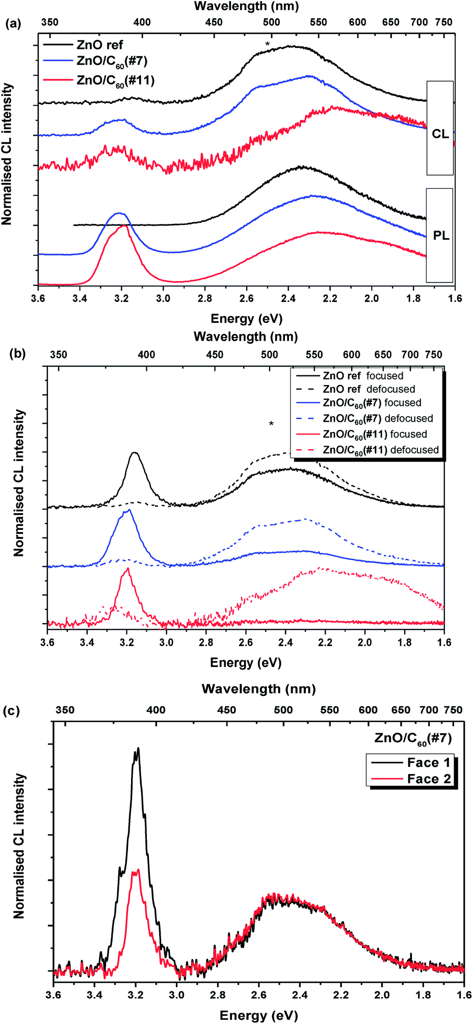 | ||
| Fig. 4 (a) Comparison of the RT PL and CL spectra for the same set of samples. The CL spectra were acquired with an acceleration voltage of 5 kV and under defocused conditions, in order to probe an area similar to the one assessed by PL. (b) RT CL measurement of the ZnO reference, ZnO/C60(#7) and ZnO/C60(#11) samples, obtained at acceleration voltage of 5 kV, comparing focused and defocused conditions. (c) Focused CL spectra obtained on two different faces of a single wire belonging to the ZnO/C60(#7) sample. The small signal depression denoted by the asterisk corresponds to the blaze of the detection grating. | ||
In this case, the visible band dominates the spectra and its spectral shape is slightly different from the one recorded under photon excitation, evidencing a higher contribution from the green component in the case of the reference sample and ZnO/C60(#7) composite. For samples excited with energies higher than the bandgap, differences in the relative intensities and/or widths of the bands usually verified when comparing PL and CL are due to the different excitation densities. For the ZnO/C60(#11) sample mainly the orange emission prevails. In fact, the CL results reveal a similar trend to the one measured by PL, regarding the broadening and redshift of the visible band. Fig. 4b displays the CL spectra obtained for the present set of samples under both focused and defocused conditions, showing a strong influence of this parameter (excitation density) on the relative intensities of the emission features. The CL studies also enabled a more detailed analysis of the luminescence features, as single wires can be easily probed by using focused electron beam conditions, also enabling us to analyse different spots/faces within the same wire. Under such conditions, the relative intensity of the NBE emission was seen to become much higher than the visible band, dominating the CL spectra even for the reference sample where no NBE was detected in the case of PL at this temperature. For the case of the ZnO/C60(#11) composite, the visible band almost disappears and mostly the NBE recombination is detected. The excitation density is known to strongly affect the relative intensities of the luminescence bands, which is normally due to differences in the transition probabilities of the optical centres. In PL measurements, an increase of the NBE band intensity with respect to the visible bands was also observed when increasing the excitation density (not shown). This effect can even induce band luminescence quenching, such as the one observed in the CL spectrum for the broad visible band in the ZnO/C60(#11) sample obtained with the focused electron beam, Fig. 4b. Moreover, the peak position of the NBE emission was seen to slightly vary depending on the probed sample. In the case of the reference sample, this emission is centred at ∼3.16 eV, while for the composite samples ZnO/C60(#7) and ZnO/C60(#11) the maxima are located at ∼3.19 eV and ∼3.20 eV, respectively, in line with what was observed in PL. Indeed, the RT PL and CL of the composites can be seen as an overlap of two main maxima at ∼3.26 eV and ∼3.20 eV with different relative intensities. The peak observed at ∼3.26 eV corresponds to the overlap of the FX and 3.31 eV recombination and the one at ∼3.20 eV is due to the overlap of the LO phonon replicas, as will be shown below by the temperature dependence study performed on the NBE emission for the composite samples. It is also worth noting that the INBE/Ivisible band ratio of these samples is dependent on the probed wire facet (see an example in Fig. 4c for the ZnO/C60(#7) sample), which can be associated with different densities of C60 covering each facet. In fact, this is likely to occur due to the employed composite preparation, which may lead to total or partially uncoated facets. Nevertheless, the spectral shape and peak position of both emissions are analogous for the two probed faces.
The behaviour of the broad emission bands was further explored by power-dependent PL measurements applying neutral density filters to the laser excitation, as depicted in Fig. 5. In the case of the samples with C60, the peak position of the band maxima revealed a shift towards lower energies with decreasing excitation density, while for the reference sample (Fig. 5a) no significant shift was detected.
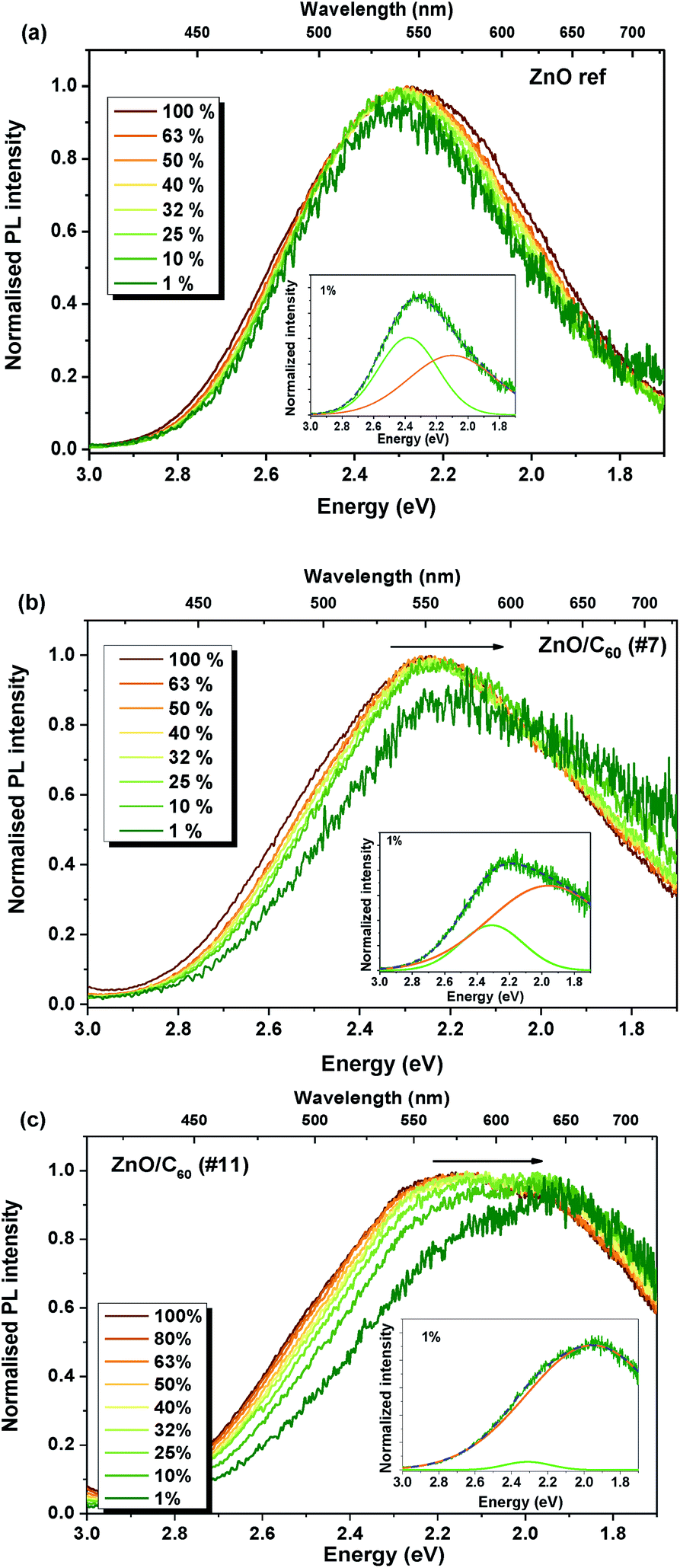 | ||
| Fig. 5 RT power-dependent PL spectra of the (a) reference, (b) ZnO/C60(#7) and (c) ZnO/C60(#11) samples. Insets: spectral deconvolution of the broad band when excited with 1% of the initial laser beam power density, showing the predominance of the orange/red emission. | ||
As previously discussed, the broad band is composed by two optical centres, whose relative intensity was seen to change with the decrease of the excitation power in the case of the composite samples. As the power excitation decreases, the relative intensity of the centre in the orange/red spectral region becomes higher than that of the green emission, resulting in the pronounced shift of the broad band towards lower energies. This dominance of the orange/red emission over the green one is well evidenced by the spectral deconvolution of the band when excited with low power (1% of the initial one), as shown in the insets of Fig. 5b and c. Besides the change in the relative intensity, the spectral deconvolution also enabled us to observe that both green and orange/red components exhibit a shift towards lower energies by reducing the excitation density, contributing to the redshift of the overall luminescence. In the first case, the peak position changes from 2.38 eV to 2.31 eV in both composites, while the orange/red emission shifts from 2.11 eV to 1.96 eV. This behaviour is typical for DAP centres, where the recombination probability is dependent on the distance between the donor and acceptor species.62,63 When low excitation densities are applied, only part of the donors and acceptors are excited. As the power increases, more donors and acceptors become excited until reaching the saturation condition where all the pairs are excited. This leads to an additional contribution from the closest pairs with higher transition probability to the recombination spectra, resulting in the shift of the emission to higher energy with an increase in the excitation density.62,63 The different behaviour found for the reference sample with respect to the composite samples may be attributed to the interaction of the defects that give rise to these luminescent centres with the C60 molecules.
The presence of the two optical centres is also evident in the time-resolved PL study. Fig. 6 displays a comparison between the steady-state and the time-resolved spectra (acquired with a time delay of 0.05 ms) for the composites. Comparing the two spectra for each sample it is clear that the low energy component of the broad band almost vanishes after only 0.05 ms, with the green band prevailing. Fig. 7 shows the time-resolved emission spectra obtained for a time window of 10 ms and increasing time delays. In this case, it was only possible to monitor the green component since the lifetime of the orange one was seen to be shorter than the initial delay of 0.05 ms. For the green emission, the intensity dropped by 1/e nearly after 1 ms, indicating a lifetime in the range of hundreds of μs. With the used time resolution, and despite the lower intensity of the emission, a slight shift of the peak position to lower energies was observed in accordance with the higher lifetime expected for distant pairs, corroborating the DAP nature of the optical centres, as suggested by the excitation density dependence results.
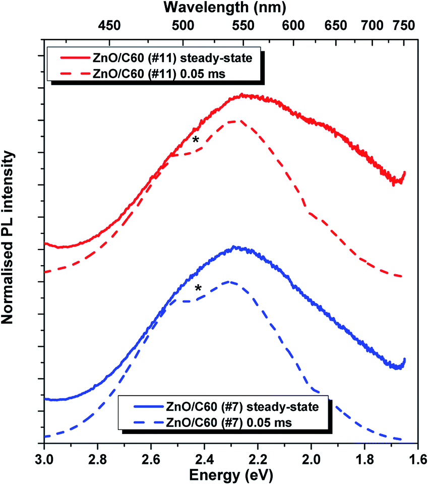 | ||
| Fig. 6 Normalised time-resolved (acquired with 0.05 ms of delay after flash) and steady-state PL spectra for ZnO/C60(#7) and ZnO/C60(#11) samples. The small signal depression denoted with an asterisk in the TRPL spectra corresponds to the blaze of the detection grating. | ||
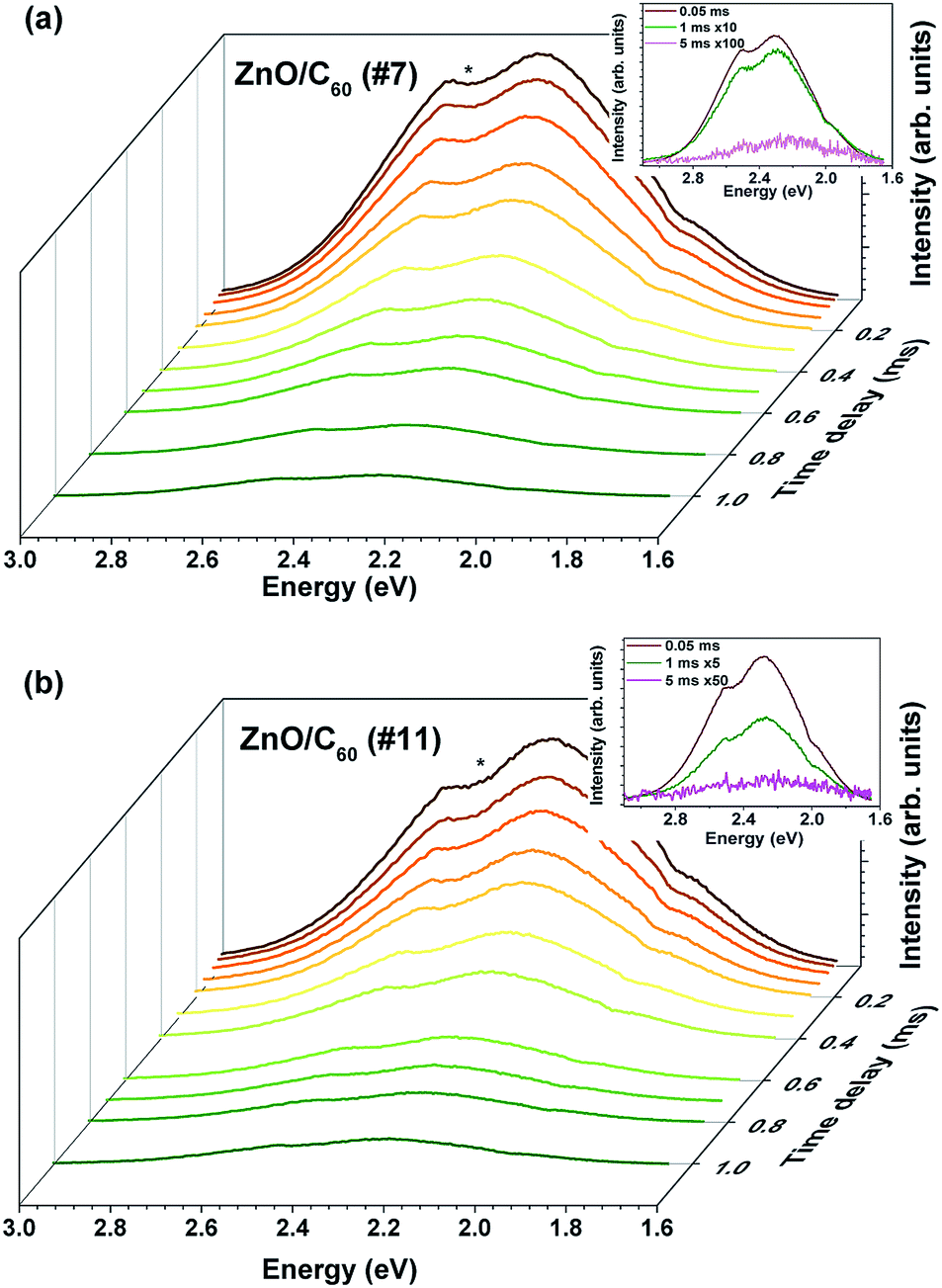 | ||
| Fig. 7 RT TRPL spectra monitored for the (a) ZnO/C60(#7) and (b) ZnO/C60(#11) samples, obtained after a 325 nm pulsed excitation for increasing delay times (with a time window of 10 ms). The small signal depression denoted by an asterisk corresponds to the blaze of the detection grating. The insets correspond to a comparison of the TRPL spectra for different time delays: 0.05, 1 and 5 ms. | ||
In order to get a deeper insight into the mechanisms involved in the different luminescence processes, the samples were cooled down to 11 K. Fig. 8 depicts the PL spectra acquired at low temperature for each sample. For all the cases, besides the visible emission, a well-resolved NBE recombination was measured allowing us to identify the free and donor-bound exciton recombinations, as well as the emission peaked at 3.31 eV and its phonon replicas. At this temperature, it was possible to identify the NBE emission for the reference sample, even though with an intensity two orders of magnitude lower than the visible broad band. For the samples coated with C60, the NBE is the dominant recombination of the overall luminescence spectra. Previous studies from our group, carried out also on ZnO rods grown by laser-assisted flow deposition (LAFD),26 revealed that the 3.31 eV emission is associated with the presence of surface states, as identified by the influence of distinct plasma treatments on the recombination intensity. This emission, also identified in C60 coated ZnO tetrapods,8 exhibits a relative intensity that increases with the increase of the C60 amount deposited on the ZnO surface. Such behaviour can be associated with a higher concentration of electron–hole pairs in the composites, surface when increasing the C60 content, leading to an increase in the excitonic and surface related transitions, corroborating previous studies on other ZnO/carbon composites8,64 and indicating charge transfer from C60 to the semiconductor surface, as mentioned previously.
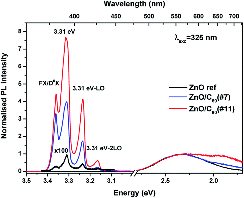 | ||
| Fig. 8 Low temperature (11 K) PL spectra of the ZnO, ZnO/C60(#7) and ZnO/C60(#11) samples. The PL spectra were obtained with the 325 nm He–Cd laser line and normalised to the broad emission maxima. The intensity of the NBE emission of the reference sample was multiplied by 100 in order to compare its features with the remaining samples. | ||
The effect of the excitation density on the UV emission was further studied for both samples coated with C60, as displayed in Fig. 9. The relative intensity of the spectra shows a strong dependence on the excitation power, as already observed for the ZnO rods produced by LAFD.26 In this case, as high resolution spectra were acquired, it is possible to clearly identify the presence of FX transitions. The relative intensity of the emission related to the exciton transitions increases in comparison with the 3.31 eV emission when the excitation density decreases. Similar behaviour was attributed by Schneider et al.65 to the saturation of the D0X recombination with increasing excitation density. As reported for the LAFD samples,26 the observed dependence of the relative intensity of the 3.31 eV vs. FX + D0X transitions as a function of the excitation density suggests a saturation effect of the exciton recombination with increasing power, leading to the change in the relative intensity of both lines.
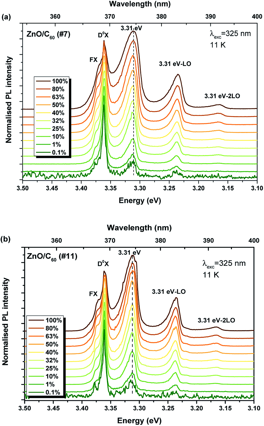 | ||
| Fig. 9 NBE excitation density dependent PL spectra of (a)ZnO/C60(#7) and (b) ZnO/C60(#11) samples. | ||
Fig. 10a shows the normalised PL spectra of the broad emission bands at 11 K (full lines) and RT (dash lines). As seen in the spectra, the peak position and spectral shape of the deep luminescence barely change with increasing temperature, with the main maximum likely dependent on the relative intensity of the defect centres that contribute to the observed emission bands. Temperature-dependent PL studies of the NBE recombination were also conducted for the sample with the highest PL intensity, ZnO/C60(#11), as shown in Fig. 10b. As expected, an increase in the temperature promotes the dissociation of the bound excitons and causes the decrease in the intensity of the D0X transitions due to nonradiative relaxation, accompanied by a red shift of the FX, 3.31 eV line emission and its replicas, following the bandgap shrinkage. Therefore, these results corroborate our previous assignments for the peaks observed at ∼3.26 eV and ∼3.2 eV.
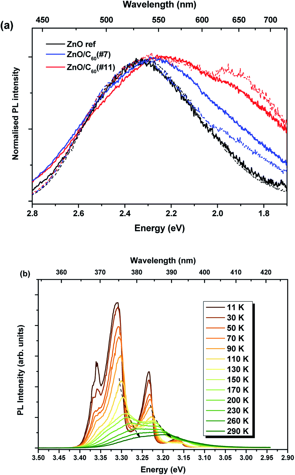 | ||
| Fig. 10 (a) 11 K (full lines) and RT (dash lines) PL spectra of the ZnO, ZnO/C60(#7) and ZnO/C60(#11) samples, obtained with the 325 nm He–Cd laser line and normalised to the broad emission maxima. (b) Temperature-dependent PL spectra of the NBE emission for the ZnO/C60(#11) sample. | ||
4. Conclusions
ZnO microwires synthesised by the flame transport technique coated with different C60 flooding amounts were investigated in detail by optical techniques. The comparison with the ZnO reference sample evidences that the formed ZnO/C60 composites promote the narrowing of the band tail states, accompanied by steeper bandgap absorption. Such behaviour indicates that, in the presence of C60, some of the carriers previously trapped at the band tail ZnO levels are now available to recombine from the semiconductor's energy bands, as identified by the increase in the intensity of the NBE recombination. Moreover, the increase in the intensity of the 3.31 eV emission indicates that carriers are also transferred from C60 to the semiconductor surface states. The here reported results suggest that the formation of ZnO/C60 composites with different C60 flooding amounts allows us to tune the number of charge carriers in ZnO. Indeed, the relative intensity of the excitonic and surface related ultraviolet recombination increases with the increase of deposited C60 flooding on the ZnO surface. Moreover, it was observed that the broad visible band was in fact composed by two optical components, one peaked in the green and another in the orange/red spectral regions. Excitation and time dependent results indicate a donor acceptor pair recombination nature for the two optical centres. Moreover, the intensity of the green emission drops by 1/e nearly after 1 ms, indicating lifetimes in the range of hundreds of μs. The orange/red emission band decays faster than the green one, which could not be detected with the used experimental set-up.Similarly to what was verified for the near band edge recombination, increasing the C60 flooding on the ZnO surface leads to an increase in the relative intensity of the orange/red component, which influences the peak position of the overall broad emission and its width. In particular, higher amounts of C60 result in a pronounced lower energy shift of the band maxima. Therefore, the optical response of the ZnO/C60 composites can be used to tailor the material light outcome and their surface-related properties may be handling for multifunctional approaches.
Conflicts of interest
There are no conflicts to declare.Acknowledgements
This work was financially supported by FEDER funds through the COMPETE 2020 Programme and National Funds through FCT - Portuguese Foundation for Science and Technology under projects UID/CTM/50025/2019 and POCI-01-0145-FEDER-028755. Kiel authors thank the Deutsche Forschungsgemeinschaft (DFG) for financial support under the scheme SFB 677 (C14). EN and BM thank Spanish MINECO for funding via the project MAT 2015-65274-R-FEDER.References
- S. S. Bhat, A. Qurashi and F. A. Khanday, TrAC, Trends Anal. Chem., 2017, 86, 1–13 CrossRef CAS.
- L. Zheng, Y. Wan, P. Qi, Y. Sun, D. Zhang and L. Yu, Talanta, 2017, 167, 600–606 CrossRef CAS PubMed.
- X. Dong, Y. Cao, J. Wang, M. B. Chan-Park, L. Wang, W. Huang and P. Chen, RSC Adv., 2012, 2, 4364 RSC.
- U. Özgür, Y. I. Alivov, C. Liu, A. Teke, M. A. Reshchikov, S. Doğan, V. Avrutin, S.-J. Cho and H. Morkoç, J. Appl. Phys., 2005, 98, 041301 CrossRef.
- Y. K. Mishra and R. Adelung, Mater. Today, 2017, 21, 631–651 CrossRef.
- O. Lupan, V. Postica, J. Gröttrup, A. K. Mishra, N. H. de Leeuw, J. F. C. Carreira, J. Rodrigues, N. Ben Sedrine, M. R. Correia, T. Monteiro, V. Cretu, I. Tiginyanu, D. Smazna, Y. K. Mishra and R. Adelung, ACS Appl. Mater. Interfaces, 2017, 9, 4084–4099 CrossRef CAS PubMed.
- V. Postica, J. Gröttrup, R. Adelung, O. Lupan, A. K. Mishra, N. H. de Leeuw, N. Ababii, J. F. C. Carreira, J. Rodrigues, N. Ben Sedrine, M. R. Correia, T. Monteiro, V. Sontea and Y. K. Mishra, Adv. Funct. Mater., 2017, 27, 1604676 CrossRef.
- D. Smazna, J. Rodrigues, S. Shree, V. Postica, G. Neubüser, A. F. Martins, N. Ben Sedrine, N. K. Jena, L. Siebert, F. Schütt, O. Lupan, R. Ahuja, M. R. P. Correia, T. Monteiro, L. Kienle, Y. Yang, Y. K. Mishra and R. Adelung, Nanoscale, 2018, 10, 10050–10062 RSC.
- H. Moussa, E. Girot, K. Mozet, H. Alem, G. Medjahdi and R. Schneider, Appl. Catal. B Environ., 2016, 185, 11–21 CrossRef CAS.
- N. A. Noor Azmy, A. A. A. Bakar, N. Arsad, S. Idris, A. R. Mohmad and A. Abdul Hamid, Appl. Surf. Sci., 2017, 392, 1134–1143 CrossRef CAS.
- Y. Zhao, W. Li, L. Pan, D. Zhai, Y. Wang and L. Li, Sci. Rep., 2016, 6, 32327 CrossRef CAS PubMed.
- K. Thonke, T. Gruber, N. Teofilov, R. Schönfelder, A. Waag and R. Sauer, Phys. B, 2001, 308, 945–948 CrossRef.
- H. Morkoç and Ü. Özgür, Zinc Oxide: Fundamentals, Materials and Device Technology, John Wiley & Sons, 2008 Search PubMed.
- Y. Park, C. Litton, T. Collins and D. Reynolds, Phys. Rev., 1966, 143, 512–519 CrossRef CAS.
- H. Priller, R. Hauschild, J. Zeller, C. Klingshirn, H. Kalt, R. Kling, F. Reuss, C. Kirchner and A. Waag, J. Lumin., 2005, 112, 173–176 CrossRef CAS.
- C. F. Klingshirn, B. K. Meyer, A. Waag, A. Hoffmann and J. M. M. Geurts, ZnO: From Fundamental Properties Towards Novel Applications, Springer, 2010 Search PubMed.
- R. Dingle, Phys. Rev. Lett., 1969, 23, 579–581 CrossRef CAS.
- A. B. Djurišić, Y. H. Leung, K. H. Tam, Y. F. Hsu, L. Ding, W. K. Ge, Y. C. Zhong, K. S. Wong, W. K. Chan, H. L. Tam, K. W. Cheah, W. M. Kwok and D. L. Phillips, Nanotechnology, 2007, 18, 095702 CrossRef.
- J. Rodrigues, A. J. Fernandes, T. Monteiro and F. Costa, CrystEngComm, 2019 10.1039/c8ce01773e.
- B. K. Meyer, H. Alves, D. M. Hofmann, W. Kriegseis, D. Forster, F. Bertram, J. Christen, A. Hoffmann, M. Straßburg, M. Dworzak, U. Haboeck and A. V. Rodina, Phys. Status Solidi, 2004, 241, 231–260 CrossRef CAS.
- K. Lischka, A. Waag, H. Mariette, J. Neugebauer, M. R. Wagner, H. W. Kunert, A. G. J. Machatine, A. Hoffmann, P. Niyongabo, J. Malherbe and J. Barnas, Microelectronics J., 2009, 40, 289–292 CrossRef.
- F. H. Leiter, H. R. Alves, A. Hofstaetter, D. M. Hofmann and B. K. Meyer, Phys. Status Solidi, 2001, 226, R4–R5 CrossRef CAS.
- N. Y. Garces, L. Wang, L. Bai, N. C. Giles, L. E. Halliburton and G. Cantwell, Appl. Phys. Lett., 2002, 81, 622 CrossRef CAS.
- A. B. Djurišić, Y. H. Leung, K. H. Tam, L. Ding, W. K. Ge, H. Y. Chen and S. Gwo, Appl. Phys. Lett., 2006, 88, 103107 CrossRef.
- D. Li, Y. H. Leung, A. B. Djurišić, Z. T. Liu, M. H. Xie, S. L. Shi, S. J. Xu and W. K. Chan, Appl. Phys. Lett., 2004, 85, 1601–1603 CrossRef CAS.
- J. Rodrigues, T. Holz, R. Fath Allah, D. Gonzalez, T. Ben, M. R. Correira, T. Monteiro and F. M. Costa, Sci. Rep., 2015, 5, 10783 CrossRef CAS PubMed.
- I. Shalish, H. Temkin and V. Narayanamurti, Phys. Rev. B: Condens. Matter Mater. Phys., 2004, 69, 245401 CrossRef.
- J. Fallert, R. Hauschild, F. Stelzl, A. Urban, M. Wissinger, H. Zhou, C. Klingshirn and H. Kalt, J. Appl. Phys., 2007, 101, 073506 CrossRef.
- N. S. N. And and D. R. Gamelin, J. Phys. Chem. B, 2005, 109, 20810–20816 CrossRef PubMed.
- Q. Wan, T. H. Wang and J. C. Zhao, Appl. Phys. Lett., 2005, 87, 083105 CrossRef.
- M. Y. Guo, A. M. C. Ng, F. Liu, A. B. Djurišić, W. K. Chan, H. Su and K. S. Wong, J. Phys. Chem. C, 2011, 115, 11095–11101 CrossRef CAS.
- A. Wei, L. Pan and W. Huang, Mater. Sci. Eng. B, 2011, 176, 1409–1421 CrossRef CAS.
- J. Rodrigues, A. Pimentel, E. Fortunato, T. Monteiro and F. M. Costa, Phys. Status Solidi, 2018, 1800155 CrossRef.
- F. Vietmeyer, B. Seger and P. V. Kamat, Adv. Mater., 2007, 19, 2935–2940 CrossRef CAS.
- M.-K. Lee, T. G. Kim, W. Kim and Y.-M. Sung, J. Phys. Chem. C, 2008, 112, 10079–10082 CrossRef CAS.
- X. Jin, M. Götz, S. Wille, Y. K. Mishra, R. Adelung and C. Zollfrank, Adv. Mater., 2013, 25, 1342–1347 CrossRef CAS PubMed.
- C.-T. Chen, F.-C. Hsu, S.-W. Kuan and Y.-F. Chen, Sol. Energy Mater. Sol. Cells, 2011, 95, 740–744 CrossRef CAS.
- E. A. Zakhidov, M. A. Zakhidova, A. M. Kokhkharov, S. K. Nematov, R. A. Nusretov and V. O. Kuvondikov, Appl. Sol. Energy, 2017, 53, 291–296 CrossRef.
- G. Hyun, S. Park, J. Jeong, K. S. Lee, D. I. Son, H. Lee and Y. Yi, J. Phys. Chem. C, 2017, 121, 12230–12235 CrossRef CAS.
- H. Fu, T. Xu, S. Zhu and Y. Zhu, Environ. Sci. Technol., 2008, 42, 8064–8069 CrossRef CAS PubMed.
- A. Vantomme, S. Hogg, M. Wu, B. Pipeleers, M. Swart, S. Goodman, D. Auret, K. Iakoubovskii, G. Adriaenssens, K. Jacobs and I. Moerman, Nucl. Instrum. Methods Phys. Res. Sect. B Beam Interact. Mater. Atoms, 2001, 175–177, 148–153 CrossRef CAS.
- P. Schulz, L. L. Kelly, P. Winget, H. Li, H. Kim, P. F. Ndione, A. K. Sigdel, J. J. Berry, S. Graham, J.-L. Brédas, A. Kahn and O. L. A. Monti, Adv. Funct. Mater., 2014, 24, 7381–7389 CrossRef CAS.
- S. K. Hong, J. H. Lee and W. B. Ko, J. Nanosci. Nanotechnol., 2011, 11, 6049–6056 CrossRef CAS PubMed.
- Y. K. Mishra, S. Kaps, A. Schuchardt, I. Paulowicz, X. Jin, D. Gedamu, S. Freitag, M. Claus, S. Wille, A. Kovalev, S. N. Gorb and R. Adelung, Part. Part. Syst. Char., 2013, 30, 775–783 CrossRef CAS.
- N. Faraji, C. Ulrich, N. Wolff, L. Kienle, R. Adelung, Y. K. Mishra and J. Seidel, Adv. Electron. Mater., 2016, 2, 1600138 CrossRef.
- F. Schütt, S. Signetti, H. Krüger, S. Röder, D. Smazna, S. Kaps, S. N. Gorb, Y. K. Mishra, N. M. Pugno and R. Adelung, Nat. Commun., 2017, 8, 1215 CrossRef PubMed.
- D. Smazna, N. Wolff, S. Shree, F. Schütt, Y. K. Mishra, L. Kienle and R. Adelung, in 2017 IEEE 7th International Conference Nanomaterials: Application & Properties (NAP), IEEE, 2017, p. 01FNC07 Search PubMed.
- T. Reimer, I. Paulowicz, R. Röder, S. Kaps, O. Lupan, S. Chemnitz, W. Benecke, C. Ronning, R. Adelung and Y. K. Mishra, ACS Appl. Mater. Interfaces, 2014, 6, 7806–7815 CrossRef CAS PubMed.
- O. Lupan, L. Chow, L. K. Ono, B. R. Cuenya, G. Chai, H. Khallaf, S. Park and A. Schulte, J. Phys. Chem. C, 2010, 114, 12401–12408 CrossRef CAS.
- Y. K. Mishra, G. Modi, V. Cretu, V. Postica, O. Lupan, T. Reimer, I. Paulowicz, V. Hrkac, W. Benecke, L. Kienle and R. Adelung, ACS Appl. Mater. Interfaces, 2015, 7, 14303–14316 CrossRef CAS PubMed.
- R. Cuscó, E. Alarcón-Lladó, J. Ibáñez, L. Artús, J. Jiménez, B. Wang and M. Callahan, Phys. Rev. B: Condens. Matter Mater. Phys., 2007, 75, 165202 CrossRef.
- J. Rodrigues, A. J. S. Fernandes, D. Mata, T. Holz, R. G. Carvalho, R. Fath Allah, T. Ben, D. Gonzalez, R. F. Silva, A. F. da Cunha, M. R. Correia, L. C. Alves, K. Lorenz, A. J. Neves, F. M. Costa and T. Monteiro, in SPIE OPTO, ed. F. H. Teherani, D. C. Look and D. J. Rogers, International Society for Optics and Photonics, 2014, p. 89871F Search PubMed.
- S. Guha, J. Menéndez, J. B. Page, G. B. Adams, G. S. Spencer, J. P. Lehman, P. Giannozzi and S. Baroni, Phys. Rev. Lett., 1994, 72, 3359–3362 CrossRef CAS PubMed.
- C. Jagadish and S. J. Pearton, Zinc oxide bulk, thin films and nanostructures: processing, properties and applications, Elsevier, 2006 Search PubMed.
- H. Zeng, G. Duan, Y. Li, S. Yang, X. Xu and W. Cai, Adv. Funct. Mater., 2010, 20, 561–572 CrossRef CAS.
- A. F. Kohan, G. Ceder, D. Morgan and C. G. Van De Walle, Phys. Rev. B: Condens. Matter Mater. Phys., 2000, 61, 19–27 CrossRef.
- A. B. Djurišić, W. C. H. Choy, V. A. L. Roy, Y. H. Leung, C. Y. Kwong, K. W. Cheah, T. K. GunduRao, W. K. Chan, H. FeiLui and C. Surya, Adv. Funct. Mater., 2004, 14, 856–864 CrossRef.
- M. Baibarac, I. Baltog, A. Matea and S. Lefrant, J. Cryst. Growth, 2015, 419, 158–164 CrossRef CAS.
- J. Rodrigues, D. Mata, A. J. S. Fernandes, M. A. Neto, R. F. Silva, T. Monteiro and F. M. Costa, Acta Mater., 2012, 60, 5143–5150 CrossRef CAS.
- Y. Hu and H.-J. Chen, Mater. Res. Bull., 2008, 43, 2153–2159 CrossRef CAS.
- T. Frade, D. Siopa, A. F. Martins, J. F. C. Carreira, J. Rodrigues, N. Ben Sedrine, M. R. Correia, T. Monteiro, R. Tena-Zaera and A. Gomes, J. Electrochem. Soc., 2018, 165, D595–D603 CrossRef CAS.
- P. Y. Yu and M. Cardona, Fundamentals of Semiconductors: Physics And Materials Properties, Springer, 2005, vol. 3 Search PubMed.
- J. I. Pankove, Optical Processes in Semiconductors, Dover Publication, Inc., 1971 Search PubMed.
- J. Rodrigues, D. Mata, A. Pimentel, D. Nunes, R. Martins, E. Fortunato, A. J. Neves, T. Monteiro and F. M. Costa, Mater. Sci. Eng. B, 2015, 195, 38–44 CrossRef CAS.
- M. Schirra, R. Schneider, A. Reiser, G. M. Prinz, M. Feneberg, J. Biskupek, U. Kaiser, C. E. Krill, K. Thonke and R. Sauer, Phys. Rev. B: Condens. Matter Mater. Phys., 2008, 77, 125215 CrossRef.
| This journal is © The Royal Society of Chemistry 2019 |