
 Open Access Article
 This Open Access Article is licensed under a Creative Commons Attribution-Non Commercial 3.0 Unported Licence
Growth of graphene with large single-crystal domains by Ni foam-assisted structure and its high-gain field-effect transistors†
Xuedong
Gao
 ,
Cui
Yu
*,
Zezhao
He
,
Xubo
Song
,
Qingbin
Liu
,
Chuangjie
Zhou
,
Jianchao
Guo
,
Shujun
Cai
and
Zhihong
Feng
*
,
Cui
Yu
*,
Zezhao
He
,
Xubo
Song
,
Qingbin
Liu
,
Chuangjie
Zhou
,
Jianchao
Guo
,
Shujun
Cai
and
Zhihong
Feng
*
National Key Laboratory of Application Specific Integrated Circuit, Hebei Semiconductor Research Institute, Shijiazhuang 050051, Hebei Province, China. E-mail: yucui1@163.com; ga917vv@163.com; Tel: +86-311-8709-1835
First published on 13th December 2018
Abstract
High-quality graphene materials and high-performance graphene transistors have attracted much attention in recent years. To obtain high-performance graphene transistors, large single-crystal graphene is needed. The synthesis of large-domain-sized single-crystal graphene requires low nucleation density; this can lead to a lower growth rate. In this study, a Ni-foam assisted structure was developed to control the nucleation density and growth rate of graphene by tuning the flow dynamics. Lower nucleation density and high growth rate (∼50 μm min−1) were achieved with a 4 mm-gap Ni foam. With the graphene transistor fabrication process, a pre-deposited Au film as the protective layer was used during the graphene transfer. Graphene transistors showed good current saturation with drain differential conductance as low as 0.04 S mm−1 in the strong saturation region. For the devices with gate length of 2 μm, the intrinsic cut-off frequency fT and maximum oscillation frequency fmax were 8.4 and 16.3 GHz, respectively, with fmax/fT = 1.9 and power gain of up to 6.4 dB at 1 GHz. The electron velocity saturation induced by the surface optical phonons of SiO2 substrates was analyzed. Electron velocity saturation and ultra-thin Al2O3 gate dielectrics were thought to be the reasons for the good current saturation and high power gain of the graphene transistors.
Introduction
Graphene as the two-dimensional structure of graphite exhibits numerous extraordinary physical, chemical, optical, biological and electronic properties.1,2 The high carrier mobility of graphene results in its promising application in high-speed field-effect transistors (FETs). The performance of graphene FETs depends on the quality of the graphene channel. In this aspect of graphene growth, a larger single-crystal domain indicates reduced boundary in the graphene channel, and it tends to maintain high electronic characteristics in graphene FETs.3 Therefore, the growth of large single-crystal graphene is imperative. Low cost and large area are obtained using the Cu-catalysed chemical vapor deposition (CVD) method, which is a promising approach to achieve large single-crystal graphene growth.4The key to the growth of larger single-crystal graphene is to maintain low nucleation density in the CVD process.5 There are several approaches such as controlling the nucleation density on Cu foils, smoothening the surface of Cu foil, growth of Cu oxide, substantially reducing the CH4 percentage, and controlling the channel structure or tube shape.5–9 The above methods can effectively increase the size of single-crystal graphene. However, the low nucleation density also leads to a lower growth rate; most growth rates are in the range of 1–10 μm min−1, due to which a longer time is required for larger single-crystal graphene growth.5,9–12
For graphene transistors used in wireless communication circuits, high gain values still hinder the application due to lack of current saturation.13–16 The way to obtain current saturation is to open a bandgap by nanopatterning of monolayer graphene (MLG)17 or by applying vertical electric displacement on Bernal-stacked bilayer graphene (BLG).18,19 These methods have their respective drawbacks for practical application. Thinning the gate dielectric is thought to be another efficient way to obtain current saturation.20
In this study, we design a simple Ni foam-assisted structure to control the graphene growth on a Cu foil. With the Ni foam, the nucleation density and growth kinetics of graphene are controlled. The state of the precursors on the top surface of the Cu foil is controlled by regulating the gap of the Ni foam and Cu foil. With the Ni foam-assisted graphene growth, the nucleation density is lowered to 1/mm2, and the growth rate can be higher than 50 μm min−1. A Au film was pre-deposited on the graphene surface as a protective layer to avoid the contamination of graphene during the transfer and FET fabrication process. By thinning the gate dielectric Al2O3 down to 5 nm, graphene FETs with gate length of 2 μm show good current saturation and power gain up to 6.4 dB at 1 GHz.
Experimental
Growth and characterization of graphene
Cu foil (98%, 25 μm, Alfa Aesar) was oxidized at 200 °C for 20 min on a hot plate. The growth of graphene was conducted in a vertical-type chemical vapor deposition furnace. The Cu foil was loaded onto the heater, and the pressure was controlled at 25 mbar. Ar gas with a flow of 1000 sccm was used to remove the air, and the temperature was kept at 1000 °C for 10 min. Then, graphene was grown at 1000 °C with a methane flow of 2 sccm and H2 flow of 60 sccm. The size and nucleation density of graphene were measured by optical microscopy (OM). The Cu foil with graphene was oxidized at 160 °C for 10 min on a hot plate to increase the contrast for OM observation. Micro-Raman scattering experiments were performed at RT with a spectrometer (514 nm).Graphene transfer
After the growth of graphene on the Cu foil, 30 nm of Au film was immediately deposited onto the graphene surface on the top side of the Cu foil. The graphene on the bottom side of Cu foil was removed by O2 plasma. Cu foil was etched by FeCl3 aqueous solution and then, the Au/graphene film was rinsed in deionized water three times. Au/graphene was transferred onto an SiO2/Si wafer; the thickness of SiO2 was 90 nm. Au/graphene/SiO2/Si was dried at 90 °C for 20 min.Device fabrication
Graphene FETs were fabricated by a self-aligned process following the method reported in our previous study.21 Optical lithography was adopted to define the channel regions, followed by electrical isolation by exposing the graphene surface to oxygen plasma after removal of the Au film outside the channel. We deposited Ti 20 nm/Pt 50 nm/Au 150 nm to form the electrode pads. Gates of 2 μm were patterned by optical lithography. Subsequently, the Au layer under the gates was wet-etched to form a self-aligned source and drain ohmic contacts automatically. Next, 1.7 nm-thick Al was deposited by e-beam evaporation, which was then oxidised in air for 1 day at room temperature to form an Al2O3 dielectric. The thickness of the alumina was tAl2O3 ≈ 5 nm. Finally, a 150 nm-thick Al metal film was evaporated to form the gate electrodes.Results and discussion
Ni foam is used to assist the graphene growth by controlling the precursor flow dynamics. Fig. 1(a) shows the schematic of Ni foam-assisted graphene growth. The distance between the Ni foam and Cu substrate is 4 mm. The flow rate of the precursors decreases due to the Ni foam on the top of the Cu substrate; the decreased flow rate can lead to lower nucleation density and a higher growth rate, as shown in Fig. 1(c), with a growth time of 15 min. The schematic without Ni foam-assisted graphene growth is shown in Fig. 1(b). Fig. 1(d) shows the results without Ni foam-assisted growth. The growth time is 10 min. Fig. 1(d) shows very high nucleation density and slower growth rate compared with Fig. 1(c), demonstrating that we can decrease the nucleation density and increase the growth rate with the Ni foam-assisted graphene growth process.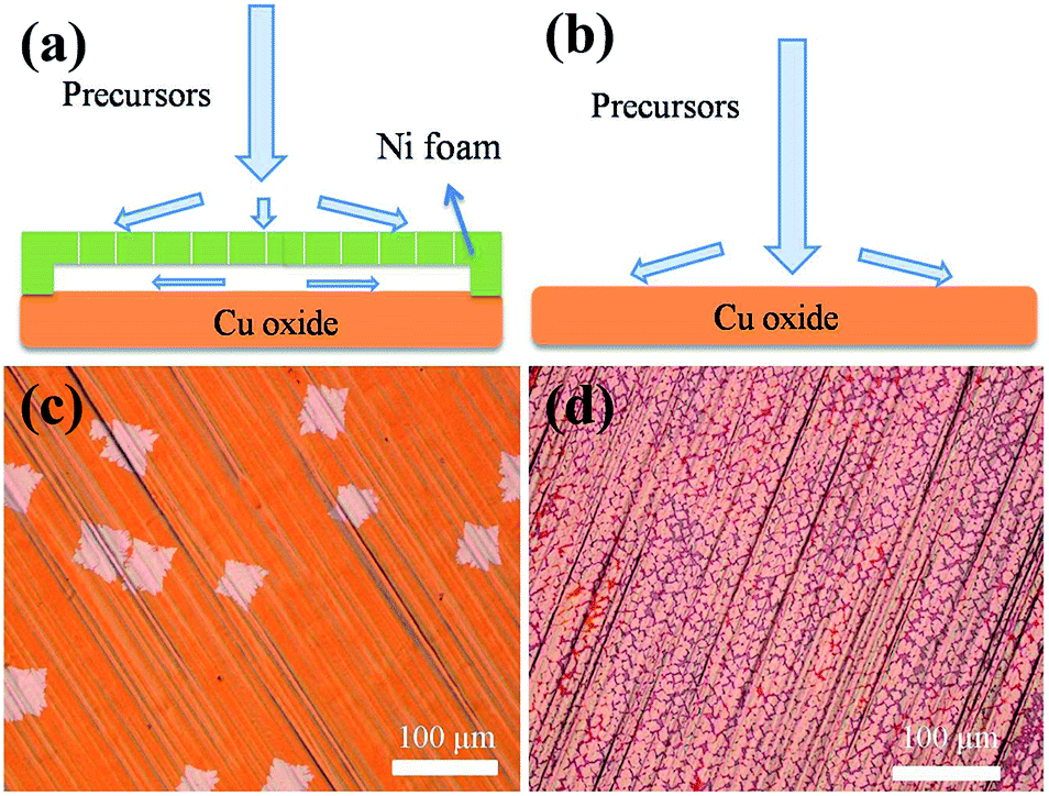 | ||
| Fig. 1 (a) Schematic image and (c) OM image of Ni foam-assisted graphene growth with a growth time of 15 min; (b) schematic image and (d) OM image of conventional graphene growth on Cu foil with a growth time of 10 min. | ||
The mechanism of the influence of Ni foam in the graphene growth process was studied. The Cu foil was oxidized before insertion into the tube, and we used EDX to study the oxygen coverage on the Cu foil. SEM and EDX images are shown in Fig. S1.† After heating to 1030 °C under Ar gas for 10 min, the oxygen coverage of the Cu foil surface with the Ni foam structure was significantly higher than that without the Ni foam-assisted structure. With the Ni foam structure, the surface oxygen coverage was at 4.62%, and without the Ni foam structure, the surface oxygen coverage was at 1.28%. The higher oxygen content can suppress the nucleation and improve the graphene growth rate.22
To study the effect of the precursor flow rate, graphene growth under different gaps between the Ni foam and Cu substrate is studied. The gaps are set as 3 mm, 4 mm, and 5 mm. The growth times of graphene with and without Ni foam are 15 min and 10 min, respectively. Fig. 2(a), (b) and (c) show the graphene growth with 3 mm, 4 mm, and 5 mm gaps, respectively. It can be found that the nucleation density increases as the gap increases. Fig. 2(d) shows the graphene grown without Ni foam; the nucleation density is very high (∼1.2 × 10⁴/mm2) and the graphene size is very small. Fig. 2(e) shows the corresponding nucleation density of the Ni foam-assisted graphene growth with different gaps. As the Ni foam gap increases, the precursor flow rate increases, resulting in higher nucleation density. Fig. 2(f) shows the average growth rate of graphene with different gaps. The rate of graphene growth is the highest in the 4 mm Ni foam gap. Without Ni foam, the graphene growth has very high precursor flow rate but a lower growth rate. The above results show that 4 mm Ni foam gap is appropriate for assisted graphene growth; it can maintain a higher growth rate and a relatively lower nucleation density.
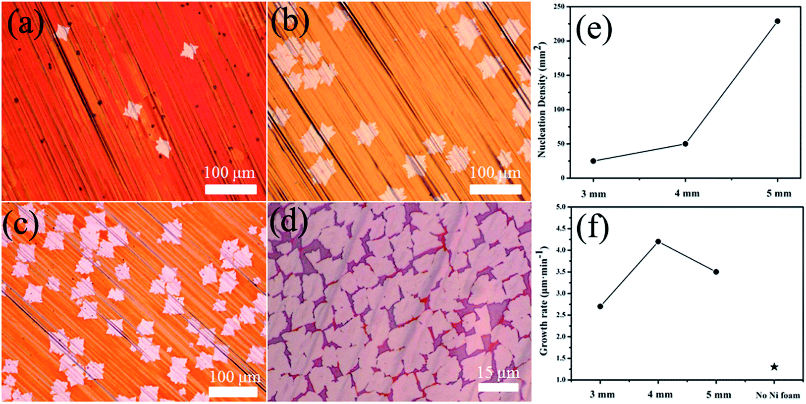 | ||
| Fig. 2 Graphene growth under different gaps between the Ni foam and Cu substrate. Gap size: (a) 3 mm, (b) 4 mm, and (c) 5 mm. (d) Graphene growth without the Ni foam. (e) Nucleation density. (f) Growth rate of graphene with different Ni foam gaps. | ||
Fig. 3 shows the images of graphene growth with Ni foam (4 mm gap) and without Ni foam at 1060 °C. For graphene with Ni foam grown at 1060 °C for 10 min, the grain size of graphene is about 512 μm, as shown in Fig. 3(a). The nucleation density is ∼1/mm2 and growth rate is ∼51.2 μm min−1. With prolonged growth time, the grain size of graphene reaches millimeter scale. Fig. 3(b) shows graphene grown for 1 min without Ni foam at 1060 °C. The nucleation density shows no decrease as the growth temperature increases to 1060 °C. Fig. 3(c) and (d) show the OM images of the transferred graphene onto SiO2/Si substrates. Fig. 3(c) shows the image of graphene growth with Ni foam. The surface of graphene in optical microscopy view is very clear. There are many adlayers for graphene grown without Ni foam, as shown in Fig. 3(d). This is mainly due to the large number of boundaries between the small grains. Precursors go through to the boundary, forming many adlayers. Fig. 3(e) and (f) show the Raman shift of transferred graphene on the SiO2/Si substrates. As shown in Fig. 3(e), for graphene grown with Ni foam, the intensity ratio of the 2D/G peak is 3.4 with no clear D peak, demonstrating a single-layer graphene of high-quality.23 For graphene grown without Ni foam, the Raman shifts of the single-layer and adlayers (in Fig. 3(d)) are given in Fig. 3(f). The intensity ratio of the 2D/G peak is 3.5 for the adlayer graphene, demonstrating that adlayers do not exhibit an AB stacking structure.24 The relative intensity of the D/G peak in Fig. 3(f) is higher than that in Fig. 3(e), demonstrating that the quality of graphene grown with Ni foam is higher than that without Ni foam.23
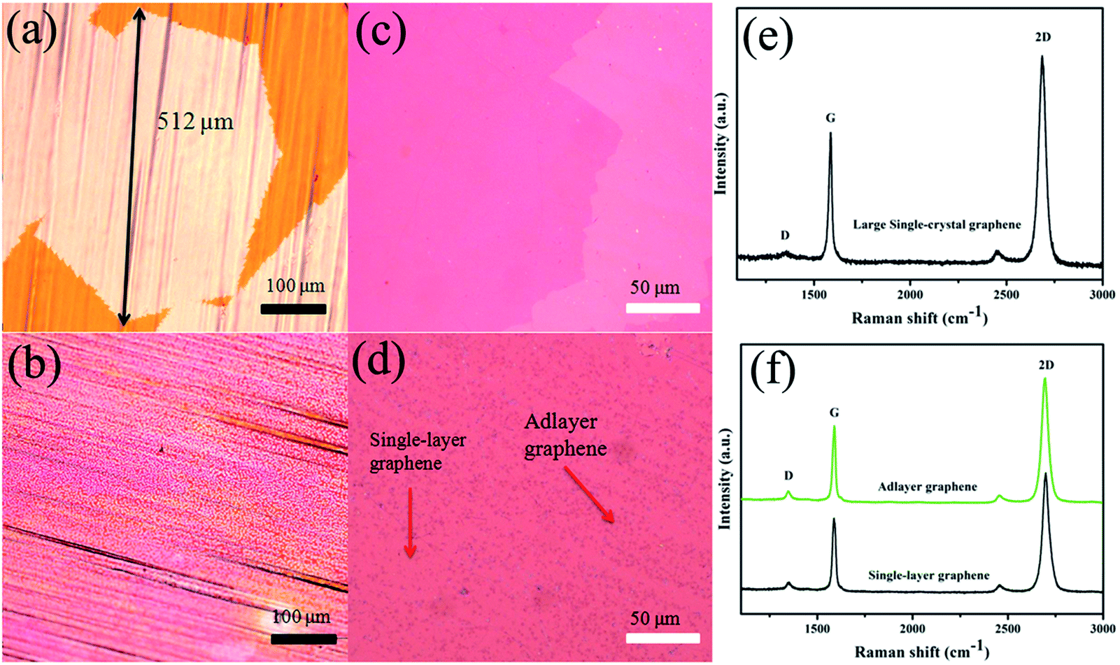 | ||
| Fig. 3 OM images of graphene growth on Cu foil (a) with Ni foam (4 mm gap) and (b) without Ni foam at 1060 °C. OM images and Raman pattern of graphene transferred to the SiO2/Si substrates: (c, e) with Ni foam (4 mm gap) and (d, f) without Ni foam. | ||
The relationship between the growth rate and material quality was studied. We set up five sets of experiments. The first experiment involved the fabrication of a Cu foil without a Ni foam-assisted structure with growth temperature of 1000 °C; the other experiments involved the fabrication of Cu foils with 4 mm-gap Ni foam with growth temperatures of 1000 °C, 1020 °C, 1040 °C and 1060 °C. The graphene growth rates in these five samples are found to be ∼1 μm min−1, ∼4 μm min−1, ∼12 μm min−1, ∼23 μm min−1 and ∼50 μm min−1. The Raman shifts of these five graphene samples were also studied. The Raman results are shown in Fig. S2.† The FWHM values of the 2D peaks of the five samples are 38 cm−1, 37 cm−1, 39 cm−1, 38 cm−1 and 43 cm−1, showing that the samples are all monolayer graphene. It was also found that the ID/IG ratios decrease as the growth rates increase. The ID/IG ratios of the five samples are 0.05, 0.03, 0.03, 0.02 and 0.02. The larger ID/IG ratio of the graphene sample with a growth rate of ∼1 μm min−1 may be mainly due to the small single-crystal size and numerous grain boundaries.
The fabrication schedule and OM image of graphene FETs fabricated by a self-aligned process are shown in Fig. S3.† Dual-gate graphene transistors with gate length of 2 μm and gate width of 100 μm × 2 were fabricated. The field-effect mobility values of the graphene transistors were 2450 cm2 V−1 s−1 (hole) and 3307 cm2 V−1 s−1 (electron), respectively (Fig. 4(d)), indicating the high quality of the graphene material and less contamination in the device fabrication process.
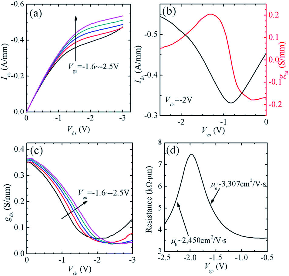 | ||
| Fig. 4 DC characteristics of the graphene transistors. (a) The current–voltage characteristics at gate voltages ranging from −1.6 V to −2.5 V. (b) Transfer characteristics at Vds = −2 V with −2.5 V ≤ Vgs ≤ 0 V. (c) Drain differential conductance gds. (d) Scaled resistance of a graphene transistor versus gate voltage at Vds = −0.1 V. | ||
Fig. 4 shows the DC electrical transport characteristics of graphene FETs. The DC electrical transport measurements were obtained using a Semiconductor Parameter Analyser (SPA). As shown in Fig. 4(a), the drain current (Ids) shows strong saturation with maximum scaled on-current Ids reaching 0.54 A mm−1. The sample shows n-type doping with the Dirac point at Vgs = −0.85 V and the maximum transconductance (gm) is measured at Vds = −2 V is 0.2 S mm−1, as shown in Fig. 4(b). Due to the strong drain current saturation, the drain differential conductance (gds) is small, as shown in Fig. 4(c). The gds value is as low as 0.04 S mm−1 in the strong saturation region (−2 V ≤ Vds ≤ −3 V).
High-frequency scattering parameters (S-parameters) of the transistors were measured up to 10 GHz using standard GSG probes. Fig. 5(a)–(c) show the as-measured, de-embedded, and intrinsic short-circuit current gain (|H21|2), maximum stable/available gain (MSG/MAG), and Mason's unilateral power gain (U) extracted from S-parameters for the graphene transistor with Lg = 2 μm and Wg = 100 μm × 2. As a result, the intrinsic cut-off frequency fT and maximum oscillation frequency fmax were determined to be 8.4 and 16.3 GHz for the device. The calculated fmax values from the maximum stable/available gain (MSG/MAG) and Mason's unilateral power gain (U) showed good consistency with each other, indicating the veracity of the derivation process.
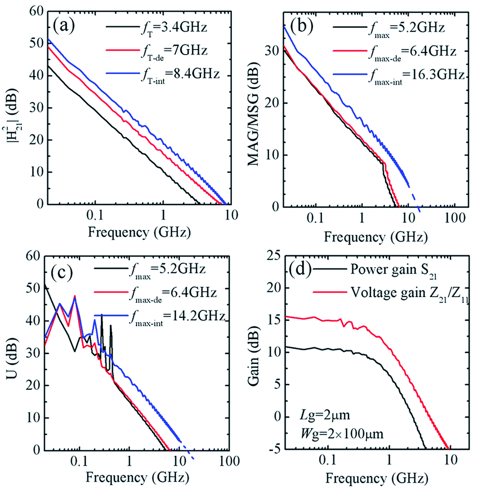 | ||
| Fig. 5 High-frequency characteristics of the GFET with a gate length of 2 μm and a gate width of 100 μm × 2. (a) Measured, de-embedded, and intrinsic |H21|2; (b) measured, de-embedded, and intrinsic maximum stable/available gain (MSG/MAG); (c) measured, de-embedded, and intrinsic Mason's unilateral power gain (U); and (d) measured frequency response of AC open-circuit voltage gain (Z21/Z11) and forward power gain (|S21|). | ||
Fig. 5(d) shows forward power gain |S21| and the AC open-circuit voltage gain Z21/Z11 as a function of frequency for the graphene transistor. The AC open-circuit voltage gain reaches 15 dB for the measured frequency range. Power gain |S21|, which reflects the real power amplification of a two-port network, is around 6.4 dB at 1 GHz for the device, which is among the highest reported values for CVD graphene transistors.25,26 The graphene FETs show very high power gain, which is a result of the strong drain current saturation-induced low drain differential conductance (gds).
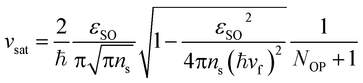
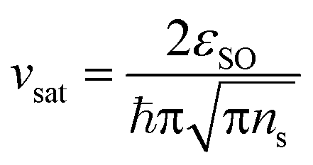
There are two possible reasons for the strong drain current saturation. One is the electron velocity saturation induced by the surface optical phonons of SiO2 substrates.27,28 In the case of graphene with mobility limited by impurity scattering, the high field behavior is determined by the emission of surface optical phonons in the SiO2 substrate.29 The energy of the surface optical phonons of SiO2 is εSO ≈ 59 meV. From εSO, the saturated electron velocity vsat can be estimated via emission of the surface optical phonons, which is denoted as follows:30,31
 | (1) |
 | (2) |
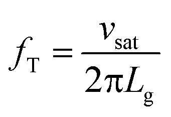
Table 1 shows the small signal model parameters of GFET.32–34 The extracted gate capacitance Cg = Cgs + Cgd is 1748 fF. The sheet density of the graphene channel can be estimated by ns = VDirac × Cg/e.35 The sample shows n-type doping with the Dirac point at Vgs = −0.85 V, and the calculated graphene channel (ns) is 2.3 × 1012 cm−2. From eqn (2), one can expect saturated electron velocity of 1.5 × 107 cm s−1 with ns = 2.3 × 10¹²/cm−2 in the graphene on Si/SiO2 substrates. The intrinsic cut-off frequency fT in an FET can be estimated as follows:
| C gd (fF) | C gs (fF) | C ds (fF) | g ds (mS) | g m (mS) | R i (Ω) | R g (Ω) | R s (Ω) | R d (Ω) |
|---|---|---|---|---|---|---|---|---|
| 341 | 1407 | 785 | 17 | 96 | 3.2 | 5 | 6.5 | 6.5 |
For a graphene transistor with gate length Lg of 2 μm, the estimated intrinsic cut-off frequency fT is 12 GHz for nsh of 2.3 × 1012 cm−2. The measured intrinsic fT of our device is 8.4 GHz, which is slightly lower than the estimated one, indicating that the electron velocity can achieve saturation. The ultra-thin self-oxidized AlOx gate dielectric should also be helpful in drain current saturation. Han et al. have shown that the low-density state (DOS) of graphene can help obtain drain current saturated characteristics in thin dielectric devices.20 They demonstrated that by employing a very thin gate dielectric (equivalent oxide thickness (EOT) less than 2 nm), full drain current saturation can be obtained for graphene FETs with short channels. EOT of graphene FETs in this study is approximately 2 nm, which will be beneficial for current saturation.
Conclusions
With a Ni foam-assisted structure to control the graphene growth on a Cu foil, graphene with grain size of millimeters was prepared. A pre-deposited Au film as a protective layer to avoid the pollution of graphene was used during the transfer and graphene FET fabrication process. Graphene FETs with gate length of 2 μm show good current saturation and power gain up to 6.4 dB at 1 GHz. Electron velocity saturation induced by surface optical phonons of SiO2 substrates and ultra-thin gate dielectric were thought to be the reasons for good current saturation and high power gain. Graphene transistors with short gate length will be developed in the next study to push frequency and power gain.Conflicts of interest
There are no conflicts to declare.Acknowledgements
This work was supported by the National Natural Science Foundation of China (61674131 and 61306006) and Basic Research Program of Hebei (18961020D).Notes and references
- Z. Guoke, X. Li, M. Huang, Z. Zhen, Y. Zhong, Q. Chen, X. Zhao, Y. He, R. Hu and T. Yang, et al. The Physics and Chemistry of Graphene-on-Surfaces, Chem. Soc. Rev., 2017, 46, 4417–4449 RSC.
- A. H. Castro Neto, N. M. R. Peres, K. S. Novoselov and A. K. Geim, The physics of heavy Z′ gauge bosons, Rev. Mod. Phys., 2009, 81, 1199–1228 CrossRef.
- Z. Hailong, W. Jong Yu, L. Liu, R. Cheng, Y. Chen, X. Huang, Y. Liu, Y. Wang, Y. Huang and X. Duan, Chemical Vapour Deposition Growth of Large Single Crystals of Monolayer and Bilayer Graphene, Nat. Commun., 2013, 4, 2096 CrossRef PubMed.
- W. Huan, X. Xu, J. Li, L. Lin, L. Sun, X. Sun, S. Zhao, C. Tan, C. Chen and W. Dang, et al. Surface Monocrystallization of Copper Foil for Fast Growth of Large Single-Crystal Graphene under Free Molecular Flow, Adv. Mater., 2016, 28, 8968–8974 CrossRef.
- C. Ren-Jie, C.-H. Lee, M.-K. Lee, C.-W. Chen and C.-Y. Wen, Effects of Surface Oxidation of Cu Substrates on the Growth Kinetics of Graphene by Chemical Vapor Deposition, Nanoscale, 2017, 9, 2324–2329 RSC.
- Y. Zheng, J. Lin, Z. Peng, Z. Sun, Y. Zhu, L. Li, C. Xiang, E. Loic Samuel, C. Kittrell and J. M. Tour, Toward the Synthesis of Wafer-Scale Single-Crystal Graphene on Copper Foils, ACS Nano, 2012, 6, 9110–9117 CrossRef.
- W. Ruizhe, J. Pan, X. Ou, Q. Zhang, Y. Ding, P. Sheng and Z. Luo, Concurrent Fast Growth of Sub-Centimeter Single-Crystal Graphene with Controlled Nucleation Density in a Confined Channel, Nanoscale, 2017, 9, 9631–9640 RSC.
- L. Xuesong, C. W. Magnuson, A. Venugopal, R. M. Tromp, J. B. Hannon, E. M. Vogel, L. Colombo and R. S. Ruoff, Large-Area Graphene Single Crystals Grown by Low-Pressure Chemical Vapor Deposition of Methane on Copper, J. Am. Chem. Soc., 2011, 133, 2816–2819 CrossRef.
- C. Shanshan, H. Ji, H. Chou, Q. Li, H. Li, J. Won Suk, R. Piner, L. Liao, W. Cai and R. S. Ruoff, Millimeter-Size Single-Crystal Graphene by Suppressing Evaporative Loss of Cu During Low Pressure Chemical Vapor Deposition, Adv. Mater., 2013, 25, 2062–2065 CrossRef.
- L. Xuesong, W. Cai, J. An, S. Kim, J. Nah, D. Yang, R. Piner, A. Velamakanni, I. Jung and E. Tutuc, et al. Large-Area Synthesis of High-Quality and Uniform Graphene Films on Copper Foils, Science, 2009, 324, 1312–1314 CrossRef PubMed.
- J. Li, X. Y. Wang, X. R. Liu, Z. Jin, D. Wang and L. J. Wan, Facile growth of centimeter-sized single-crystal graphene on copper foil at atmospheric pressure, J. Mater. Chem. C, 2015, 3, 3530–3535 RSC.
- H. Yufeng, M. S. Bharathi, L. Wang, Y. Liu, H. Chen, S. Nie, X. Wang, H. Chou, C. Tan and B. Fallahazad, et al. The Role of Surface Oxygen in the Growth of Large Single-Crystal Graphene on Copper, Science, 2013, 342, 720–723 CrossRef PubMed.
- L. Liao, J. Bai, R. Cheng, H. Zhou, L. Liu, Y. Liu, Y. Huang and X. F. Duan, Scalable Fabrication of Self-Aligned Graphene Transistors and Circuits on Glass, Nano Lett., 2012, 12, 2653–2657 CrossRef CAS.
- Y. Wu, K. A. Jenkins, A. Valdes-Garcia, D. B. Farmer, Y. Zhu, A. A. Bol, C. Dimitrakopoulos, W. Zhu, F. Xia, P. Avouris and Y. M. Lin, State-of-the-Art Graphene High-Frequency Electronics, Nano Lett., 2012, 12, 3062–3067 CrossRef CAS PubMed.
- S. Vaziri, A. D. Smith, M. Ostling, G. Lupina, J. Dabrowski, G. Lippert, W. Mehr, F. Driussi, S. Venica and V. Di Lecce, et al. Going Ballistic: Graphene Hot Electron Transistors, Solid State Commun., 2015, 224, 64–75 CrossRef CAS.
- G. Filippo, G. Greco, F. Roccaforte and S. Sonde, Vertical Transistors Based on 2D Materials: Status and Prospects, Crystals, 2018, 8(2), 70 CrossRef.
- X. Li, X. Wang, L. Zhang, S. Lee and H. Dai, Chemically derived, ultrasmooth graphene nanoribbon semiconductors, Science, 2008, 319, 1229–1232 CrossRef CAS PubMed.
- T. Ohta, A. Bostwick, T. Seyller, K. Horn and E. Rotenberg, Controlling the electronic structure of bilayer graphene, Science, 2006, 313, 951–954 CrossRef CAS PubMed.
- B. N. Szafranek, G. Fiori, D. Schall, D. Neumaier and H. Kurz, Current Saturation and Voltage Gain in Bilayer Graphene Field Effect Transistors, Nano Lett., 2012, 12, 1324–1328 CrossRef CAS.
- S. J. Han, D. Reddy, G. D. Carpenter, A. D. Franklin and K. A. Jenkins, Current Saturation in Submicrometer Graphene Transistors with Thin Gate Dielectric: Experiment, Simulation, and Theory, ACS Nano, 2012, 6, 5220–5226 CrossRef CAS.
- Z. H. Feng, C. Yu, J. Li, Q. B. Liu, Z. Z. He, X. B. Song, J. J. Wang and S. J. Cai, An Ultra Clean Self-Aligned Process for High Maximum Oscillation Frequency Graphene Transistors, Carbon, 2014, 75, 249–254 CrossRef CAS.
- Z. Zhihong, X. Xu, L. Qiu, S. Wang, T. Wu, F. Ding, H. Peng and K. Liu, The Way towards Ultrafast Growth of Single-Crystal Graphene on Copper, Adv. Sci., 2017, 4(9), 1700087 CrossRef PubMed.
- A. C. Ferrari, Raman spectroscopy of graphene and graphite: Disorder, electron–phonon coupling, doping and nonadiabatic effects, Solid State Commun., 2007, 143, 47–57 CrossRef CAS.
- Z. H. Ni, H. M. Wang, J. Kasim, H. M. Fan, T. Yu, Y. H. Wu, Y. P. Feng and Z. X. Shen, Graphene Thickness Determination Using Reflection and Contrast Spectroscopy, Nano Lett., 2007, 9, 2758–2763 CrossRef PubMed.
- M. Tian, X. Li, T. Li, Q. Gao, X. Xiong, Q. Hu, M. Wang, X. Wang and Y. Wu, High-Performance CVD Bernal-Stacked Bilayer Graphene Transistors for Amplifying and Mixing Signals at High Frequencies, ACS Appl. Mater. Interfaces, 2018, 10, 20219–20224 CrossRef CAS PubMed.
- E. Guerriero, P. Pedrinazzi, A. Mansouri, O. Habibpour, M. Winters, N. Rorsman, A. Behnam, E. A. Carrion, A. Pesquera, A. Centeno, A. Zurutuza, E. Pop, H. Zirath and R. Sordan, High-Gain Graphene Transistors with a Thin AlOx Top-Gate Oxide, Sci. Rep., 2017, 7, 2419 CrossRef PubMed.
- C. R. Dean, A. F. Young, I. Meric, C. Lee, L. Wang, S. Sorgenfrei, K. Watanabe, T. Taniguchi, P. Kim and K. L. Shepard, et al. Boron Nitride Substrates for High-Quality Graphene Electronics, Nat. Nanotechnol., 2010, 5(10), 722–726 CrossRef CAS PubMed.
- G. Filippo, S. Sonde, R. Lo Nigro, E. Rimini and V. Raineri, Mapping the Density of Scattering Centers Limiting the Electron Mean Free Path in Graphene, Nano Lett., 2011, 11(11), 4612–4618 CrossRef PubMed.
- J. H. Chen, C. Jang, S. Xiao, M. Ishigami and M. S. Fuhrer, Electronic properties and devices intrinsic and extrinsic performance limits of graphene devices on SiO2, Nat. Nanotechnol., 2008, 3, 206–209 CrossRef CAS PubMed.
- V. E. Dorgan, M. H. Bae and E. Pop, Mobility and saturation velocity in graphene on SiO2, Appl. Phys. Lett., 2010, 97, 082112 CrossRef.
- M. Inanc, M. Han, A. Yound, B. Ozyilmaz, P. Kim and K. Shepard, Current saturation in zero-bandgap, top-gated graphene, Nat. Nanotechnol., 2008, 3, 654–659 CrossRef PubMed.
- C. Yu, Z. Z. He, J. Li, X. B. Song, Q. B. Liu, S. J. Cai and Z. H. Feng, Quasi-free-standing bilayer epitaxial graphene field-effect transistors on 4H-SiC (0001) substrates, Appl. Phys. Lett., 2016, 108, 016602 Search PubMed.
- J. S. Moon, D. Curtis, M. Hu, D. Wong, C. MsGuire, P. M. Campbell, G. Jernigan, J. L. Tedesco, B. Vanmil, R. Myers-Ward, C. Eddy and D. K. Gaskill, Epitaxial graphene FETs on Si-face 6H-SiC substrate, IEEE Electron Device Lett., 2009, 30, 650–652 CAS.
- J. S. Moon, et al., Graphene FETs for zero-bias linear resistive FET mixers, IEEE Electron Device Lett., 2013, 34, 465–467 CAS.
- K. S. Novoselov, A. K. Geim, S. V. Morozov, D. Jiang, Y. Zhang, S. V. Dubonos, I. V. Grigorieva and A. A. Firsov, Electric field effect in atomically thin carbon films, Science, 2004, 306, 666–669 CrossRef CAS PubMed.
Footnote |
| † Electronic supplementary information (ESI) available. See DOI: 10.1039/c8na00203g |
| This journal is © The Royal Society of Chemistry 2019 |