
 Open Access Article
 This Open Access Article is licensed under a
 Creative Commons Attribution 3.0 Unported Licence
Origins of the variability of the electrical characteristics of solution-processed carbon nanotube thin-film transistors and integrated circuits
Jun
Hirotani
a,
Shigeru
Kishimoto
a and
Yutaka
Ohno
 *ab
*ab
aDepartment of Electronics, Nagoya University, Furo-cho, Chikusa-ku, Nagoya 464-8603, Japan. E-mail: yohno@nagoya-u.jp
bInstitute of Materials and Systems for Sustainability, Nagoya University, Furo-cho, Chikusa-ku, Nagoya 464-8603, Japan
First published on 15th October 2018
Abstract
Carbon nanotube (CNT) thin-film transistors based on solution processing have great potential for use in future flexible and wearable device technologies. However, the considerable variability of their electrical characteristics remains a significant obstacle to their practical use. In this work, we investigated the origins of the variability of these electrical characteristics by performing statistical analysis based on spatial autocorrelation and Monte Carlo simulation. The spatial autocorrelation of the on-current decreased with increasing distance on the order of millimetres, showing that macroscopic non-uniformity of the CNT density was one of the causes of the characteristic variability. In addition, even in the local regime where the macroscopic variability is negligible, the variability was greater than that expected based on the Monte Carlo simulation. The CNT aggregation could be attributed to microscopic variability. We also investigated the variability of the properties of integrated circuits such as inverters and ring oscillators fabricated on flexible plastic film. All of the inverters worked well, and their threshold voltage variations were fairly small. As the number of stages in the ring oscillator increased, the yield decreased, although the oscillation frequency variability improved.
Introduction
In recent years, flexible electronics have attracted considerable attention due to the wide range of potential applications, from flexible displays1,2 to wearable healthcare devices.3 Carbon nanotube thin-film transistors (CNT TFTs) are considered to be promising building blocks for flexible electronics because of their remarkable electrical4 and mechanical properties.5 CNT TFTs are also advantageous in simple fabrication processes such as solution processing.6–9To date, significant efforts have been made to realize high-performance CNT TFTs,10,11 medium-scale integrated circuits (ICs)12 and random-access memory13 based on CNT TFTs, and large-scale complementary circuits using CNT and oxide-semiconductor TFTs.14 However, device-to-device variation of the electrical characteristics remains an obstacle to their practical application. For instance, the characteristic variability of CNT TFTs causes operation margin degradation, operation voltage increases, and integration scale limitations in ICs and non-uniformity in the pixel-to-pixel brightness of flat-panel displays.
The variability of the electrical characteristics of CNT TFTs is intrinsically caused by the randomness of the assembled CNT network in the CNT thin-film channel. Two-dimensional percolation theory predicts that, as the number density of CNTs, and hence the number of current paths in the channel, increases, the on-current variability decreases due to the averaging of the currents, which are different for different current paths.15 However, as-grown CNTs are mixtures of semiconducting CNTs and metallic CNTs, causing a short-circuit problem in channels with increased CNT number densities, resulting in on/off ratio degradation. The short-circuit probability due to metallic CNTs also increases with decreasing channel length, even though channel length reduction is favourable for obtaining high-performance transistors. There are trade-offs between the uniformity and on/off ratio, as well as between the uniformity and performance in the case of as-grown CNTs.10,16
To overcome these trade-offs, the use of high-purity semiconducting CNTs is essential. Recent post-growth purification techniques such as gel chromatography,17 density-gradient ultracentrifugation,18 DNA-wrapping separation,19 and two-phase separation,20 have enabled high-purity semiconducting CNTs (s-CNTs) to be obtained. There are several methods of fabricating thin films from s-CNT suspensions, such as drop casting,21 immersion coating,22 and spray coating.23 However, CNTs may easily aggregate during solution-based film formation due to the surface tension of the liquid when the suspension is dried, resulting in additional variation of the device characteristics. Several studies on the characteristic variations of s-CNT-based TFTs have been reported on so far.8,24,25 Ohmori et al. reported that the characteristic variations can be reduced by using shorter CNTs,25 although the carrier mobility may be degraded due to the increase in the number of CNT-to-CNT junctions in the current path. Tian et al. achieved wafer-scale fabrication of CNT TFTs with high yield on a 4-inch Si substrate by drop coating.8 They also investigated the variation of the device characteristics; however, the cause of the characteristic variations is still not fully understood.
In this work, we studied the origin of the variability of the electrical characteristics of s-CNT TFTs by performing statistical analysis of a large number of devices containing more than 8000 CNT TFTs. Large-area s-CNT thin films were formed via suction filtration and transfer. The causes of the characteristic variations were assessed by conducting spatial auto-correlation analysis. We also studied the variability of CNT-based ICs such as inverters and ring oscillators fabricated on flexible plastic film.
Experimental
In this study, we employed s-CNTs separated by gel chromatography.26 First, we obtained single-walled CNTs synthesized by chemical vapour deposition (KH Chemicals). The purity of the s-CNTs was determined to be 95% based on the absorption spectrum.27 The mean diameter (dCNT) and length (LCNT) of the s-CNTs were measured to be 1.3 nm based on the optical absorption28 and 0.52 μm based on an atomic force microscopy image of individually dispersed s-CNTs on a Si wafer, respectively. The s-CNTs were dispersed in an aqueous solution consisting of a mixture of sodium dodecyl sulfate (0.3 wt%) and sodium cholate (1 wt%). The s-CNT film was formed from the dispersion of 50 mL in volume by vacuum suction filtration with a nitrocellulose-based membrane filter of 47 mm in diameter (VMWP04700, Millipore) at flow rate of ∼0.1 mL s−1, as shown in Fig. 1(a). The s-CNT film was transferred onto a heavily doped p-Si substrate with a 100 nm-thick thermally grown SiO2 layer and a back gate electrode. The SiO2 surface was functionalized by 3-aminopropyltriethoxysilane (APTES, Sigma-Aldrich) prior to the transfer to improve the s-CNT adsorption on the substrate.29 In the transfer process, the membrane filter was attached to the substrate and then dissolved with acetone. The sample was immersed in 70 °C water for 1 h to remove the surfactants. We confirmed that the CNTs were successfully transferred onto the target substrate by performing scanning electron microscopy (SEM), as shown in Fig. 1(b).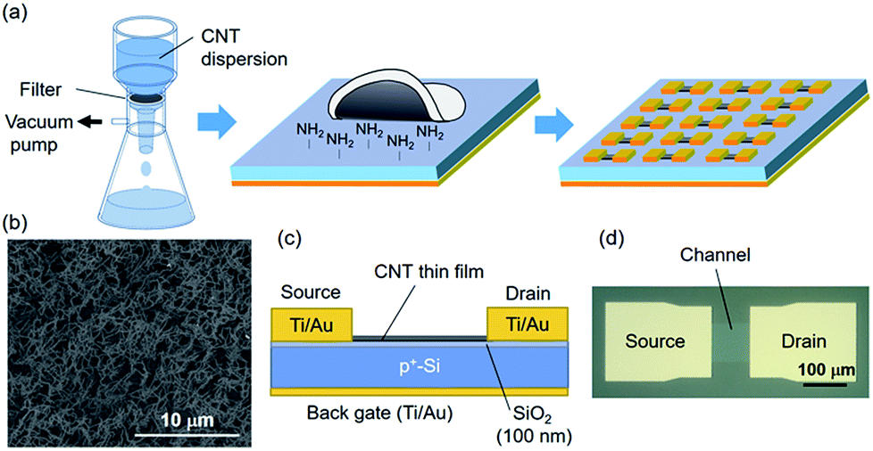 | ||
| Fig. 1 (a) s-CNT TFT fabrication via vacuum suction filtration and transfer. An s-CNTs thin film was formed on a membrane filter by suction filtration and was then transferred onto an APTES-functionalized SiO2/Si substrate. The device fabrication was completed with source/drain formation and CNT patterning. (b) SEM image of CNT film transferred onto the SiO2/Si substrate. (c) and (d) Schematic structure and optical micrograph of a CNT TFT, respectively. | ||
A schematic of the device structure is shown in Fig. 1(c). The source and drain electrodes were formed via photolithography, electron-beam evaporation, and lift-off. Finally, the s-CNTs were patterned by photolithography and oxygen plasma etching. The channel length (L) and width (W) were held constant at 100 μm. To understand the effect of the CNT number density in the channel on the variability of the electrical characteristics, we prepared CNT films with number densities ranging from 51 CNTs per μm2 to 341 CNTs per μm2, which corresponded to 2.5ρth − 16ρth, where ρth is the two-dimensional percolation threshold given by ρth = 4.242/(πLCNT2).30 More than 500 CNT TFTs were produced for each CNT density.
We also investigated the yield and variability of ICs fabricated on a flexible substrate. In this case, bottom-gate CNT TFTs were fabricated on a poly(ethylene naphthalate) (PEN) substrate using the same method as Sun et al.,10 while a s-CNT thin film was employed as the channel.
Results and discussion
Fig. 2(a) shows typical drain current (ID)–drain voltage (VDS) characteristics of a fabricated CNT TFT with a CNT density of 149 CNTs per μm2, exhibiting clear saturation characteristics. Fig. 2(b) depicts the ID–gate voltage (VGS) characteristics of 507 devices measured in the saturation region at VDS = −5 V. All of the devices exhibit normal p-type transfer characteristics, except for several devices that were defective due to failure during the lithography process. The yield was 99.2% (507/511). The average on/off ratio and mobility were ∼105 and 14.1 cm2 V−1 s−1, respectively. The standard deviation of the on-current (ION), which was defined as ID in the saturation region at VDS = −5 V and VGS = −5 V, was fairly small, 21.7%. | ||
| Fig. 2 (a) ID–VDS characteristics of a typical CNT TFT with a CNT density of 149 CNTs per μm2, (b) ID–VGS characteristics of 507 devices at VDS = −5 V. | ||
In general, ION is a function of the threshold voltage (Vth) and transconductance (gm) according to ION = gm(VGS − Vth)/2, where gm = WμC(VGS− Vth)/L and μ and C are the mobility and gate capacitance, respectively. The variation of ION was assessed by evaluating the correlations between ION and Vth and between ION and gm. Fig. 3(a) shows Vth and gm as functions of the square root of ION for the 507 devices shown in Fig. 2(b). Here, Vth was measured by extrapolating a linear fit of the ID1/2–VGS characteristics. The correlation coefficients between ION1/2 and Vth and between ION1/2 and gm are 0.760 and −0.977, respectively, showing that both Vth and gm variations caused ION variations. However, there is a stronger correlation between ION and gm. The plausible cause of the variation of gm is CNT density non-uniformity, i.e. both C and μ are affected by the CNT density.
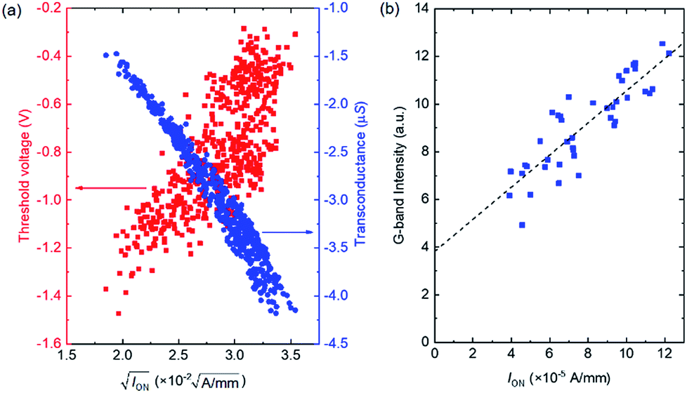 | ||
| Fig. 3 (a) Threshold voltage and transconductance versus ION1/2 for the 507 devices shown in Fig. 2(b). (b) G-band intensity of Raman scattering versus ION of various CNT TFTs. The broken line was obtained via the least squares method. | ||
The correlation between ION and the CNT density was also investigated by performing Raman scattering spectroscopy. In the Raman measurements, the diameter of the excitation laser on the sample was set to 140 μm, and the Raman signal was taken from whole region of the TFT channel, so the Raman intensity was proportional to the amount of CNTs in the channel. Fig. 3(b) shows IONversus the G-band intensity of the Raman scattering for 42 devices. A clear correlation is evident between ION and the G-band intensity with a correlation efficient of 0.87, showing that the ION variation was primarily caused by the variation of the amount of CNTs in the channel.
Fig. 4(a) and (b) present the spatial distribution and histogram of ION, respectively, for 507 devices contained in a quarter of the sample. A macroscopic distribution with dimensions of several millimetres can be seen in the ION map. In the small 5 × 5 mm2 areas labelled area #1 and area #2, which are surrounded by red squares in Fig. 4(a), the standard deviations of the ION distribution were found to be 12.2% (Fig. 4(c)) and 18.9% (Fig. 4(d)), which are less than overall variation mentioned before.
 | ||
| Fig. 4 (a) Spatial distribution of on-current for the 507 devices shown in Fig. 2(b). The average on-current is denoted as μ in the colour scale. VDS = VGS = −5 V. On-current histograms for (b) the whole device and (c) area #1 and (d) area #2 surrounded by red squares in (a). | ||
To determine the potential uniformity without macroscopic variation, we adopted spatial autocorrelation analysis. The spatial autocorrelation (Moran's I), which shows the similarities between distant devices, is given by31
 | (1) |
 | ||
| Fig. 5 Spatial autocorrelation (Moran's I) as a function of distance between CNT TFTs. | ||
The standard deviation of ION, σ(ION), divided by the average ION, μ(ION), is shown as a function of the CNT number density in Fig. 6. The red dots and blue triangles represent the experimentally obtained variations for the overall sample and a 9 mm2 area, respectively. The green squares depict the variations obtained by performing a Monte Carlo simulation. In the simulation, conductive sticks were randomly dispersed in the channel area and ION was calculated by assuming that the contact resistances of the CNT-to-CNT junctions dominated the channel resistance rather than the resistances of the CNTs. We also assumed W = L = 100 μm, LCNT = 0.5 μm, an s-CNT purity of 95%, and a CNT-to-CNT junction resistance of 100 kΩ in the on state. The simulated variations intrinsically originate from the randomness of network-like CNT thin film. This intrinsic variations decrease with increasing CNT density. In the experimental results, however, we obtained two types of variations in addition to the intrinsic variations: the microscopic variations observable in the 9 mm2 area indicated by the blue hatched area in the Fig. 6, which were probably caused by the aggregation of CNTs, as can be seen in the SEM results in Fig. 1(b); and macroscopic variations, as indicated by the red hatched area, which correspond to the ION variations observable in Fig. 4(a).
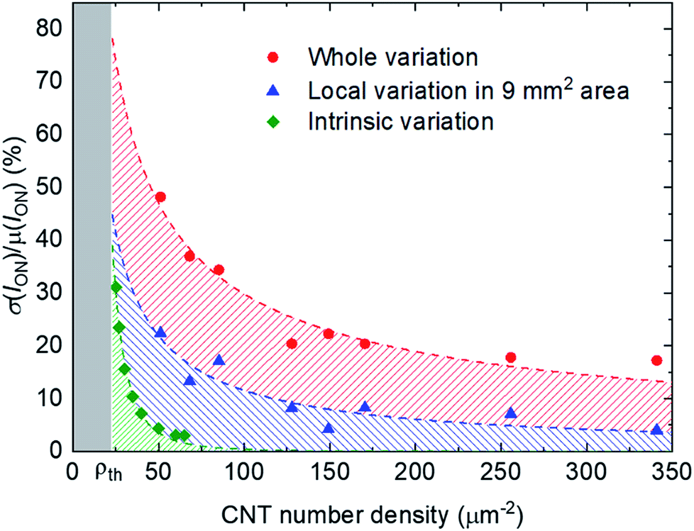 | ||
| Fig. 6 Standard deviation of ION divided by the average ION value as a function of the number density of CNTs in the channel. The red circles and blue triangles are the experimental data obtained for whole devices and devices in a local area of 9 mm2, respectively. The green diamonds represent the data obtained by Monte Carlo simulation. The hatched regions show the macroscopic (red), microscopic (blue), and intrinsic (green) variations. | ||
These additional variations were not reduced by increasing the CNT density. With a CNT density of 149 μm−2, ∼18% (∼6%) of the ION variations were attributed to the macroscopic (microscopic) variations; thus, the macroscopic variations mainly caused the ION variations in this work. The macroscopic variation of ION probably resulted from the film formation via suction filtration, in which the CNT suspension is likely to flow through the membrane filter unevenly due to the surface tension of the droplets on the drain side of the filter. The droplets of filtrated dispersion drop off from some particular sites of the membrane filter, which may cause the biased flow of the dispersion through the membrane filter via the surface tension of the droplets. Controlling the drop-off sites on the membrane filter would be a key to improve the uniformity in the macroscopic scale. In order to reduce the microscopic CNT aggregations, the control of CNT bundling is important. In fact, it was observed from atomic force microscopy that the CNTs were bundled to be 3–4 nm in bundle size. An optimization of CNT dispersion conditions is necessary.
Finally, we investigated the impact of the variability of the TFT characteristics on the yield and variation of logic ICs such as inverters and ring oscillators. Fig. 7(a) and (b) show a photograph and schematic of the device structure of a CNT TFT fabricated on a plastic film. Bottom-gate CNT TFTs were fabricated on a PEN substrate. The gate insulator was 40 nm-thick Al2O3 deposited by atomic layer deposition. W/L was 100/100 μm. Fig. 7(c) shows the transfer characteristics of 825 devices. The TFT yield was found to be 95.0% (825/868), and the ION variation was 27.2%, which is comparable to that on the Si substrate.
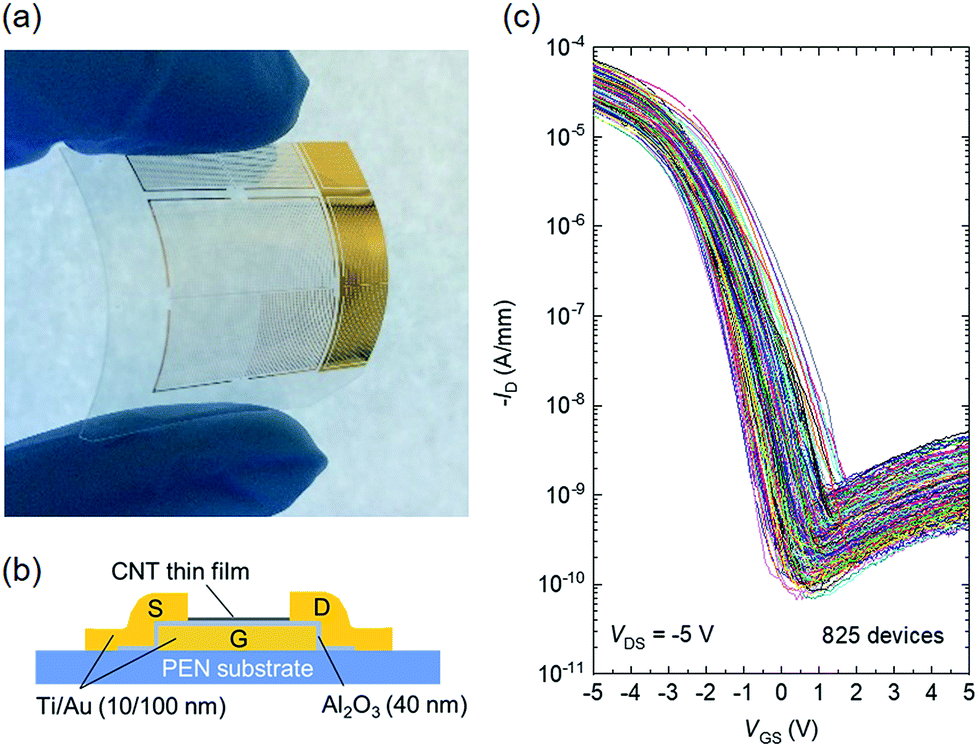 | ||
| Fig. 7 Flexible CNT TFTs. (a) Photograph, (b) schematic device structure, and (c) transfer characteristics of 825 CNT TFTs at VDS = −5 V. | ||
We fabricated inverters with an enhancement/depletion configuration, as shown in the inset of Fig. 8(a). The load TFT was slightly doped with tetrafluoro-tetracyano quinodimethane to shift the threshold voltage into depletion mode. Fig. 8(a) shows the input–output characteristics of an inverter operated at VDD = −5 V. Clear inverter operation was obtained with input–output voltage matching. The threshold voltage is −2.6 V, which is close to the ideal value of VDD/2. The voltage gain is as high as 30.
 | ||
| Fig. 8 Flexible CNT inverters. (a) Transfer characteristics and voltage gain of an inverter. Insets: photograph and circuit diagram. (b) Transfer characteristics and histograms of the (c) voltage gain and (d) threshold voltage of 24 inverters. | ||
Fig. 8(b) shows input–output characteristics of 24 inverters. All of the inverters worked successfully, with an average high voltage gain of 32 and logic threshold voltage of 2.9 V, as shown in the histograms in Fig. 8(c) and (d), respectively. The logic threshold voltage distribution is fairly small compared to those reported recently.32 The logic threshold voltage of an inverter is determined by the difference between the VT values of two transistors in an ideal case; hence, the VT distributions of transistors directly influence the logic threshold voltage variability of inverters. In the present case, however, the logic threshold voltage variability (∼1.5 V difference between the maximum and minimum values) was larger than the distribution of the VT values of the TFTs (∼0.9 V, not shown). In the present case, the gm values of the TFTs were widely distributed due to the non-uniformity of the CNT density, as described before, so the logic threshold voltage was also scattered.
In addition, ring oscillators (with 3, 11, and 21 stages) were fabricated on a PEN substrate, as shown in Fig. 9(a). A photograph and circuit diagram of the 21-stage ring oscillator are provided in Fig. 9(b). The output of the buffer amplifier was measured with an oscilloscope via an instrument amplifier with high input impedance. A typical oscillation waveform is shown in Fig. 9(c). The ring oscillators exhibit oscillations at VDD as low as 2 V due to the local uniformity of the TFT characteristics. The oscillation frequency is 42.5 Hz, corresponding to a switching time of 56 ms for an inverter. The yield of each type of fabricated ring oscillator is shown in Fig. 9(d) as a function of the number of TFTs in the ring oscillator. All of the 3-stage ring oscillators worked; however, the yield decreases as the number of TFTs in the ring oscillator increases, reaching 50% for the 11-stage oscillator (24 TFTs) and 25% for the 21-stage oscillator (44 TFTs). The solid curves in Fig. 9(d) show the calculated IC yields for various TFT yields, y = xN, where x, y, and N represent the TFT yield, IC yield, and number of TFTs in the IC, respectively. The yield curve of the fabricated ring oscillator can be fitted by the calculated yield curve when the TFT yield is 97%. Therefore, the ring-oscillator yield degradation is dominated by the TFT yield rather than by the variability of the TFT characteristics.
 | ||
| Fig. 9 Flexible CNT ring oscillators. (a) Photograph of fabricated ICs. (b) Photograph and circuit diagram of a 21-stage ring oscillator with an output buffer. (c) Output waveform of the 21-stage ring oscillator. (d) Ring oscillator yield as a function of the number of TFTs in the circuit. | ||
The variability of the TFT characteristics, however, directly affected the operation speed of the ring oscillators. The delay time (τ) per stage ranged from 0.81 ms per stage to 2.8 ms per stage, from 0.98 ms per stage to 3.3 ms per stage, and from 0.53 ms per stage to 0.57 ms per stage for the 3-, 11-, and 21-stage oscillators, respectively. The variation of τ decreased as the number of stages in the ring oscillator increased. The standard deviation of τ divided by the average value was 44%, 39%, and 4.3% for the 3-, 11-, and 21-stage oscillators, respectively. The τ value of an inverter is approximately given by τ = WL(CGS + Cp)/gm, where CGS is the channel capacitance and Cp is parasitic capacitance attributed to the overlaps between the gate and source/drain electrodes. Therefore, the gm variation directly affects the τ variation. Note that gm is proportional to CGS and the variations of gm and CGS may cancel one another, causing τ not to be affected; however, this is not the case for the present devices because Cp (∼6 pF) was twice as large than CGS (∼3 pF) in the present device. As the number of stages in a ring oscillator increases, the oscillation frequency variability can decrease because of the averaging effect of a series connection of inverters.
Conclusion
The origins of the variability of the electrical characteristics of CNT TFTs were investigated statistically in this study. The ION distribution exhibited a strong correlation with gm rather than VT, showing that the non-uniformity of the CNT density primarily caused the variability of the TFT characteristics. Spatial autocorrelation analysis revealed that there was millimetre-scale, macroscopic non-uniformity in the CNT density. We also found that even in the local regime where the macroscopic variability was negligible, the variability was larger than that expected from the Monte Carlo simulation. The CNT aggregation caused during CNT film fabrication could be attributed to the microscopic variability. It was expected that by eliminating the macroscopic variations, the ION variations could be reduced to 4.2% within a 9 mm2 area. We also investigated the variability of the properties of ICs such as inverters and ring oscillators fabricated on flexible plastic film. All 24 inverters worked well, and their logic threshold voltage variations were fairly small. As the number of stages in the ring oscillator increased, the ring oscillator yield decreased; however, the oscillation frequency variability was improved due to the averaging effect of the series connection of inverters. Although the carrier mobility of 14.1 cm V−1 s−1 would be satisfactory for some applications such as a backplane of flexible e-papers and low frequency-band radio frequency identification (RFID) tags, an improvement of uniformity of CNT thin films is a key issue to be addressed for the practical applications. Our statistical analysis and results offer an effective way to investigate origins of variability of CNT TFTs and ICs.Conflicts of interest
There are no conflicts to declare.Acknowledgements
The semiconductor SWNTs used in this study were provided by Technology Research Association for Single Wall Carbon Nanotubes. This work was partially supported by the Strategic International Collaborative Research Program (SICORP) of Japan Science and Technology Agency, Japan Society for the Promotion of Science (JSPS) KAKENHI, and JST-CREST.References
- G. H. Gelinck, H. E. A. Huitema, E. van Veenendaal, E. Cantatore, L. Schrijnemakers, J. B. P. H. van der Putten, T. C. T. Geuns, M. Beenhakkers, J. B. Giesbers, B. H. Huisman, E. J. Meijer, E. M. Benito, F. J. Touwslager, A. W. Marsman, B. J. E. van Rens and D. M. de Leeuw, Flexible active-matrix displays and shift registers based on solution-processed organic transistors, Nat. Mater., 2004, 3, 106–110 CrossRef CAS PubMed.
- K. Nomura, H. Ohta, A. Takagi, T. Kamiya, M. Hirano and H. Hosono, Room-temperature fabrication of transparent flexible thin-film transistors using amorphous oxide semiconductors, Nature, 2004, 432, 488–492 CrossRef CAS PubMed.
- D. H. Kim, J. Viventi, J. J. Amsden, J. Xiao, L. Vigeland, Y. S. Kim, J. A. Blanco, B. Panilaitis, E. S. Frechette, D. Contreras, D. L. Kaplan, F. G. Omenetto, Y. Huang, K. C. Hwang, M. R. Zakin, B. Litt and J. A. Rogers, Dissolvable films of silk fibroin for ultrathin conformal bio-integrated electronics, Nat. Mater., 2010, 9, 511–517 CrossRef CAS PubMed.
- A. Javey, J. Guo, Q. Wang, M. Lundstrom and H. J. Dai, Ballistic carbon nanotube field-effect transistors, Nature, 2003, 424, 654–657 CrossRef CAS PubMed.
- M. M. J. Treacy, T. W. Ebbesen and J. M. Gibson, Exceptionally high Young's modulus observed for individual carbon nanotubes, Nature, 1996, 381, 678–680 CrossRef CAS.
- E. S. Snow, P. M. Campbell, M. G. Ancona and J. P. Novak, High-mobility carbon-nanotube thin-film transistors on a polymeric substrate, Appl. Phys. Lett., 2005, 86, 033105 CrossRef.
- C. Wang, J. Zhang, K. Ryu, A. Badmaev, L. Gomez de Arco and C. Zhou, Wafer-scale fabrication of separated carbon nanotube thin-film transistors for display applications, Nano Lett., 2009, 9, 4285–4291 CrossRef CAS PubMed.
- B. Tian, X. Liang, Q. Yan, H. Zhang, J. Xia, G. Dong, L. Peng and S. Xie, Wafer scale fabrication of carbon nanotube thin film transistors with high yield, J. Appl. Phys., 2016, 120, 034501 CrossRef.
- S. G. Bucella, J. M. Salazar-Rios, V. Derenskyi, M. Fritsch, U. Scherf, M. A. Loi and M. Caironi, Inkjet printed single-walled carbon nanotube based ambipolar and unipolar transistors for high-performance complementary logic circuits, Adv. Electron. Mater., 2016, 2, 1600094 CrossRef.
- D. M. Sun, M. Y. Timmermans, Y. Tian, A. G. Nasibulin, E. I. Kauppinen, S. Kishimoto, T. Mizutani and Y. Ohno, Flexible high-performance carbon nanotube integrated circuits, Nat. Nanotechnol., 2011, 6, 156–161 CrossRef CAS PubMed.
- D. M. Sun, M. Y. Timmermans, A. Kaskela, A. G. Nasibulin, S. Kishimoto, T. Mizutani, E. I. Pauppinen and Y. Ohno, Mouldable all-carbon integrated circuits, Nat. Commun., 2013, 4, 2302 CrossRef PubMed.
- Q. Cao, H. Kim, N. Pimparkar, J. P. Kulkarni, C. Wang, M. Shim, K. Roy, M. A. Alam and J. A. Rogers, Medium-scale carbon nanotube thin-film integrated circuits on flexible plastic substrates, Nature, 2008, 454, 495–500 CrossRef CAS PubMed.
- M. L. Geier, J. J. McMorrow, W. Xu, J. Zhu, C. H. Kim, T. J. Marks and M. C. Hersam, Solution-processed carbon nanotube thin-film complementary static random access memory, Nat. Nanotechnol., 2015, 10, 944–948 CrossRef CAS PubMed.
- H. Chen, Y. Cao, J. Zhang and C. Zhou, Large-scale complementary macroelectronics using hybrid integration of carbon nanotubes and IGZO thin-film transistors, Nat. Commun., 2014, 5, 4097 CrossRef CAS PubMed.
- M. Ishida and F. Nihey, Estimating the yield and characteristics of random network carbon nanotube transistors, Appl. Phys. Lett., 2008, 92, 163507 CrossRef.
- A. Kaskela, K. Mustonen, P. Laiho, Y. Ohno and E. I. Kauppinen, Toward the limits of uniformity of mixed metallicity SWCNT TFT arrays with spark-synthesized and surface-density-controlled nanotube networks, ACS Appl. Mater. Interfaces, 2015, 7, 28134–28141 CrossRef CAS PubMed.
- T. Tanaka, H. Jin, Y. Miyata and H. Kataura, High-yield separation of metallic and semiconducting single-wall carbon nanotubes by agarose gel electrophoresis, Appl. Phys. Express, 2008, 1, 114001 CrossRef.
- M. S. Arnold, A. A. Green, J. F. Hulvat, S. I. Stupp and M. C. Hersam, Sorting carbon nanotubes by electronic structure using density differentiation, Nat. Nanotechnol., 2006, 1, 60–65 CrossRef CAS PubMed.
- M. Zheng, A. Jagota, M. S. Strano, A. P. Santos, P. Barone, S. G. Chou, B. A. Diner, M. S. Dresselhaus, R. S. Mclean, G. B. Onoa, G. G. Samsonidze, E. D. Semke, M. Usrey and D. J. Walls, Structure-based carbon nanotube sorting by sequence-dependent DNA assembly, Science, 2003, 302, 1545–1548 CrossRef CAS PubMed.
- C. Y. Khripin, J. A. Fagan and M. Zheng, Spontaneous partition of carbon nanotubes in polymer-modified aqueous phases, J. Am. Chem. Soc., 2013, 135, 6822–6825 CrossRef CAS PubMed.
- M. D. Lay, J. P. Novak and E. S. Snow, Simple route to large-scale ordered arrays of liquid-deposited carbon nanotubes, Nano Lett., 2004, 4, 603–606 CrossRef CAS.
- N. Saran, K. Parikh, D. S. Suh, E. Munoz, H. Kolla and S. K. Manohar, Fabrication and characterization of thin films of single-walled carbon nanotube bundles on flexible plastic substrates, J. Am. Chem. Soc., 2004, 126, 4462–4463 CrossRef CAS PubMed.
- C. M. Trottier, P. Glatkowski, P. Wallis and J. Luo, Properties and characterization of carbon-nanotube-based transparent conductive coating, J. Soc. Inf. Disp., 2005, 13, 759–763 CrossRef CAS.
- M. Shimizu, S. Fujii, S. Asano, T. Tanaka and H. Kataura, Fabrication of homogeneous thin films of semiconductor-enriched single-wall carbon nanotubes for uniform-quality transistors by using immersion coating, Appl. Phys. Express, 2013, 6, 105103 CrossRef.
- S. Ohmori, K. Ihara, F. Nihey, Y. Kuwahara and T. Saito, Low variability with high performance in thin-film transistors of semiconducting carbon nanotubes achieved by shortening tube lengths, RSC Adv., 2012, 2, 12408 RSC.
- T. Tanaka, H. Jin, Y. Miyata, S. Fujii, H. Suga, Y. Naitoh, T. Minari, T. Miyadera, K. Tsukagoshi and H. Kataura, Simple and scalable gel-based separation of metallic and semiconducting carbon nanotubes, Nano Lett., 2009, 9, 1497–1500 CrossRef CAS PubMed.
- Y. Miyata, K. Yanagi, Y. Maniwa and H. Kataura, Optical evaluation of the metal-to-semiconductor ratio of single-wall carbon nanotubes, J. Phys. Chem. C, 2008, 112, 13187–13191 CrossRef CAS.
- R. B. Weisman and S. M. Bachilo, Dependence of optical transition energies on structure for single-walled carbon nanotubes in aqueous suspension: An empirical Kataura plot, Nano Lett., 2003, 3, 1235–1238 CrossRef CAS.
- M. C. LeMieux, M. Roberts, S. Barman, Y. W. JIn, J. M. Kim and Z. Bao, Self-sorted, aligned nanotube networks for thin-film transistors, Science, 2008, 321, 101–104 CrossRef CAS PubMed.
- C. Kocabas, N. Pimparkar, O. Yesilyurt, S. J. Kang, M. A. Alam and J. A. Rogers, Experimental and theoretical studies of transport through large scale, partially aligned arrays of single-walled carbon nanotubes in thin film type transistors, Nano Lett., 2007, 7, 1195–1202 CrossRef CAS PubMed.
- P. A. P. Moran, Notes on continuous stochastic phenomena, Biometrika, 1950, 37, 17–23 CrossRef CAS PubMed.
- B. Y. Chen, P. Zhang, L. Ding, J. Han, S. Qiu, Q. Li, Z. Zhang and L. M. Peng, Highly uniform carbon nanotube field-effect transistors and medium scale integrated circuits, Nano Lett., 2016, 16, 5120–5128 CrossRef CAS PubMed.
| This journal is © The Royal Society of Chemistry 2019 |