
 Open Access Article
 This Open Access Article is licensed under a Creative Commons Attribution-Non Commercial 3.0 Unported Licence
Pulsed laser deposition of single-layer MoS2 on Au(111): from nanosized crystals to large-area films†
Francesco
Tumino
 *,
Carlo S.
Casari
,
Matteo
Passoni
,
Valeria
Russo
and
Andrea
Li Bassi
*,
Carlo S.
Casari
,
Matteo
Passoni
,
Valeria
Russo
and
Andrea
Li Bassi
Department of Energy, Politecnico di Milano, Piazza Leonardo da Vinci 32, 20133 Milano, Italy. E-mail: francesco.tumino@polimi.it
First published on 25th October 2018
Abstract
Molybdenum disulphide (MoS2) is a promising material for heterogeneous catalysis and novel two-dimensional (2D) optoelectronic devices. In this work, we synthesized single-layer (SL) MoS2 structures on Au(111) by pulsed laser deposition (PLD) under ultra-high vacuum (UHV) conditions. By controlling the PLD process, we were able to tune the sample morphology from low-coverage SL nanocrystals to large-area SL films uniformly wetting the whole substrate surface. We investigated the obtained MoS2 structures at the nanometer and atomic scales by means of in situ scanning tunneling microscopy/spectroscopy (STM/STS) measurements, to study the interaction between SL MoS2 and Au(111)—which for example influences MoS2 lattice orientation—the structure of point defects and the formation of in-plane MoS2/Au heterojunctions. Raman spectroscopy, performed ex situ on large-area SL MoS2, revealed significant modifications of the in-plane E12g and out-of-plane A1g vibrational modes, possibly related to strain and doping effects. Charge transfer between SL MoS2 and Au is also likely responsible for the total suppression of excitonic emission, observed by photoluminescence (PL) spectroscopy.
1 Introduction
Transition metal dichalcogenides (TMDs) are solid materials composed of weakly interacting layers which can be isolated from the bulk. Single layers of TMDs represent an important class of two-dimensional (2D) crystals, normally composed of one atomic plane of transition metal atoms, sandwiched by two hexagonal planes of chalcogen atoms.1 Single-layer molybdenum disulphide (SL MoS2) is a prominent member of this family, showing intriguing electronic and optical properties, such as a direct band gap in the visible range (1.9 eV),2 strong photoluminescence3 and high carrier mobility,4 which are extremely promising for future low-dimensional optoelectronic devices. Moreover, the catalytic properties of MoS2 have been intensively studied for applications in hydrodesulfurization processes and the hydrogen evolution reaction.5,6 The study of low-dimensional MoS2 structures has greatly benefited from surface science investigations of model nanoscale MoS2 systems fabricated by Molecular Beam Epitaxy (MBE) on suitable substrates, such as Au(111).7–12 This experimental approach enables the application of high spatial resolution techniques, such as scanning tunneling microscopy (STM) and spectroscopy (STS), to characterize in situ the fundamental structural and electronic properties of SL MoS2 under controlled ultra-high vacuum (UHV) conditions. Metal-supported MoS2 nanostructures also allow the study of the nanoscale properties of MoS2/metal heterostructures, which are of great interest for future MoS2-based electronic devices. The effects induced by metal interaction on the MoS2 properties have been addressed by recent studies,13–16 showing a significant influence of metal–MoS2 contact on the interface electronic structure. However, the possible influence on morphological and structural properties has not been extensively investigated, e.g. regarding MoS2 lattice orientation, moiré superstructures and lattice defects. The metallic substrate may also induce strain in supported MoS2, affecting its vibrational and optoelectronic properties. In this regard, Raman and photoluminescence (PL) spectroscopy, although not usually applied in combination with in situ surface characterization techniques, may provide valuable experimental information, having been found to show high sensitivity to thickness,2,17 strain18,19 and doping20,21 in SL and few-layer MoS2 flakes.Although model systems of metal-supported MoS2 nanocrystals offer access to the study of nano- and atomic-scale MoS2 properties, the application of 2D MoS2 in real devices requires the synthesis and characterization of large-area films on the centimeter scale. Therefore, studying in situ the growth of SL MoS2 nanocrystals into large-area structures would provide a more complete understanding of SL MoS2 properties, allowing bridging of the gap between model nanoscale systems and more realistic ones. To this purpose, we need to develop synthesis methods allowing tuning of the growth of MoS2 structures in the monolayer (ML) range, while meeting the high standards of sample purity and surface quality required by in situ surface science investigations. The synthesis of large-area MoS2 films has been a major research task over the last few years, having as its main objective the development of effective and scalable bottom-up approaches able to overcome the intrinsic limitations of top-down exfoliation methods, such as the relatively small size of produced crystals and the poor control of their morphological and structural properties. Recently, the pulsed laser deposition (PLD) technique has shown great potential for the growth of 2D MoS2 (ref. 22–25) and other multi-elemental 2D materials (e.g. WS2,26 MoSe2,27 GaSe,28 and ZnO29), providing the capability of high-throughput and centimeter-scale growth with precise control of the thickness and morphology. The PLD working principle is conceptually simple: the ablation of a solid target by high energy laser pulses produces a plasma plume of ejected species which condenses on the substrate, placed a few centimeters in front of the target. PLD offers several advantages in comparison to more conventional chemical vapor deposition (CVD) or molecular beam epitaxy (MBE) techniques. For instance, under suitable conditions, stoichiometric transfer of ablated species from the target to the substrate can be achieved, a key property which makes PLD suitable for the stoichiometric growth of multi-element materials, avoiding use of expensive and potentially dangerous precursors (e.g. H2S) on which other synthesis methods rely.10,12,30 Moreover, PLD depends on several process parameters (e.g. laser energy, total number of ablating laser pulses, pulse repetition rate, and background gas pressure) which can be properly tuned to control the morphology and structure of deposited materials. Despite its versatility, PLD is not traditionally used in the framework of experimental surface science, where more conventional deposition techniques (e.g. molecular beam epitaxy) are employed. However, the combination of PLD with in situ surface science techniques is highly desirable because it merges together the possibility of conducting detailed nanoscale investigations with high flexibility in tuning the surface morphology and characteristic dimensions of the investigated structures.
In this work, we combine different characterization techniques, i.e. in situ STM/STS, Raman and PL spectroscopy, to study SL MoS2 structures synthesized by PLD on the Au(111) surface under UHV conditions. Au(111) is a well-known surface,31,32 suitable to serve as a model template for STM of supported nanomaterials,33 as well as a platform for investigating the properties of MoS2/metal heterostructures. We developed a PLD-based procedure resulting in the synthesis of SL MoS2 nanocrystals, which we investigated by STM at the nanometer and atomic scales. Our observations allowed us to study interesting properties, such as the relation between the substrate and MoS2 lattice orientation, point defects on the MoS2 surface, and in-plane MoS2/Au heterojunctions originating from partial embedding of MoS2 nanocrystals in the Au topmost layer. Moreover, we explored different PLD-based procedures, being able to finely increase the MoS2 coverage to get a homogeneous SL film over the whole substrate area (about 1 cm2). In addition to STM/STS measurements, Raman and PL spectroscopy provided useful information on the vibrational and optoelectronic properties of the PLD-grown SL MoS2 film on Au(111), revealing possible strain- and doping-induced effects.
2 Experimental
An UHV system (base pressure 2 × 10⁻¹¹ mbar) composed of three interconnected chambers was used for substrate cleaning, PLD, post-deposition annealing and STM/STS characterization.All experiments were performed using Au(111) on mica (Phàsis) as a substrate for MoS2 growth. The substrate was cleaned by cycles of Ar+ sputtering (1 keV) and annealing at 700 K, yielding a pristine Au(111) surface, characterized by the well-known herringbone reconstruction, as verified by STM observations. The Au(111) reconstruction originates from anisotropic compression along 〈1![[1 with combining macron]](https://www.rsc.org/images/entities/char_0031_0304.gif) 0〉 directions that allows accommodation of 23 atoms per cell in 22 bulk lattice sites. At the same time some atoms are pushed aside in the 〈11
0〉 directions that allows accommodation of 23 atoms per cell in 22 bulk lattice sites. At the same time some atoms are pushed aside in the 〈11![[2 with combining macron]](https://www.rsc.org/images/entities/char_0032_0304.gif) 〉 direction in hcp sites instead of the usual fcc ones. This arrangement results in a
〉 direction in hcp sites instead of the usual fcc ones. This arrangement results in a  reconstruction. The atoms in between the two different stacking positions are forced to occupy bridge sites and lift up with respect to the surface plane, forming a couple of ridges (discommensuration lines) which separates hcp regions from fcc ones. As a consequence of surface stress relaxation, the ridges form the typical zig-zag pattern of the herringbone reconstruction.31–33
MoS2 depositions were performed in vacuum in a dedicated PLD chamber (base pressure 5 × 10⁻⁹ mbar), by ablating a rotating MoS2 target (Testbourne) with a KrF laser emitting 20 ns pulses (248 nm wavelength) at a repetition rate of 1 pulse per second. The target was ablated for ∼5 minutes in order to clean its surface before every deposition. Target ablation was achieved with a pulse energy of 100 mJ and a laser fluence in the range 0.5–1.5 J cm−2. During deposition, the substrate was kept at room temperature and placed 5 cm from the target.
After PLD, the sample was internally transferred to a preparation chamber (base pressure 2 × 10⁻¹¹ mbar) where thermal treatments were performed under UHV conditions using an e-beam heater. Annealing temperatures in the range 560–810 K were kept constant for about 30 minutes and measured with a thermocouple close to the sample plate and an external optical pyrometer focused on the sample surface.
Room-temperature STM/STS measurements were performed with an Omicron VT-SPM in a dedicated analysis chamber (base pressure 2 × 10⁻¹¹ mbar), using homemade electrochemically etched W tips. STM images were acquired in constant-current mode and analyzed using software for SPM data analysis (Gwyddion34). The bias voltage (referring to the sample voltage) and current set-point are reported in the figure captions. The differential conductivity (dI/dV) was measured using a lock-in amplifier applying a modulation voltage of 28 mVrms at 4 kHz. I(V) and dI/dV(V) curves were acquired simultaneously under open feedback-loop conditions, using 2 V and 0.4 nA as set-point parameters.
The surface coverage of MoS2 structures, expressed in equivalent Mono-Layers (ML), was estimated from large-scale STM images, by measuring the fraction of the substrate area covered by single-layer MoS2.
A Renishaw InVia spectrometer, coupled with an Ar laser, was used for Raman and PL measurements, which were performed ex situ with a 1 mW excitation at 457 nm and 514.5 nm wavelengths, respectively, through a 50× objective. The spot diameter of the laser on the sample is about 1–2 μm. Ten accumulations of 10 seconds are sufficient to obtain a good signal-to-noise ratio and all the presented results were obtained with that measurement time. Raman measurements were also performed on a natural bulk MoS2 crystal (SPI Supplies) for comparison purposes.
3 Results and discussion
This section is divided into three subsections: in Section 3.1, we discuss the growth of SL MoS2 nanostructures on Au(111), obtained by means of PLD and different post-deposition annealing treatments. In Section 3.2, we focus on the morphological and structural properties of SL MoS2 nanocrystals with the analysis of high resolution STM measurements. In Section 3.3, we elucidate possible routes for the PLD synthesis of large-area SL MoS2 films on Au(111) and we discuss the basic properties revealed by STM, STS, Raman and PL spectroscopy.3.1 Growth of single-layer MoS2 on Au(111)
To investigate the PLD growth of MoS2 on Au(111), we deposited MoS2 on the substrate at room temperature and then performed post-annealing treatments at different temperatures. Preliminary experiments allowed us to optimize the preparation procedure, finding suitable values for process parameters, such as laser pulse energy, number of laser pulses and post-annealing duration. Each deposition was carried out on a freshly cleaned Au(111) surface with 20 laser pulses on the MoS2 target, in order to deposit approximately the same amount of material per deposition. The as-deposited samples were then annealed in UHV for 30 minutes at different temperatures in the range 560–810 K. The obtained results are reported in Fig. 1. | ||
Fig. 1 (a) STM image of the Au(111) surface, showing the typical herringbone reconstruction. Bias voltage and current set-point: V = 0.6 V, I = 1 nA. Inset: atomic resolution STM image highlighting the two different stacking regions, i.e. fcc and hcp, induced by the  reconstruction. (b)–(e) 100 × 100 nm2 size STM images of different MoS2/Au(111) samples obtained after (b) PLD at room temperature (V = 1.93 V, I = 0.5 nA), followed by post-annealing at (c) 560 K (V = −1 V, I = 0.4 nA), (d) 640 K (V = 0.5 V, I = 0.4 nA), (e) 720 K (V = 1 V, I = 0.4 nA) and (f) 810 K (V = 1.2 V, I = 0.3 nA). In (e): blue arrows indicate seemingly thicker nanocrystals composed of SL MoS2 growing on top of one-atom-thick Au islands of the same shape; the green arrow indicates a relatively large nanocrystal attached to the Au step edge; inset: apparent height of MoS2 nanocrystals measured for different bias voltages. In (f): the green arrow indicates a partial embedded SL MoS2 nanocrystal; inset: topographic profile along the white dashed line. reconstruction. (b)–(e) 100 × 100 nm2 size STM images of different MoS2/Au(111) samples obtained after (b) PLD at room temperature (V = 1.93 V, I = 0.5 nA), followed by post-annealing at (c) 560 K (V = −1 V, I = 0.4 nA), (d) 640 K (V = 0.5 V, I = 0.4 nA), (e) 720 K (V = 1 V, I = 0.4 nA) and (f) 810 K (V = 1.2 V, I = 0.3 nA). In (e): blue arrows indicate seemingly thicker nanocrystals composed of SL MoS2 growing on top of one-atom-thick Au islands of the same shape; the green arrow indicates a relatively large nanocrystal attached to the Au step edge; inset: apparent height of MoS2 nanocrystals measured for different bias voltages. In (f): the green arrow indicates a partial embedded SL MoS2 nanocrystal; inset: topographic profile along the white dashed line. | ||
Fig. 1(a) shows an STM image of the Au(111) surface with the characteristic pattern of the herringbone ridges, separating fcc from hcp regions (inset). Immediately after MoS2 deposition (Fig. 1(b)), the substrate is completely covered by a nanostructured film having disordered surface morphology. The deposited structures assume a more regular aspect after annealing: in the range 560–640 K (Fig. 1(c) and (d)), we observe the gradual formation of triangular islands with ∼3 nm sides on average.
For temperatures of around 700 K (Fig. 1(e)) we observe isolated MoS2 nanocrystals with a well-defined geometrical shape and surface morphology. Relatively large nanocrystals (of about 30 nm in linear size) grow attached to Au step edges and clearly show a surface hexagonal moiré pattern (see for example the nanocrystal indicated by the green arrow in Fig. 1(e)). STM allowed us to measure the height of MoS2 islands with respect to the substrate. In this regard, it is important to remark that STM topography is also affected by the local surface electronic properties; therefore, height measurements in general depend on the applied tip–sample voltage. Indeed, we observed that the average apparent height of MoS2 islands varies slightly with bias voltage: the inset plot in Fig. 1(e) shows a variation from a maximum of 2.5 Å to a minimum of 1.6 Å as bias voltage is decreased from 1 V toward the Fermi level (0 V). This variation may be related to the expected semiconducting behavior of MoS2, which causes a low density of states (hence low tunneling current) around the Fermi level. Our measurements are in agreement with previously reported STM data,7,9,30 in which similar MoS2 nanocrystals on Au(111) were attributed to a single S–Mo–S layer. Interestingly, the measured MoS2 thickness is significantly low compared with the known interlayer distance in bulk MoS2 (6.15 Å (ref. 35 and 36)) and with available STM measurements of SL MoS2 on other substrates, e.g. 5–9 Å (depending on bias voltage) on bilayer graphene37 and 6.7 Å on graphite.38 The lower apparent height of SL MoS2 on Au may be due to stronger interaction with the substrate or an interface tunnel barrier13,14 which reduces the tip–sample tunneling conductivity.
From Fig. 1(e) we also notice that some nanocrystals seem to be thicker (e.g. those indicated by blue arrows), showing brighter contrast in STM images. The measured height difference with respect to the other SL islands is ∼2.5 Å, independent of bias voltage and current set-point. This height value agrees well with the monoatomic step height of Au(111), suggesting that brighter islands are composed of SL MoS2 growing on top of small one-atom-thick Au terraces, having exactly the same shape as that of the overlying nanocrystal. This growth mechanism could be induced by stress release effects in the Au surface, triggered by MoS2 nucleation and growth.30 To support this interpretation, we note that MoS2 perturbs the regular arrangement of the herringbone reconstruction, growing on either fcc or hcp Au regions (Fig. 1(e) and (f)). In addition, we rule out the hypothesis that brighter islands in Fig. 1(e) may be associated with bi-layer MoS2 structures: as we will show in the following, 2nd layer growth was observed at higher MoS2 coverages and the STM-measured distance between the 2nd and 1st layers is above 6 Å, in agreement with the 6.15 Å bulk interlayer distance.
By comparing Fig. 1(d)–(f), we observe that the increase of annealing temperature causes noticeable reduction of MoS2 surface coverage, probably due to re-evaporation. Expressing MoS2 coverage in fractions of equivalent mono-layers (ML)—with 1 ML corresponding to SL MoS2 completely covering the Au surface—from large-scale STM images we can estimate a reduction from 0.33 ML to 0.1 ML as the temperature increases from 640 K to 810 K.
As far as morphological properties are concerned, higher annealing temperatures favor the formation of SL MoS2 nanocrystals partially embedded in the Au topmost layer, as indicated by the green arrow in Fig. 1(f). By “partially embedded”, we mean that such islands lie on top of a one-step lower Au patch, with respect to the surrounding Au terrace. Indeed, the line profile inset in Fig. 1(f) shows that the MoS2 surface, corrugated by the moiré pattern, is approximately at the same level as that of the surrounding Au terrace. The growth of partially embedded SL MoS2 islands causes the formation of in-plane Au/MoS2 interfaces of peculiar morphology, which will be further discussed in the following.
3.2 Atomic-scale properties of MoS2 nanocrystals
Higher resolution STM images allowed us to study in more detail the morphological and structural properties of the observed nanocrystals. On the basis of the STM observations previously discussed, we focused our study on samples annealed at temperatures above 700 K. As shown by the STM image in Fig. 2(a), the majority of observed SL nanocrystals are triangularly shaped, although they usually show slightly truncated corners. Following the path of Au herringbone ridges, we can see that MoS2 islands grow on either fcc or hcp domains, thus distorting the otherwise regular herringbone pattern. | ||
| Fig. 2 (a) STM image of SL MoS2 nanocrystals on Au(111) (V = 1 V, I = 0.3 nA). (b) Atomic resolution STM image of a triangular nanocrystal, showing the surface hexagonal atomic lattice (V = 0.3 V, I = 1 nA). Inset: details of the MoS2 lattice where both S atoms (yellow dots) and Mo atoms (blue dots) are visible. (c) STM image of two differently oriented triangular nanocrystals: the one on the left grows on the hcp region, while the other on the fcc one (V = 0.6 V, I = 1 nA). (d) STM image showing triangular nanocrystals, differently oriented, which merge together forming 60° domain boundaries (indicated by black arrows) (V = 1 V, I = 0.3 nA). (e) and (f) Atomistic models of the MoS2 lattice on fcc and hcp Au substrates, respectively. Color code: S = yellow, Mo = blue, 1st layer Au = red, 2nd layer Au = grey, 3rd layer Au = green. The white dashed triangles indicate the orientation of the MoS2 unit cell. | ||
Atomic resolution STM images (Fig. 2(b)) allowed us to measure a lattice parameter of 3.18 ± 0.05 Å. Within measurement uncertainty, this value agrees with the in-plane lattice constant of unstrained 2H–MoS2(0001).35,36 The MoS2 atomic corrugation observed with STM is mostly due to surface S atoms,39,40 which are imaged as the brightest spots in atomic resolution images (yellow dots in the inset of Fig. 2(b)). We can also observe less bright spots in trigonal configuration with three nearest neighbor S atoms, which are ascribable to Mo atoms41,42 (blue dots in the inset of Fig. 2(b)). The bright brim observed at the island borders can be attributed to one-dimensional metallic edge states.43,44
Our STM images reveal that triangular islands lying in different stacking regions are oppositely oriented, as highlighted in Fig. 2(b). In some cases, differently oriented islands are observed to merge together, forming 60° domain boundaries, as shown for instance in Fig. 2(c). These observations suggest a correlation between the MoS2 lattice orientation and the Au stacking configuration. We can qualitatively interpret this effect by considering the occupation sites of S and Mo atoms on fcc and hcp Au domains. Because on-top atomic sites have been predicted to be the most stable for S atoms in contact with Au,16 we can reasonably assume that, in the first stages of island nucleation and growth, S atoms preferentially occupy on-top (or quasi-on-top) positions. The situation is pictured in Fig. 2(d) and (e) for fcc and hcp domains, respectively. In this representation we assumed, without lack of generality, that Mo atoms (blue dots) lie on the vertical of 2nd layer Au atoms (grey dots). Under the hypothesis that this arrangement of Mo atoms corresponds to the most stable configuration, we clearly see that the MoS2 lattice undergoes a 60° rotation as Au stacking changes from fcc to hcp. Our interpretation implies that Mo atoms in MoS2 strongly interact with Au atoms, and this interaction significantly affects the epitaxial relation between Au(111) and MoS2.
The lattice mismatch between MoS2 and Au(111) generates a hexagonal moiré superlattice. The characteristic pattern of moiré spots is clearly observed on the surface of larger SL MoS2 nanocrystals, growing mostly at Au step edges (Fig. 3(a)) or partially embedded in the Au surface (Fig. 3(e)). The analysis of atomic resolution images and their Fourier transforms allows us to study the geometrical interplay between the substrate and the overlayer lattices, giving rise to the observed moiré pattern. For instance, Fig. 3(b) shows an atomic resolution image of the nanocrystal in Fig. 3(a). Details of its 2D Fast Fourier Transform (FFT) are reported in Fig. 3(c), showing the reciprocal lattice spots ascribable to MoS2 and moiré. According to the schematic picture in Fig. 3(d) (not to scale), we can measure the lengths and relative orientation of MoS2 and moiré lattice vectors. Usually, we obtain 3.18 ± 0.05 Å for MoS2, 33 ± 1 Å for the moiré, and a small angle of 2° ± 1° between the two.
 | ||
| Fig. 3 (a) STM image of a SL MoS2 nanocrystal showing the characteristic moiré pattern (V = 0.5 V, I = 0.5 nA). (b) Atomic resolution STM image of the nanocrystal shown in (a) (V = 0.1 V, I = 1 nA). (c) Details of the 2D Fast Fourier Transform (FFT) of the STM image in (b), showing two opposite spots of the MoS2 hexagon, surrounded by the moiré lattice spots. The red arrow denotes the MoS2 reciprocal lattice vector. (d) Schematic representation of the spot arrangement (not to scale): GMoS2 and Gmoiré are the reciprocal vectors of MoS2 and moiré lattices, respectively. (e) Partially embedded SL MoS2 nanocrystal growing over a Au(111) grain boundary (V = 1 V, I = 0.3 nA). Labels α and β denote two different moiré patterns. The white arrow indicates a screw dislocation of the substrate. (f) Atomic resolution STM image of the white frame in (e) (V = 0.5 V, I = 0.5 nA). Inset: 2D FFT of the STM image showing the hexagon of sharp spots associated with the MoS2 lattice. (g) Details of the 2D FFT of the α and β patterns. Scale bars of FFTs: 1 nm−1. | ||
Occasionally, different moiré patterns can be observed on nanocrystals growing over Au grain boundaries. One example is shown in Fig. 3(e), where a partially embedded nanocrystal lies over the boundary between differently oriented Au(111) domains (a screw dislocation can also be seen in the lower right part of the image, indicated by a white arrow). The moiré pattern clearly changes in both periodicity and orientation from the α region to the β one (see labels in Fig. 3(e)). Interestingly, atomic resolution images taken across the interface between the two regions (Fig. 3(f)) do not show any discontinuity or orientation change of the MoS2 surface lattice. This is also confirmed by the 2D FFT inset in Fig. 3(f) where a single hexagon of sharp spots is revealed, yielding the usual ∼3.18 Å parameter. We performed a local Fourier analysis to study the moiré geometry in α and β (Fig. 3(g)). The moiré periodicity is 31.5 ± 0.5 Å in α and 19.5 ± 2 Å in β, while the angle formed with the MoS2 lattice vector is 15° ± 1° in α and 54° ± 1.5° in β. These measurements suggest that the substrate grain boundary does not induce any perturbation in the MoS2 lattice but a rigid in-plane rotation in order to accommodate the substrate orientation change. As a consequence, the rotation angle between MoS2 and Au(111) must be different in the three cases, i.e. the usual structure (Fig. 3(b)) and the α and β structures (Fig. 3(f)). This angle can be derived using a theoretical description of the superlattice based on the geometric characteristics of the substrate and overlayer.45 We obtained a very small angle of 0.2° ± 0.1° between MoS2 and Au(111) in the case of the usual moiré pattern, and, as expected, larger values for α and β patterns: 1.4° ± 0.1° and 7° ± 1°, respectively. Fig. 4 shows an atomistic representation of the three different structures, obtained by rotating the MoS2 lattice (lattice constant: 3.18 Å) with respect to the Au surface (lattice constant: 2.89 Å) by the previously reported rotation angles. Black arrows represent the moiré lattice vectors calculated starting from the relation Gmoiré = GAu − GMoS2 between the reciprocal lattice vectors.45 The observed behavior of MoS2 nanocrystals over a substrate grain boundary is likely the result of an energetic balance among strong intralayer covalent interactions and the interaction with the substrate. The former are likely responsible for the preservation of the MoS2 crystal structure over the substrate boundary, while the latter induces a change in the MoS2 lattice orientation.
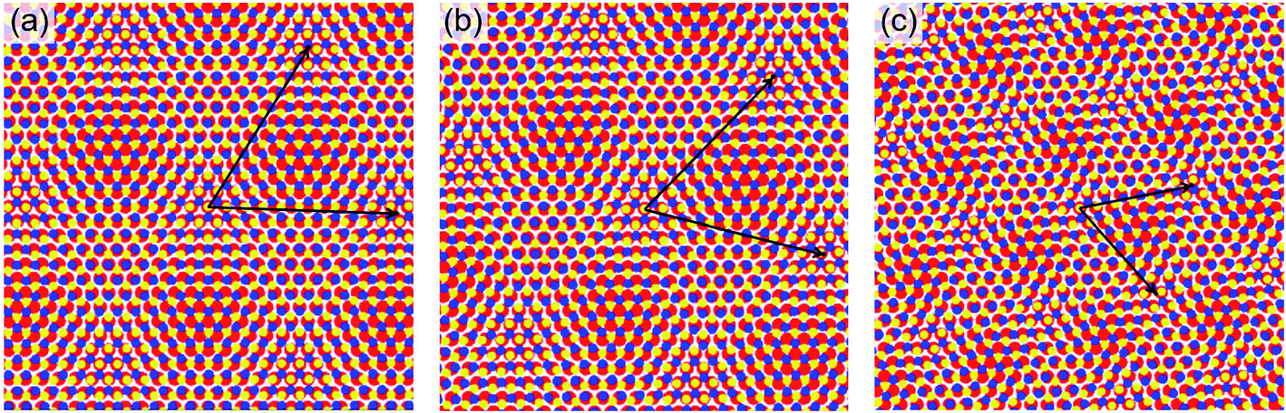 | ||
| Fig. 4 Atomistic models of (a) the usually observed moiré pattern, and (b) the α and (c) β patterns shown in Fig. 3(e) and (f). Black arrows represent the moiré lattice vectors. Color code: S = yellow, Mo = blue, Au = red. | ||
The above analysis of moiré patterns takes into account only the geometrical interplay between the substrate and the overlayer and provides a basis to interpret the observed superlattices. A more accurate model should also provide a reliable description of the moiré vertical corrugation. However, this is not a trivial task because STM images result from a convolution of topographic and electronic effects, both contributing to the surface modulation. Indeed, in Fig. 5(a) and (b) we show two STM images of the same area, taken with a bias voltage of +0.3 V (a) and −0.3 V (b) and the same current set-point of 1 nA. As shown by the line profiles in Fig. 5(c), we observe a significant change of moiré corrugation: 0.7 ± 0.05 Å at +0.3 V, against 1.8 ± 0.1 Å at −0.3 V. Moreover, the corresponding differential conductivity (dI/dV) maps clearly show a contrast inversion when switching from probing the unoccupied states (Fig. 5(d)) to probing the occupied states (Fig. 5(e)). These observations suggest a spatial modulation of the LDOS, most probably induced by the variation of orbital overlap between Au and MoS2 states in the moiré supercell. Therefore, a reliable model of the moiré pattern should take into account the interface electronic structure, which is of fundamental importance for the nature of the metal–semiconductor junction in MoS2/Au heterostructures.
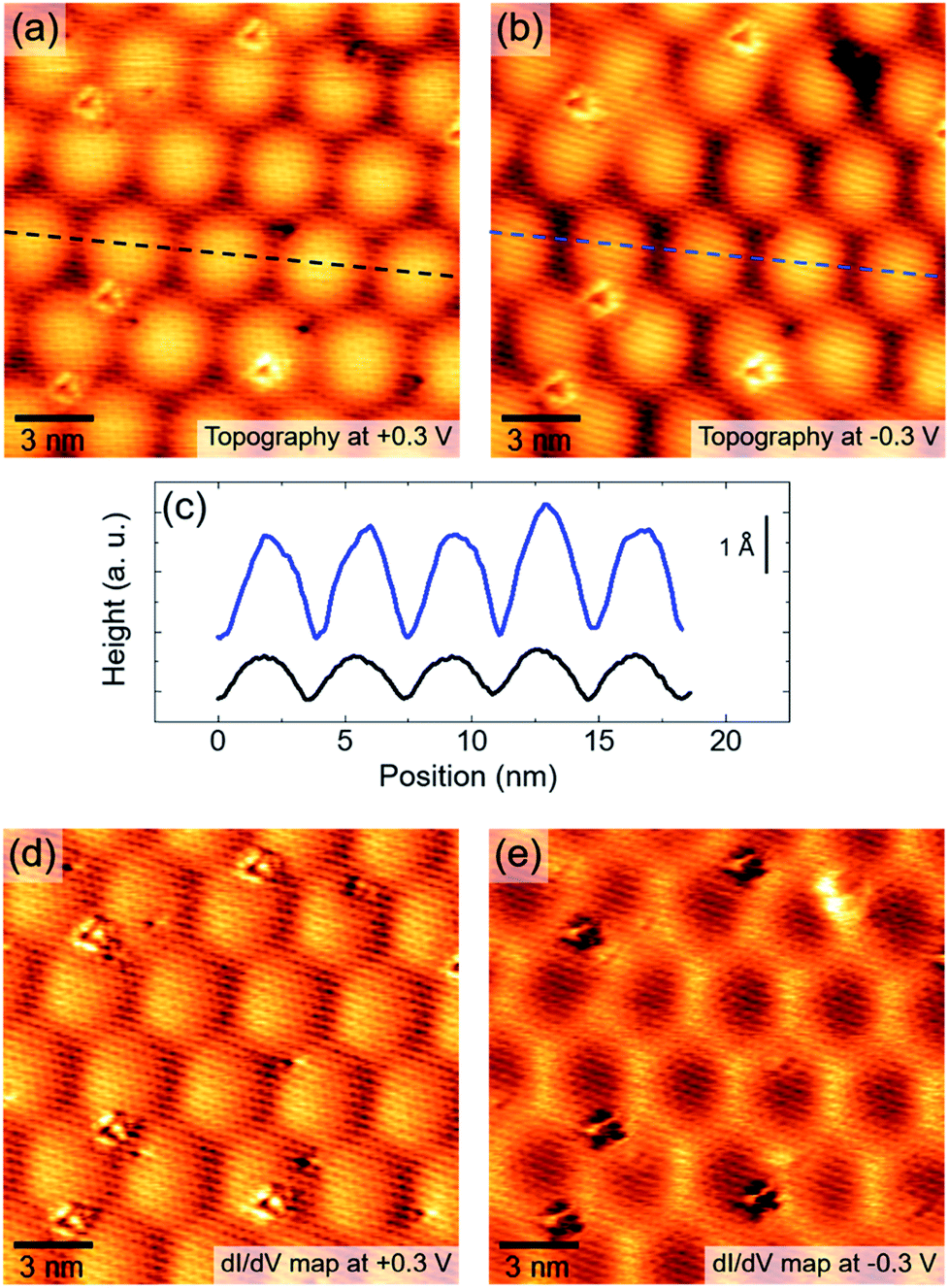 | ||
| Fig. 5 (a) and (b) Atomic resolution STM images taken at +0.3 V (a) and −0.3 V (b). (c) Topographic profiles: the black curve is taken along the black dashed line in (a), and the blue curve is taken along the blue dashed line in (b). (d) and (e) dI/dV maps corresponding to (a) and (b), respectively. | ||
The surface of MoS2 nanocrystals is also characterized by the presence of several point defects, as observed for example in the images of Fig. 5. We identified two kinds of defects, shown in the atomic resolution STM images of Fig. 6. In Fig. 6(a) the two different defects are labeled as D1 and D2: D1 looks like a single atomic vacancy, while D2 has a characteristic triangular shape and all D2 defects of the same nanocrystal are oriented in the same direction (see for example Fig. 5). The measured depths of D1 and D2 are 65 ± 5 pm and 45 ± 5 pm, respectively (Fig. 6(b)). We provide a possible interpretation of these defects based on the analysis of the atomic lattice arrangement revealed by high resolution STM images (Fig. 6(c) and (d)). Assuming that the brightest spots may be associated with surface S atoms, we argue that D1 defects (Fig. 6(c)) are consistent with monosulfur vacancies. This is in agreement with previously reported theoretical40 and experimental46 results on a 2H–MoS2(0001) surface. Different from D1, D2 defects involve more than one atomic site (Fig. 6(d)). Their peculiar triangular shape is consistent with a vacancy complex formed by one Mo and nearest S atoms. Noticeably, this interpretation agrees with the observation that in a single nanocrystal all D2 defects have the same orientation. We should note that our STM data can not unambiguously ascertain whether all six nearest S atoms or just the three surface ones are missing. However, the fact that the apparent depths of D1 and D2 are comparable suggests that only the three surface S sites are vacant, in addition to the Mo site. Interestingly, these two defects have, under stoichiometric conditions, the lowest calculated formation energy among various kinds of MoS2 point defects,47 further supporting our experimental observations and structural interpretation. Therefore, this investigation provides atomic-scale information on MoS2 surface defects, which have scarcely been explored by STM. This is essential to achieve a more complete understanding of their physical and chemical properties, which play a major role in functionalization48,49 of the MoS2 basal plane.
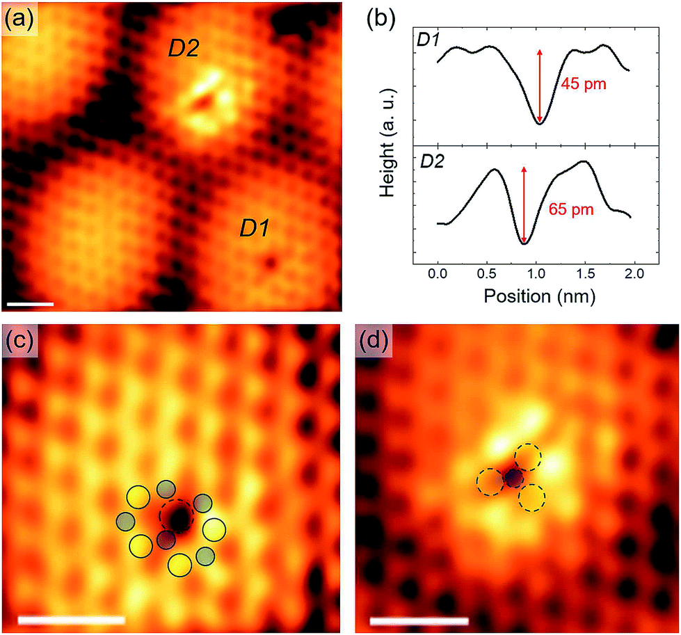 | ||
| Fig. 6 (a) Atomic resolution STM image showing two point defects of the MoS2 surface, labeled as D1 and D2 (V = 0.3 V, I = 1 nA). (b) Topographic profiles taken across D1 (upper panel) and D2 (lower panel) defects. (c) STM image of the D1 defect (V = 0.3 V, I = 1 nA). (d) STM image of the D2 defect (V = 0.3 V, I = 1 nA). The yellow and blue dots in (c) and (d) mark the positions of S and Mo atoms in the MoS2 lattice, respectively. Scale bars: 1 nm. | ||
The MoS2 nanocrystals growing at step edges or partially embedded in Au terraces form a peculiar lateral interface with Au, as revealed by the STM images in Fig. 7(a) and (b), which focus on the border region of the nanocrystals shown in Fig. 3(a) and (f). The in-plane MoS2–Au junction is usually imaged as a protruding region with an average width of 2 nm, running along the high symmetry directions of the moiré pattern. As shown by the plot in Fig. 7(c), the apparent height of the border, measured with respect to neighbouring Au, is ∼1 Å at a small bias and tends to decrease at higher (both positive and negative) voltages, suggesting a local metallic character of the in-plane junction. This observation agrees with the prediction of metallic edge MoS2–Au contact due to strong hybridization between Au and MoS2 edge states,14 a key property for the engineering of in-plane metal–semiconductor junctions with high charge injection efficiency.
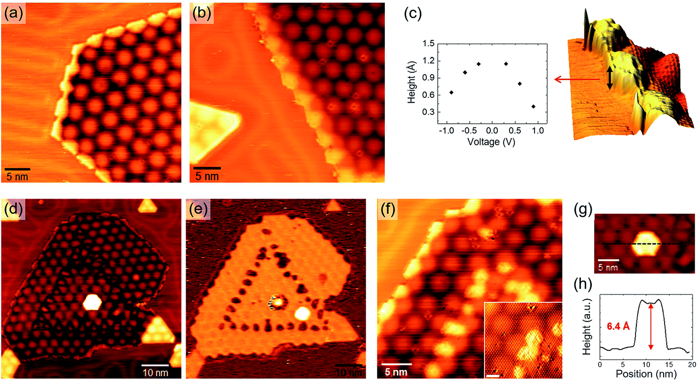 | ||
| Fig. 7 (a) and (b) STM images showing the lateral interface between Au and SL MoS2 nanocrystals. (c) Apparent height vs. voltage of the junction, measured with respect to neighbouring Au, as indicated in the 3D STM image on the right. (d) STM image of a partially embedded nanocrystal observed after the second growth cycle (V = 1.16 V, I = 0.35 nA). (e) dI/dV map corresponding to the STM image in (d). (f) Higher resolution STM image of the nanocrystal in (d) (V = 0.35 V, I = 0.5 nA). Inset: atomic resolution STM image (V = 0.3 V, I = 0.7 nA). Scale bar: 2 nm. (g) STM image of a 2nd layer MoS2 island. (h) Topographic profile along the black dashed line in (g). | ||
The partially embedded islands are also associated with a particular growth mechanism, observed as MoS2 coverage is increased after a second PLD + post-annealing process, identical to the first. Fig. 7(d) shows a partially embedded nanocrystal observed after the second growth cycle. We can notice that the moiré pattern is perturbed along a nearly triangular path, slightly visible on the nanocrystal surface. This is more evident in the corresponding dI/dV map (Fig. 7(e)), where small structures forming a triangle are imaged with the same contrast as the nanocrystal border. From higher resolution STM images (Fig. 7(f)), it is clear that the perimeter border and these protrusions share similar characteristics: they have the same apparent height at various bias voltages, suggesting a similar structure and LDOS. We can argue that these features formed the lateral junction between Au and a triangular partially embedded nanocrystal, produced with the first PLD + post-annealing cycle. Then, the second cycle makes the nanocrystal expand in a way that preserves some characteristic features of the original in-plane junction.
Incidentally, we observe the presence of a 2nd layer hexagonal MoS2 island atop the SL nanocrystal surface in Fig. 7(d) and (g). As shown by the line profile in Fig. 7(h), it has an apparent height of 6.4 Å with respect to the 1st layer, consistent with the 6.15 Å interlayer spacing of bulk MoS2.
3.3 Large-area single-layer MoS2
After having discussed the PLD synthesis and properties of SL MoS2 nanocrystals, we now discuss the growth of such structures into a continuous film, covering the gold surface almost completely. We explored two possible strategies for the synthesis of large-area SL MoS2. The first approach consists in repeating several times the same growth cycle, based on the PLD + post-annealing method introduced in the previous section. In the second, we address the possibility of optimizing PLD parameters to get a large-area SL MoS2 film with a single growth cycle.Starting with the first strategy, the STM images in Fig. 8 illustrate the sample morphology evolution as the same growth cycle is repeated up to five times. PLD and post-annealing parameters of the single growth cycle were tuned according to the experimental observations presented in the previous sections. In particular, the annealing temperature was set at 720 K to obtain well-defined SL MoS2 structures (Fig. 8(a)), without promoting the partial embedding mechanism, which would have made the STM surface analysis trickier, especially at higher coverage. As we have already shown (Fig. 1(e)), the first cycle produces isolated SL MoS2 nanocrystals of different sizes (Fig. 8(a)). Upon repeating the growth procedure on the same sample, MoS2 nanocrystals become larger (Fig. 8(b) and (c)). We note again the presence of brighter islands which are composed of SL nanocrystals on top of monoatomic high Au islands, according to topographic measurements. The formation of second layer MoS2 clusters can be observed after the 4th cycle (e.g. blue circles in Fig. 8(d) and (e)). After the 5th cycle, SL MoS2 covers about 90% of the substrate surface. The coverage increase, as a function of the cycle number, is approximately linear, as expected from layer-by-layer growth mode (Fig. 8(f)).
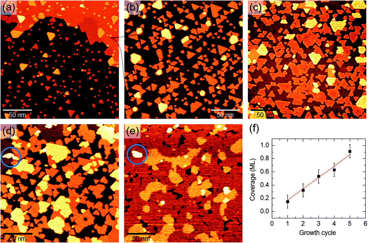 | ||
| Fig. 8 (a)–(e) 200 × 200 nm2 STM images of MoS2 on Au(111) taken after (a) one, (b) two, (c) three, (d) four and (e) five growth cycles. The single growth cycle is based on PLD (20 laser pulses) and post-annealing at 720 K. Measurement parameters: V = 1–1.7 V, I = 0.3–0.4 nA. The blue circles in (d) and (e) indicate 2nd layer MoS2 islands. (f) MoS2 coverage (expressed in ML) as a function of the number of growth cycles. The red line is a linear fit of experimental data. | ||
The second strategy is aimed at producing a SL MoS2 film in a one-step PLD process. The laser fluence was properly tuned up to 1.2 J cm−2, by reducing the laser spot on the target at constant pulse energy (100 mJ). This resulted in increasing the amount of deposited material per laser pulse. Then we optimized the number of laser pulses in order to get, after post-annealing at 720 K, the desired film morphology. The resulting sample, obtained with 30 laser pulses, is shown in Fig. 9. STM images (Fig. 9(a) and (b)) show MoS2 structures covering the gold surface almost completely. We estimated an average coverage of 0.92 ML from the analysis of several large-scale STM images. As verified by topographic measurements (inset of Fig. 9(b)), MoS2 forms a SL film, whose surface corrugation is modulated by the characteristic moiré pattern. Very few 2nd layer nanoclusters can be seen atop the SL surface (indicated by arrows in Fig. 9(a)). High resolution STM images reveal line defects on the MoS2 surface (Fig. 9(c)), which may be associated with 60° domain boundaries formed by merging of differently oriented crystals, as discussed in the previous section (Fig. 2).
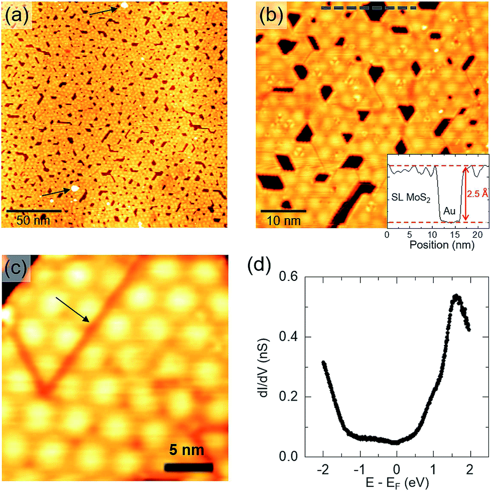 | ||
| Fig. 9 (a) 200 × 200 nm2 and (b) 100 × 100 nm2 STM images of SL MoS2 on Au(111) synthesized with a single growth cycle of PLD and post-annealing at 720 K (V = 1.9 V, I = 0.5 nA). The arrows in (a) indicate 2nd layer MoS2 clusters. Inset of (b): topographic profile along the grey dashed line. (c) High resolution STM image of the same film. The arrow indicates a boundary between differently oriented domains (V = 1.26 V, I = 0.35 nA). (d) STS spectrum of SL MoS2 on Au(111). | ||
STS measurements provided information on the electronic properties of the synthesized film. Point-spectroscopy differential conductivity (dI/dV) curves as a function of tip–sample voltage (V) were acquired at different points of the MoS2 surface, away from borders and domain boundaries, and then averaged to get a representative dI/dV curve. Such quantity, shown in Fig. 9(d), is proportional to the surface DOS, to a first approximation.50 We observe a semiconducting behavior with low DOS in a ∼2 eV wide energy range across the Fermi level (positioned at 0 eV). The onsets of valence and conduction bands occur approximately at −1.5 eV and 0.5 eV, respectively. These measurements agree well with the expected 1.9 eV optical band gap of SL MoS2 and previously reported STS measurements of MoS2 grown on Au substrates by means of other techniques.9 However, precise estimation of band onsets is difficult due to both thermal broadening, which affects spectral resolution, and the non-vanishing value of tunneling conductivity inside the gap region. The latter is indicative of a slight metalization of the film, as a result of sulfur-mediated interface hybridization with Au states.13,15,16 The MoS2–Au interaction is also responsible for the n-type character revealed by STS, which is due to Fermi level pinning near the conduction band onset, induced by interface charge redistribution.13–15
The observed strong interface coupling is expected to have a significant impact on the vibrational, electronic and optical properties of MoS2. A combination of Raman and photoluminescence (PL) spectroscopy is a valuable tool to investigate this aspect. We performed Raman and PL measurements ex situ under ambient conditions. After that, we put the sample back into the UHV chamber and observed it by STM, revealing that the surface morphology was not significantly affected by air exposure (not shown). This is a clear indication of the chemical stability of PLD-grown SL MoS2 at least upon few hours of air exposure. We report in Fig. 10(a) the Raman spectra of large-area SL MoS2 films synthesized with the two strategies described before, i.e. the multi-step and the one-step PLD processes. For comparison, we also report the spectrum acquired on a bulk crystalline MoS2 sample, which shows the two principal peaks of 2H–MoS2 at 382 cm−1 and 408 cm−1, associated with in-plane E12g and out-of-plane A1g vibrational modes, respectively.17 Both peaks are sharp, with a width of less than 4 cm−1, as expected for crystals. In the spectra of MoS2/Au(111) these two vibrational features are significantly modified: both peaks shift to lower frequencies, and, especially for the A1g mode, strong broadening and intensity attenuation are observed, resulting in an inversion of the intensity ratio between them. Numerical analysis based on Lorentzian fitting curves provides the data reported in Table 1. Different mechanisms due to the interaction with the Au substrate may contribute to modification of the vibrational modes, such as out-of-plane strain, which weakens the intralayer bond strength,15,51,52 and n-type doping.20 The latter, whose presence is confirmed by our STS measurements, is effective in softening and broadening the A1g peak due to its high sensitivity to electron–phonon coupling.20 The in-plane E12g vibrational mode is less sensitive to doping,20 but is strongly affected by strain effects.18,19 We note that our STM observations provide an average lattice parameter (3.18 ± 0.05 Å) comparable with the unstrained value. However, the lattice constant is measured from 2D FFTs of atomic resolution STM images, which, averaging over a relatively large number of unit cells, do not allow detection of small local variations. Therefore, we can not rule out the presence of local strain effects, for instance, those induced by the moiré superlattice. Indeed, it is reported for other 2D systems, such as graphene,53 that moiré patterns can influence the vibrational properties revealed by Raman spectra. Therefore, it is likely that the softening of the E12g mode is the result of a complex interplay of moiré-induced local strain and out-of-plane interaction with Au atoms. The data reported in Table 1 also evidence a larger variation of all the Raman parameters for the film synthesized with the one-step process with respect to the multi-step one, suggesting a stronger interaction with the Au substrate for this film. We may speculate that the multi-step process allows a relaxation of the interaction effects. An important parameter derived from Raman data is the frequency difference between A1g and E12g modes, usually used in the literature to assess the number of layers in ultrathin MoS2 flakes, as it decreases from about 25 cm−1 for bulk MoS2 down to about 18 cm−1 for a single layer.17 Our bulk value of 25.6 cm−1 is comparable with the one reported in the literature.17 On the other hand, the values we found for our SL MoS2 on Au(111) are larger than expected (about 23 cm−1), in comparison to both exfoliated21 and CVD-grown51,54 SL MoS2 on the Au substrate. This discrepancy can be ascribed to the simultaneous presence in our case of the two interface effects described above, n-type doping and strain, which influence the position of the two peaks in different ways. Hence, while STM provides unambiguous evidence for the single-layer structure of the film, Raman measurements cannot be directly correlated with MoS2 thickness due to the substrate influence on the peak shape, position and intensity of vibrational modes.
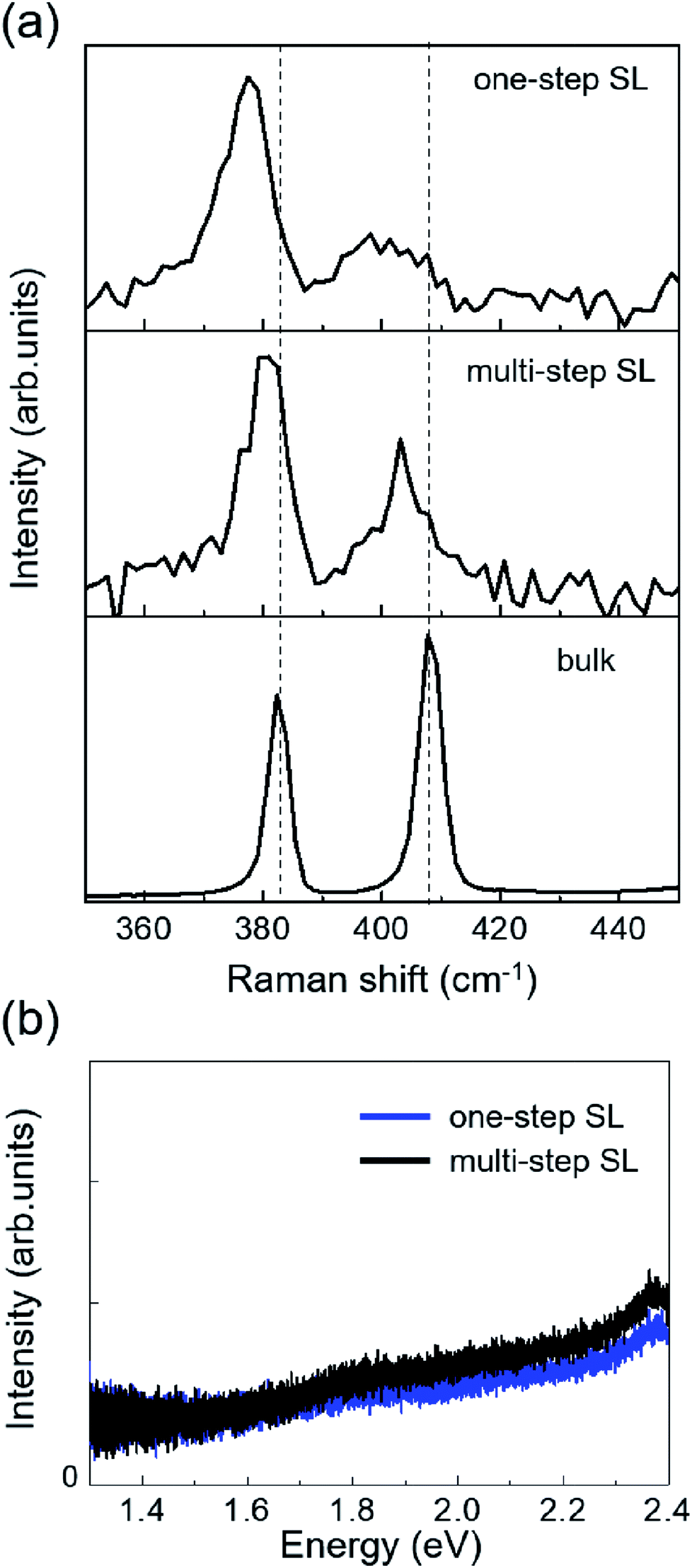 | ||
| Fig. 10 (a) Raman spectra of SL MoS2 on Au(111) (upper and central panels) and bulk MoS2 (lower panel). Vertical lines refer to expected bulk peak positions. (b) PL spectra of SL MoS2 films on Au(111) synthesized by multi-step (black) and single-step (blue) PLD processes. | ||
| E12g | A1g |
|
|
|||
|---|---|---|---|---|---|---|
| Position | Width | Position | Width | |||
| One-step SL | 377.1 | 9.1 | 400.9 | 13.4 | 23.8 | 0.45 |
| Multi-step SL | 382.6 | 3.6 | 408.2 | 3.9 | 25.6 | 1.456 |
| Bulk | 382.6 | 3.6 | 408.2 | 3.9 | 25.6 | 1.456 |
The interface interaction not only influences the vibrational properties of MoS2 films but also their electronic and optical ones, which can be investigated by means of photoluminescence (PL) spectroscopy. It is reported that SL MoS2 is a direct band gap semiconductor showing intense PL at 1.9 eV.2 Using a 514.5 nm excitation wavelength (corresponding to 2.41 eV) on our SL MoS2 films we obtained the spectra shown in Fig. 10(b). The PL spectra do not show the typical excitonic emission of SL MoS2, and the slight intensity rise at higher energies is solely due to the substrate. This total PL quenching is likely due to charge transfer with Au upon excitation, which prevents the excitonic recombination. This effect has also been observed in CVD-grown SL MoS2 on Au foil54 but not in exfoliated SL MoS2 on Au.21 Therefore, the PL quenching has to be related to the nature of the metal–semiconductor junction at the interface resulting from the synthesis process. Further study of this effect may highlight the role of growth mechanisms in determining the electronic and optical properties of MoS2/metal heterostructures.
In conclusion of this section, we point out that both our PLD growth strategies lead to the synthesis of large-area SL MoS2 films over the whole Au substrate (about 1 cm2). The film uniformity was verified by means of STM and Raman measurements in different regions of the sample (see the ESI†). Neither the large-scale STM images (Fig. S1†) nor the Raman spectra (Fig. S2†) revealed any difference from one sample region to another, thus guaranteeing the large-area uniformity of our SL MoS2 films. The two PLD growth approaches, i.e. multi-step vs. one-step, yield MoS2 films with similar surface properties, except for some minor morphological and structural differences. By comparing the large-scale STM images (e.g.Fig. 8(e) and 9(a)), it is found that the multi-step film is characterized by a larger fraction of 2nd layer MoS2 islands and mono-atomic high Au patches emerge; the latter is probably due to stress relaxation mechanisms and is not observed in the one-step film. These different characteristics are likely to influence the MoS2 vibrational properties, causing the larger down-shift of vibrational modes observed in the Raman spectrum of the one-step film (Fig. 10(a)).
4 Conclusions
We studied the surface properties of SL MoS2 deposited on Au(111) by PLD, starting from the growth of MoS2 nanocrystals to the formation of a SL film uniformly covering the substrate surface on the centimeter scale. Our measurements revealed the influence of MoS2–Au interaction on the structural, electronic and vibrational properties, such as rotational effects on the MoS2 lattice orientation and the modification of E12g and A1g vibrational modes. We also studied the formation of in-plane MoS2/Au heterojunctions and the atomic-scale structure of MoS2 point defects. This investigation provides insight into the interaction between Au and MoS2 at the 2D limit and sets the basis for studying 2D heterostructures between MoS2 and other metals, which is crucial for the design of contacts in MoS2-based devices.Our work also demonstrates how PLD, although not traditionally used for fundamental surface science, may effectively serve as a flexible technique to produce nanoscale systems as well as large-area device-oriented 2D films, while meeting high surface quality standards. Thanks to the PLD versatility, this experimental approach can be suitably applied to the study of more complex 2D systems (e.g. TMD alloys or 2D lateral/vertical heterostructures), with the possibility of investigating in situ the growth mechanisms and surface properties of the synthesized material.
Conflicts of interest
There are no conflicts to declare.Acknowledgements
F. Tumino, C. S. Casari, V. Russo and A. Li Bassi acknowledge funding from the European Research Council (ERC) under the European Union's Horizon 2020 research and innovation programme ERC – Consolidator Grant (ERC CoG 2016 EspLORE grant agreement no. 724610, website: http://www.esplore.polimi.it).References
- Q. H. Wang, K. Kalantar-Zadeh, A. Kis, J. N. Coleman and M. S. Strano, Electronics and optoelectronics of two-dimensional transition metal dichalcogenides, Nat. Nanotechnol., 2012, 7(11), 699–712 CrossRef CAS PubMed.
- K. F. Mak, C. Lee, J. Hone, J. Shan and T. F. Heinz, Atomically thin MoS2: a new direct-gap semiconductor, Phys. Rev. Lett., 2010, 105(13), 136805 CrossRef PubMed.
- A. Splendiani, L. Sun, Y. Zhang, T. Li, J. Kim, C.-Y. Chim, G. Galli and F. Wang, Emerging photoluminescence in monolayer MoS2, Nano Lett., 2010, 10(4), 1271–1275 CrossRef CAS PubMed.
- B. Radisavljevic, A. Radenovic, J. Brivio, I. V. Giacometti and A. Kis, Single-layer MoS2 transistors, Nat. Nanotechnol., 2011, 6(3), 147–150 CrossRef CAS PubMed.
- R. R. Chianelli, M. H. Siadati, M. P. De la Rosa, G. Berhault, J. P. Wilcoxon, R. Bearden Jr and B. L. Abrams, Catalytic properties of single layers of transition metal sulfide catalytic materials, Catal. Rev., 2006, 48(1), 1–41 CrossRef CAS.
- X. Zou and Y. Zhang, Noble metal-free hydrogen evolution catalysts for water splitting, Chem. Soc. Rev., 2015, 44(15), 5148–5180 RSC.
- S. Helveg, J. V. Lauritsen, E. Lægsgaard, I. Stensgaard, J. K. Nørskov, B. S. Clausen, H. Topsøe and F. Besenbacher, Atomic-scale structure of single-layer MoS2 nanoclusters, Phys. Rev. Lett., 2000, 84(5), 951 CrossRef CAS PubMed.
- T. F. Jaramillo, K. P. Jörgensen, J. Bonde, J. H. Nielsen, S. Horch and I. Chorkendorff, Identification of active edge sites for electrochemical H2 evolution from MoS2 nanocatalysts, Science, 2007, 317(5834), 100–102 CrossRef CAS PubMed.
- S. G. Sørensen, H. G. Füchtbauer, A. K. Tuxen, A. S. Walton and J. V. Lauritsen, Structure and electronic properties of in situ synthesized single-layer MoS2 on a gold surface, ACS Nano, 2014, 8(7), 6788–6796 CrossRef PubMed.
- N. Salazar, I. Beinik and J. V. Lauritsen, Single-layer MoS2 formation by sulfidation of molybdenum oxides in different oxidation states on Au(111), Phys. Chem. Chem. Phys., 2017, 19(21), 14020–14029 RSC.
- J. Hall, B. Pielić, C. Murray, W. Jolie, W. Tobias, C. Busse, M. Kralj and T. Michely, Molecular beam epitaxy of quasi-freestanding transition metal disulphide monolayers on van der Waals substrates: a growth study, 2D Mater., 2018, 5(2), 025005 CrossRef.
- H. Bana, E. Travaglia, L. Bignardi, P. Lacovig, C. E. Sanders, M. Dendzik, M. Michiardi, M. Bianchi, D. Lizzit and F. Presel, et al., Epitaxial growth of single-orientation high-quality MoS2 monolayers, 2D Mater., 2018, 5(3), 035012 CrossRef.
- I. Popov, G. Seifert and D. Tománek, Designing electrical contacts to MoS2 monolayers: a computational study, Phys. Rev. Lett., 2012, 108(15), 156802 CrossRef PubMed.
- J. Kang, W. Liu, D. Sarkar, D. Jena and K. Banerjee, Computational study of metal contacts to monolayer transition-metal dichalcogenide semiconductors, Phys. Rev. X, 2014, 4(3), 031005 Search PubMed.
- C. Gong, L. Colombo, R. M. Wallace and K. Cho, The unusual mechanism of partial fermi level pinning at metal–MoS2 interfaces, Nano Lett., 2014, 14(4), 1714–1720 CrossRef CAS PubMed.
- A. Bruix, J. A. Miwa, N. Hauptmann, D. Wegner, S. Ulstrup, S. S. Grønborg, C. E. Sanders, M. Dendzik, A. G. Čabo and M. Bianchi, et al., Single-layer MoS2 on Au(111): Band gap renormalization and substrate interaction, Phys. Rev. B: Condens. Matter Mater. Phys., 2016, 93(16), 165422 CrossRef.
- C. Lee, H. Yan, L. E. Brus, T. F. Heinz, J. Hone and S. Ryu, Anomalous lattice vibrations of single-and few-layer MoS2, ACS Nano, 2010, 4(5), 2695–2700 CrossRef CAS PubMed.
- H. J. Conley, B. Wang, J. I. Ziegler, R. F. Haglund Jr, S. T. Pantelides and K. I. Bolotin, Bandgap engineering of strained monolayer and bilayer MoS2, Nano Lett., 2013, 13(8), 3626–3630 CrossRef CAS PubMed.
- C. Rice, R. J. Young, R. Zan, U. Bangert, D. Wolverson, T. Georgiou, R. Jalil and K. S. Novoselov, Raman-scattering measurements and first-principles calculations of strain-induced phonon shifts in monolayer MoS2, Phys. Rev. B: Condens. Matter Mater. Phys., 2013, 87(8), 081307 CrossRef.
- B. Chakraborty, A. Bera, D. V. S. Muthu, S. Bhowmick, U. V. Waghmare and A. K. Sood, Symmetry-dependent phonon renormalization in monolayer MoS2 transistor, Phys. Rev. B: Condens. Matter Mater. Phys., 2012, 85(16), 161403 CrossRef.
- M. Buscema, G. A. Steele, H. S. J. van der Zant and A. Castellanos-Gomez, The effect of the substrate on the raman and photoluminescence emission of single-layer MoS2, Nano Res., 2014, 7(4), 561–571 CrossRef.
- T. A. J. Loh and D. H. C. Chua, Growth mechanism of pulsed laser fabricated few-layer MoS2 on metal substrates, ACS Appl. Mater. Interfaces, 2014, 6(18), 15966–15971 CrossRef CAS PubMed.
- I. S. Martha, S. H. Yoo, S. Moreno, X. Yang, J. P. Oviedo, H. Choi, H. N. Alshareef, M. J. Kim, M. Minary-Jolandan and M. A. Quevedo-Lopez, Large-area deposition of MoS2 by pulsed laser deposition with in situ thickness control, ACS Nano, 2016, 10(6), 6054–6061 CrossRef PubMed.
- C. R. Serrao, A. M. Diamond, S.-L. Hsu, L. You, S. Gadgil, J. Clarkson, C. Carraro, R. Maboudian, C. Hu and S. Salahuddin, Highly crystalline MoS2 thin films grown by pulsed laser deposition, Appl. Phys. Lett., 2015, 106(5), 052101 CrossRef.
- G. Siegel, Y. P. Venkata Subbaiah, M. C. Prestgard and A. Tiwari, Growth of centimeter-scale atomically thin MoS2 films by pulsed laser deposition, APL Mater., 2015, 3(5), 056103 CrossRef.
- T. A. J. Loh, D. H. C. Chua and A. T. S. Wee, One-Step Synthesis of Few-Layer WS2 by Pulsed Laser Deposition, Sci. Rep., 2015, 5, 18116 CrossRef CAS PubMed.
- M. Mahjouri-Samani, M. Tian, K. Wang, A. Boulesbaa, C. M. Rouleau, A. A. Puretzky, M. A. McGuire, B. R. Srijanto, K. Xiao and G. Eres, et al., Digital transfer growth of patterned 2d metal chalcogenides by confined nanoparticle evaporation, ACS Nano, 2014, 8(11), 11567–11575 CrossRef CAS PubMed.
- M. Mahjouri-Samani, G. Ryan, M. Tian, K. Wang, A. A. Puretzky, C. M. Rouleau, G. Eres, I. N. Ivanov, K. Xiao and M. A. McGuire, et al., Pulsed laser deposition of photoresponsive two-dimensional GaSe nanosheet networks, Adv. Funct. Mater., 2014, 24(40), 6365–6371 CrossRef CAS.
- F. Tumino, C. S. Casari, M. Passoni, C. E. Bottani and A. Li Bassi, Pulsed laser deposition of two-dimensional ZnO nanocrystals on Au(111): growth, surface structure and electronic properties, Nanotechnology, 2016, 27(47), 475703 CrossRef CAS PubMed.
- S. S. Grønborg, S. Ulstrup, M. Bianchi, M. Dendzik, C. E. Sanders, J. V. Lauritsen, P. Hofmann and J. A. Miwa, Synthesis of epitaxial single-layer MoS2 on Au(111), Langmuir, 2015, 31(35), 9700–9706 CrossRef PubMed.
- J. V. Barth, H. Brune, G. Ertl and R. J. Behm, Scanning Tunneling Microscopy Observations on the Reconstructed Au(111) Surface: Atomic Structure, Long-Range Superstructure, Rotational Domains, and Surface Defects, Phys. Rev. B: Condens. Matter Mater. Phys., 1990, 42(15), 9307 CrossRef CAS.
- Ch. Wöll, S. Chiang, R. J. Wilson and P. H. Lippel, Determination of Atom Positions at Stacking-Fault Dislocations on Au(111) by Scanning Tunneling Microscopy, Phys. Rev. B: Condens. Matter Mater. Phys., 1989, 39, 7988–7991 CrossRef.
- C. S. Casari, S. Foglio, F. Siviero, A. Li Bassi, M. Passoni and C. E. Bottani, Direct observation of the basic mechanisms of pd island nucleation on Au(111), Phys. Rev. B: Condens. Matter Mater. Phys., 2009, 79(19), 195402 CrossRef.
- D. Nečas and P. Klapetek, Gwyddion: an Open-Source Software for SPM Data Analysis, Open Phys., 2012, 10(1), 181–188 Search PubMed.
- Jl A. Wilson and A. D. Yoffe, The transition metal dichalcogenides discussion and interpretation of the observed optical, electrical and structural properties, Adv. Phys., 1969, 18(73), 193–335 CrossRef CAS.
- P. A. Young, Lattice parameter measurements on molybdenum disulphide, J. Phys. D: Appl. Phys., 1968, 1(7), 936 CrossRef.
- X. Liu, I. Balla, H. Bergeron, G. P. Campbell, M. J. Bedzyk and M. C. Hersam, Rotationally commensurate growth of MoS2 on epitaxial graphene, ACS Nano, 2015, 10(1), 1067–1075 CrossRef PubMed.
- C. Zhang, A. Johnson, C.-L. Hsu, L.-J. Li and C.-K. Shih, Direct imaging of band profile in single layer MoS2 on graphite: quasiparticle energy gap, metallic edge states, and edge band bending, Nano Lett., 2014, 14(5), 2443–2447 CrossRef CAS PubMed.
- K. Kobayashi and J. Yamauchi, Electronic structure and scanning-tunneling-microscopy image of molybdenum dichalcogenide surfaces, Phys. Rev. B: Condens. Matter Mater. Phys., 1995, 51(23), 17085 CrossRef CAS.
- J. D. Fuhr, A. Saúl and J. O. Sofo, Scanning tunneling microscopy chemical signature of point defects on the MoS2(0001) surface, Phys. Rev. Lett., 2004, 92(2), 026802 CrossRef PubMed.
- A. Altibelli, C. Joachim and P. Sautet, Interpretation of STM images: The MoS2 surface, Surf. Sci., 1996, 367(2), 209–220 CrossRef CAS.
- E. Perrot, A. Humbert, A. Piednoir, C. Chapon and C. R. Henry, STM and TEM studies of a model catalyst: Pd/MoS2(0001), Surf. Sci., 2000, 445(2–3), 407–419 CrossRef CAS.
- M. V. Bollinger, J. V. Lauritsen, K. W. Jacobsen, J. K. Nørskov, S. Helveg and F. Besenbacher, One-dimensional metallic edge states in MoS2, Phys. Rev. Lett., 2001, 87(19), 196803 CrossRef CAS PubMed.
- M. V. Bollinger, K. W. Jacobsen and J. K. Nørskov, Atomic and electronic structure of MoS2 nanoparticles, Phys. Rev. B: Condens. Matter Mater. Phys., 2003, 67(8), 085410 CrossRef.
- K. Hermann, Periodic overlayers and moiré patterns: Theoretical studies of geometric properties, J. Phys.: Condens. Matter, 2012, 24(31), 314210 CrossRef PubMed.
- R. Addou, L. Colombo and R. M. Wallace, Surface defects on natural MoS2, ACS Appl. Mater. Interfaces, 2015, 7(22), 11921–11929 CrossRef CAS PubMed.
- Z. Wu, X. Zou, S. Najmaei, L. Zheng, Y. Shi, J. Kong, J. Lou, P. M. Ajayan, B. I. Yakobson and J.-C. Idrobo, Intrinsic structural defects in monolayer molybdenum disulfide, Nano Lett., 2013, 13(6), 2615–2622 CrossRef PubMed.
- L. Hong, C. Tsai, A. L. Koh, L. Cai, A. W. Contryman, A. H. Fragapane, J. Zhao, H. S. Han, H. C. Manoharan and F. Abild-Pedersen, et al., Activating and optimizing MoS2 basal planes for hydrogen evolution through the formation of strained sulphur vacancies, Nat. Mater., 2016, 15(1), 48 CrossRef PubMed.
- D. Le, T. B. Rawal and T. S. Rahman, Single-layer MoS2 with sulfur vacancies: structure and catalytic application, J. Phys. Chem. C, 2014, 118(10), 5346–5351 CrossRef CAS.
- M. Passoni, F. Donati, A. Li Bassi, C. S. Casari and C. E. Bottani, Recovery of local density of states using scanning tunneling spectroscopy, Phys. Rev. B: Condens. Matter Mater. Phys., 2009, 79(4), 045404 CrossRef.
- S. Yasuda, R. Takahashi, R. Osaka, R. Kumagai, Y. Miyata, S. Okada, Y. Hayamizu and K. Murakoshi, Out-of-plane strain induced in a moiré superstructure of monolayer MoS2 and MoSe2 on Au(111), Small, 2017, 13(31), 1700748 CrossRef PubMed.
- M. Pena-Alvarez, E. del Corro, Á. Morales-García, L. Kavan, M. Kalbac and O. Frank, Single layer molybdenum disulfide under direct out-of-plane compression: low-stress band-gap engineering, Nano Lett., 2015, 15(5), 3139–3146 CrossRef PubMed.
- A. Eckmann, J. Park, H. Yang, D. Elias, A. S. Mayorov, G. Yu, R. Jalil, K. S. Novoselov, R. V. Gorbachev and M. Lazzeri, et al., Raman fingerprint of aligned graphene/h-bn superlattices, Nano Lett., 2013, 13(11), 5242–5246 CrossRef CAS PubMed.
- J. Shi, D. Ma, G.-F. Han, Y. Zhang, Q. Ji, T. Gao, J. Sun, X. Song, C. Li and Y. Zhang, et al., Controllable growth and transfer of monolayer MoS2 on Au foils and its potential application in hydrogen evolution reaction, ACS Nano, 2014, 8(10), 10196–10204 CrossRef CAS PubMed.
Footnote |
| † Electronic supplementary information (ESI) available. See DOI: 10.1039/c8na00126j |
| This journal is © The Royal Society of Chemistry 2019 |