
 Open Access Article
 This Open Access Article is licensed under a Creative Commons Attribution-Non Commercial 3.0 Unported Licence
Pulsed-grown graphene for flexible transparent conductors†
Pramoda K.
Nayak
 *
*
Department of Physics, Indian Institute of Technology Madras, Chennai 600036, India. E-mail: pnayak@iitm.ac.in
First published on 2nd January 2019
Abstract
In the race to find novel transparent conductors for next-generation optoelectronic devices, graphene is supposed to be one of the leading candidates, as it has the potential to satisfy all future requirements. However, the use of graphene as a truly transparent conductor remains a great challenge because its lowest sheet resistance demonstrated so far exceeds that of the commercially available indium tin oxide. The possible cause of low conductivity lies in its intrinsic growth process, which requires further exploration. In this work, I have approached this problem by controlling graphene nucleation during the chemical vapor deposition process as well as by adopting three distinct procedures, including bis(trifluoromethanesulfonyl)amide doping, post annealing, and flattening of graphene films. Additionally, van der Waals stacked graphene layers have been prepared to reduce the sheet resistance effectively. I have demonstrated an efficient and flexible transparent conductor with the extremely low sheet resistance of 40 Ω sq−1, high transparency (Tr ∼90%), and high mechanical flexibility, making it suitable for electrode materials in future optoelectronic devices.
Introduction
The next-generation optoelectronic devices require materials with high mechanical flexibility, light weight, and high electrical conductivity and optical transparency to be used as electrodes.1–4 Indium tin oxide (ITO) has been the most widely used transparent conductor in optoelectronic applications for over almost four decades. The sheet resistance (Rs) of ITO is thickness dependent and is found to be in the range of 5–60 Ω sq−1, with the transmittance (Tr) of about 85–90% for 40–870 nm film thickness,5 making it suitable for device applications. However, several drawbacks of ITO include the increased material cost, material deterioration due to ion diffusion, and brittleness, which limit its use in future flexible devices.6,7 On the other hand, graphene is optically transparent, i.e., each graphene layer has a very low opacity of 2.3%,6,8 it is flexible6,9 and it has high oxidation resistance,10,11 making it an ideal candidate for transparent conducting films (TCFs).12–15 Despite graphene's superior optical properties, flexibility, and relatively low manufacturing cost, the conductance of graphene sheets remains well below that of commercial ITO films.16Significant efforts have been made so far to reduce the Rs of graphene film by chemical doping,17–19 substitutional doping,20–22 or stacking of graphene films7,23,24 in parallel while maintaining a high Tr to improve its potential to be harnessed in optoelectronic applications. Although chemical doping has been shown to effectively reduce the Rs of graphene down to 150 Ω sq−1 at Tr = 87%,12 125 Ω sq−1 at Tr = 97.4%,13 and 80 Ω sq−1 at Tr = 80% for eight-layer stacked graphene,7 the adsorption of moisture, other atoms, and molecules onto graphene after chemical treatment leads to the increase of Rs within few days.25,26 Similarly, substitutional doping induces disorder in the graphene, thereby reducing its mobility as a result of scattering of Dirac electrons.27,28 Additionally, most doping processes decrease the optical transparency of graphene film by changing its band structure or by forming optically reflective nanoparticles at the surface,29,30 making it unsuitable for optoelectronic applications. Recently, a new growth technique has been introduced by Han et al.31 which involves cyclic injection of carbon precursor (CH4) during chemical vapor deposition (CVD) to suppress the multilayer patches generally formed using continuous CH4 flow, thereby improving both the optical and electrical performance of graphene. Similarly, other approaches, such as trifluoromethanesulfonimide (TFSA) doping,19,32–34 post annealing,35,36 and flattening of graphene films37 have been carried out to reduce the Rs of graphene. However, no systematic study exists so far that combines all the aforementioned approaches, which is highly desired to achieve superior graphene film suitable for the transparent conducting electrode.
In the present work, I have prepared a high-quality graphene film using pulsed-grown technique and investigated its optical and electrical performance using the combined effects of TFSA doping, stacking, post annealing and flattening. The prepared graphene film shows Rs of a few hundred Ω sq−1, on/off ratio of ∼13, along with a high I2D/IG ratio (>1.5). TFSA doped four layer stacked graphene films show a low Rs of 40 Ω sq−1 and transmittance of 90%, which are almost comparable to those of ITO. The combination of TFSA doping, post annealing and flattening of graphene film is found to reduce the Rs by 80%, the highest value reported so far. Finally, the mechanical flexibility of this highly conducting and transparent film has been demonstrated, making it suitable for application as a flexible transparent conducting electrode.
Results and discussion
Growth of monolayer graphene on Cu substrate using CVD has been a well-established technique since 2009,38–40 where the nucleation and growth of graphene usually occurs by exposure of the Cu surface to a hydrocarbon gas under atmospheric pressure, low pressure or ultra-high vacuum (UHV) conditions. However, the grain boundaries in such graphene films act as scattering centers for electron waves, limiting electron mobility.41,42 To minimize the grain boundary effect, I have modified the graphene growth process by supplying CH4 in short pulses31 instead of the conventional continuous CH4 flow during the CVD growth of graphene on Cu, as illustrated in Fig. 1. The details of the synthesis process are provided in Fig. S1 (see ESI†). In the case of continuous CH4 flow used in literature so far, the rate of nucleation is very high, which leads to high density of graphene nucleation seeds over the Cu surface.43–47 These nucleation seeds interfere each other when growth persists, and hence, the graphene domains do not grow in the preferred orientation, and the average graphene domain size shrinks. On the other hand, in the pulsed-grown method, graphene domains are seen to coalesce in a preferred direction to form larger islands of ∼100 μm size (shown by arrows in Fig. S2 of ESI†). This provides evidence that the nucleation rate is expected to be slow in the pulsed-grown method, which leads to low density of graphene nucleation seeds. It can be noted that the preliminary annealing of the Cu substrate leads to a reconstruction of atomic distribution over the surface,48 which causes directional growth of graphene domains, but not coalescence. As the Cu substrates used in this work were not pre-annealed, the directional growth due to substrate effect can be ruled out.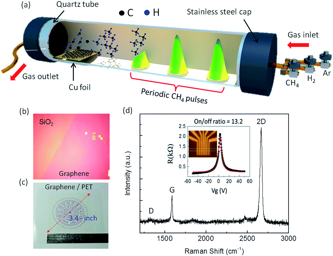 | ||
| Fig. 1 (a) Schematic of the designed CVD system with introduction of periodic CH4 pulses into the reaction zone. (b) OM image of pulse-grown graphene film transferred onto marked 300 nm SiO2/Si substrate. The graphene film is clearly distinguishable from bare SiO2 with the color contrast. (c) Camera image of 3.4-inch graphene film transferred onto 125 μm thick PET substrate. (d) Raman spectrum of transferred graphene film on SiO2 substrate. Both G and 2D band peaks are very symmetric with full width at half maximum (FWHM) of 15 and 30 cm−1, respectively. The I2D/IG intensity ratio is >1.5, which confirms that the prepared graphene is monolayer. A slight D band intensity is present in the Raman spectrum, which probably arises from the etching process. The inset shows the R vs. Vg plot for graphene-based FET in back-gate configuration. | ||
In addition to lower nucleation rate, the purpose of the pulsed CH4 gas is to suppress carbon segregation at the defect sites in Cu, which aids in removing the multilayer patches generally formed using continuous CH4 flow.43 Moreover, the restoration time after each CH4 pulse increases the catalytic activity of H2 gas, during which hydrogen etches off the amorphous carbon atoms and the sp3 carbon network present on the surface. Repeated alternating cycles of growth with CH4 pulse and restoration of H2 treatment promote the complete transformation of the carbon chain to a most stable sp2 C–C network, as shown in Fig. S3 (ESI†). These hydrogen atoms not only promote the activation of physisorbed methane but also remove defects in carbon structures, which can be described in the following equation,
| Hs + (graphene-defects) ⇔ (graphene–C) + (CHx)s | (1) |
As a consequence, structural defects such as pentagon and heptagon structures are minimized, leading to a clean and defect-free graphene surface. The schematic illustration in Fig. S3a (see ESI†) shows the evolution of surface defects emerging from unexpected bumps, protrusions, and grooves on the surface; those bring up electron scattering issues in graphene, leading to Fermi velocity degradation. The dwell time of CH4 pulses also affects graphene domain size, as shown in Fig. S2.† Longer dwell time of CH4 pulses leads to a smaller graphene domain size of ∼2–3 μm (Fig. S2a and b†), whereas larger domain sizes of ∼20–30 μm could be achieved for shorter dwell time of CH4 pulses, as shown in Fig. S2c and d.† The preferred orientations of graphene domains are marked with arrows in Fig. S2,† where these domains are merged together to form larger islands (∼100 μm). The large graphene domain size along with the defect-free surface increases the mobility of the electrons, due to the low defect density and grain boundary effect,31 thereby decreasing the Rs. The as-prepared graphene film was transferred onto 300 nm SiO2/Si substrate using the conventional poly(methyl methacrylate) (PMMA)-based transfer process, as shown in Fig. S4 (see ESI†), similar to Lin et al.,49 and the optical microscope (OM) image is shown in Fig. 1b. For electromechanical characterization, the graphene film was also transferred onto a flexible polyethylene terephthalate (PET) substrate, and the corresponding OM image is shown in Fig. 1c. The quality of our graphene film is reflected from the symmetric 2D peak, large I2D/IG ratio (>1.5) and absence of D peak measured from the Raman spectrum on SiO2/Si substrate, as shown in Fig. 1d, which confirm that the prepared graphene is predominantly monolayer and defect free. Moreover, the R vs. Vg plot of the graphene-based field effect transistor (FET), shown inset in Fig. 1d, shows strong electron-hole symmetry, a narrow profile width (∼5.5 V), and gate modulation (on/off ratio) of about 13.2, which are the characteristic features of high-quality graphene.50,51
Several methods have been perused in order to reduce the Rs of graphene, including doping with TFSA, post annealing, flattening and stacking of graphene films. The schematics of the above processes are mentioned in Fig. S5 (see ESI†), and the overall processes are summarized below.
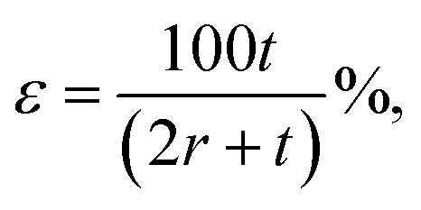
The organic dopant TFSA is hydrophobic in nature and an excellent candidate for doping graphene due to its following advantages: effective electron-withdrawing ability, high transmittance, smooth surface, and superior environmental stability.33 TFSA has been used as a p-type dopant in carbon nanotubes52 and also in graphene.19,33,34,53 TFSA, with a –NH group, easily loses a proton and transforms to TFSI upon accepting an electron from graphene, which is characteristic of a Brønsted acid.54 When an electron is transferred from graphene to TFSA, a charge–transfer complex is formed according to eqn (2),
| (CF3SO2)2NH + Graphene → [(CF3SO2)2N]− + H+ + Graphene+ | (2) |
Thus, there is hole doping in the graphene that results in a shift of the Fermi level. In order to visualize this doping effect, I have performed electronic band structure calculation of TFSA-doped graphene using density functional theory (DFT), and the results are displayed in Fig. 2a and b. The details of DFT calculation are mentioned in the method section. Fig. 2a shows the optimized position of TFSA molecules absorbed on the surface of monolayer graphene. The constituent atoms of TFSA, such as N, S, O, C and F are marked in blue, yellow, red, grey and green, respectively. From the band structure result (Fig. 2b), the band gap value was found to be almost zero; i.e., the gap between conduction band minimum (CBM) and valence band maximum (VBM) at the high-symmetry K point of the Brillouin zone and the Fermi level shifts below VBM, which is characteristic of p-doped graphene.55,56 TFSA-doped graphene was prepared by spinning a few droplets of TFSA over graphene film at 3000 rpm for 30 s. The Raman spectra of pure and TFSA-doped graphene are shown in Fig. 2c. The characteristic Raman peaks for pristine graphene, located at 1588 cm−1 and 2669 cm−1, correspond to G band (first-order Raman process) and 2D band (second-order Raman process), respectively.57 Both pristine and TFSA-doped graphene exhibit very intense and symmetric 2D peaks with a large I2D/IG ratio (>1.5). Compared to pristine graphene, doped graphene shows a large blue shift for both G peak (ΔG = 6 cm−1) and 2D peak (Δ2D = 33 cm−1), which confirms that there is charge transfer from graphene to TFSA, thereby causing p-doping,58 which coincides with my calculation result. Interestingly, the D-peak, which corresponds to the TO phonons around the K point of the Brillouin zone and is the signature of defects on the graphene surface, is found to be absent before or after doping. This observation indicates that TFSA treatment is not destructive to the chemical bonds of graphene, which is quite similar to HNO3-doped graphene.18
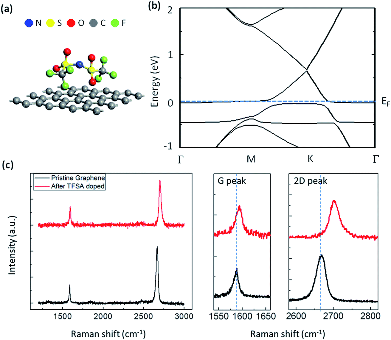 | ||
| Fig. 2 Effect of TFSA doping on the Raman spectra of pulsed-grown graphene. (a) Optimized position of TFSA molecules absorbed on the surface of monolayer graphene. The constituent atoms of TFSA, such as N, S, O, C and F are marked in blue, yellow, red, grey and green, respectively. (b) Band structure calculation of TFSA-doped graphene using DFT. The band gap is almost zero; i.e., the gap between conduction band minimum and valence band maximum at the high symmetry K point of the Brillouin zone and the Fermi level shifts below VBM due to p-doping. (c) Raman spectra of CVD graphene before and after TFSA doping. The G and 2D peaks of both the graphene films are extrapolated and plotted in separate panels for comparison. Compared to pristine graphene, doped graphene shows a large blue shift for both G peak (ΔG = 6 cm−1) and 2D peak (Δ2D = 33 cm−1), which confirms that there is charge transfer from graphene to TFSA. | ||
In the pursuit of transparent conducting applications, the optical and electrical properties of 1 × 1 cm2 pristine and doped graphene films prepared by pulsed-grown method were analyzed, as shown in Fig. 3. The optical transmittance of the graphene films in the visible range was measured using an UV-VIS-NIR spectrophotometer (UV-3600, Shimadzu). For this measurement, graphene films were transferred on a cover glass as a single layer and as multiple stacked layers, and a bare cover glass was used as a reference. Multiple-layered “graphene stacks” were created using the transfer process sequentially. Fig. 3a depicts the wavelength dependence of the optical transparency of one- to four-layer-stacked pristine graphene films. The transmittance, Tr (%), of stacked graphene films at λ = 550 nm extracted from (a) was found to be 97.3, 94.6, 92.9 and 90 for one, two, three and four layers, respectively (Fig. 3b). Because each graphene layer has an opacity of 2.3%,8 the transmittance decreases by ∼2.3% for each added layer, indicating that the film behaves as a set of individual graphene layers.8,59 A slight variation in the transmittance values as per layer numbers predicted from theoretical calculation may be due to impurities present in the interface of the artificially built weak van der Waals stacked layers.60 Similar behavior has also been observed by Karsy et al.7 for stacked graphene layers. The evolution of graphene layers is also detectable from the change in color contrast observed from the optical images, as shown in the inset of Fig. 3b, which is minimum for one layer and maximum for four layers. The optical transmittance of TFSA-doped graphene also varies in a similar fashion to pristine graphene. For comparison, the optical transmittance of pristine and doped monolayer graphene is shown in Fig. 3c. It is observed that the Tr values of both films at λ = 550 nm are almost same, and hence, TFSA doping has no effect on the Tr of the graphene film. Fig. 3d shows the Rs of pristine and doped graphene films measured using van der Pauw method. The details of Rs measurement of graphene films are shown in Fig. S6 (see ESI†). In both the cases, Rs decreases with the increase in number of graphene layers. The Rs of monolayer graphene film is 288 Ω sq−1 with Tr of 97.3%, whereas that of four-layer graphene is 86 Ω sq−1, while still maintaining a relatively high Tr of about 90%. Similarly, the Rs of doped graphene varies from 134 Ω sq−1 to a lowest value of 40 Ω sq−1 with the increase in number of graphene layers from one to four, while maintaining the same Tr values as those of pure graphene layers. In principle, the Rs of multilayer film, Rsn, is related to the Rs of one layer film, Rs1, by the relation Rsn = Rs1/n, where n is the number of graphene layers if all layers are acting independently of each other. However, the average Rs of our films decreases slightly by stacking four graphene layers. The discrepancy might be explained by considering that the cracks in one film are bridged by its neighboring films, thus increasing the conductivity.61 As stated earlier, when an electron is transferred from the graphene to TFSA, graphene becomes p-doped according to eqn (2). This results in a shift of the Fermi level (Fig. 3b), which increases the carrier concentration and thus the conductivity of the graphene layers. With the increase in layer numbers, there is further increment in the carrier concentration and density of states (DOS) at the Dirac point, which results in higher conductivity. This effect was first observed with single-walled carbon nanotubes (SWCNTs), where the doping of the SWCNTs with TFSA led to an increase in the conductivity of SWCNT films.52 Since SWCNTs and graphene have essentially the same chemical structure, it is worth noting that TFSA doping yields lower sheet resistance.
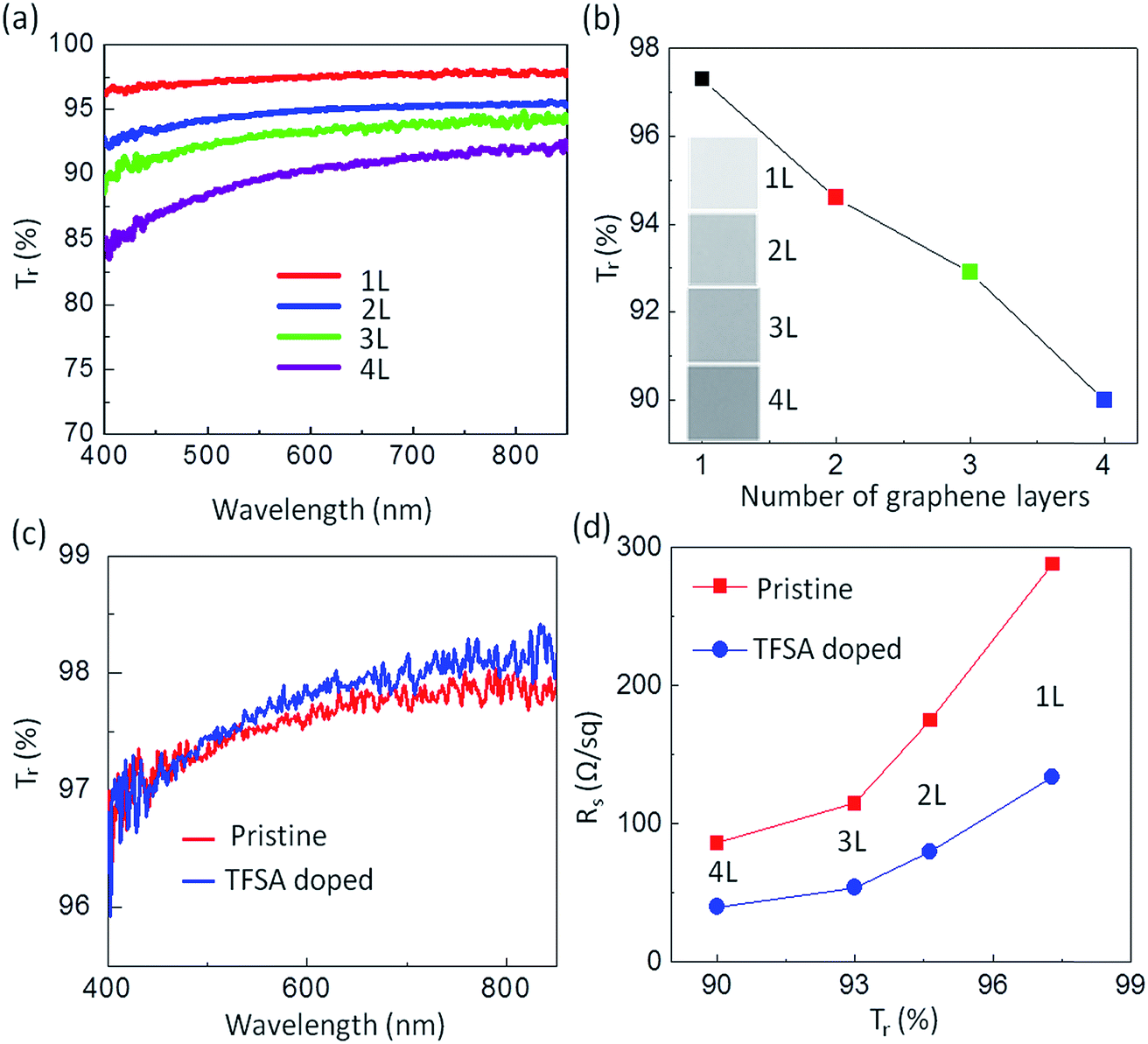 | ||
| Fig. 3 Evaluation of pulsed-grown graphene films as transparent conductor. (a) Transmittance spectra of one- to four-layer stacked graphene films in the visible region of the energy spectrum. (b) Tr (%) as a function of the number of graphene layers extracted from (a) at λ = 550 nm. Inset shows photographs of stacked graphene layers. (c) Comparison of transmittance spectra between one-layer pristine graphene and TFSA-doped graphene. (d) Rsvs. Tr (%) of pristine and TFSA-doped graphene films for one to four stacked layers. | ||
Fig. 4a compares the sheet resistance of our graphene films prepared by pulsed-grown method with some others reported in literature as a function of Tr at λ = 550 nm. An extremely low Rs of 40 Ω sq−1 was observed for TFSA-doped four-layer stacked graphene films at a Tr of 90%. Such a low value of Rs is promising for designing an extremely efficient transparent conductor, and the Tr value is almost comparable with that of ITO.62,63 The Rs of our pristine and TFSA-doped graphene films is very low compared to that of wet transferred graphene61 and HNO3-doped graphene.60 However, these values are a little higher than the theoretical calculated values.64 These higher experimental Rs values could be due to the presence of small metallic contaminants on the graphene surface during the transfer process. For the monolayer case, the Rs of prepared graphene films is also low compared to CHCl3-doped graphene24 and annealed and polished graphene,65 but a little higher than KI-doped graphene.66
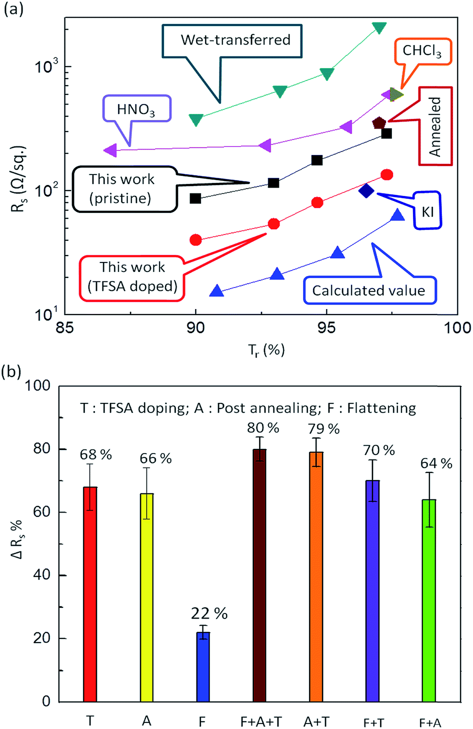 | ||
| Fig. 4 (a) Comparison of Rs of the pulsed-grown graphene films with those reported in the literature as a function of Tr (%) at λ = 550 nm. An extremely low Rs of 40 Ω sq−1 was observed for TFSA-doped four-layer stacked graphene films at a Tr of 90%, which is almost comparable with that of ITO.62,63 The Rs values of pristine (black squares) and TFSA-doped graphene films (red circles) of the present work are very low compared to those of wet transferred graphene (blue-green triangles)61 and HNO3 doped graphene (purple triangles).60 However, these values are slightly higher than the theoretical calculated values.64 For the monolayer case, the Rs of the present graphene films is also low compared to CHCl3-doped graphene (olive-green triangle)24 and annealed graphene (chocolate-brown pentagon),65 but slightly higher than KI-doped graphene (blue diamond).66 (b) Reduction in Rs (ΔRs) of graphene films by TFSA doping (T), post annealing (A), flattening (F) and some combination of these processes. The maximum ΔRs is 68% for TFSA doping compared to post annealing (66%) and flattening (22%). The combination of all three effects (T + A + F) shows maximum ΔRs of 80%, whereas other combinations (A + T), (F + T) and (A + F) show ΔRs of 79, 70 and 64%, respectively. | ||
Besides TFSA doping (T), I carried out post annealing (A) and flattening (F) of graphene films to reduce the Rs, as shown in Fig. 4b. The maximum reduction in the Rs (ΔRs) was observed for T (68%) compared to A (66%) and F (22%). Interestingly, the combination of all three effects (T + A + F) shows a maximum ΔRs of 80%, whereas other combinations (A + T), (F + T) and (A + F) show ΔRs of 79%, 70% and 64%, respectively. The above methods also have been applied to graphene prepared by continuous CH4 flow in literature, including TFSA doping,19,33,67 annealing,35,36 and stacking,7,23,24 as shown in ESI Table S1.† The reduction is Rs value is 30–75%, 7–30% and 50–58% for TFSA doping, annealing and stacking, respectively, which are comparatively less with reference to pulsed-grown graphene. During post annealing, the residual PMMA present on the surface of graphene decomposes at a temperature > 160 °C.49 It is expected that the decomposition products of this molecule form cross links with the graphene surface by forming dangling bonds, and the surface absorbs O2 or water vapor during cooling to room temperature, becoming heavily p-doped, which leads to increased conductance. Flattening of graphene films was carried out using PMMA, in which the PMMA/graphene stack was prepared and heated at elevated temperatures (∼150–160 °C). Heating of PMMA resulted in softening and expanding PMMA, allowing it to relax flat upon the substrate and thereby minimizing any wrinkling of the graphene, in turn restricting mechanical and electrical degradation, as reported by Goniszewski et al.37 However, the effect of flattening was found to be very insignificant compared to TFSA doping and post annealing (Fig. 4b).
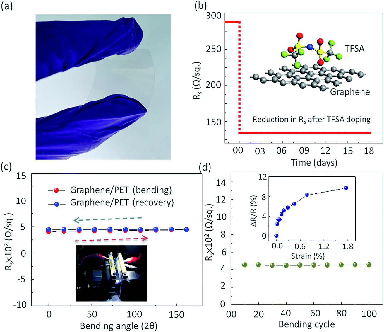
In addition to high optical Tr and low Rs, the graphene film should show excellent mechanical flexibility when used to make flexible and stretchable electrodes.68 In order to investigate the mechanical flexibility of the present graphene films, the pristine as well as the doped monolayer graphene films were transferred onto a 125 μm thick polyethylene terephthalate (PET) substrate coated with a thin PDMS layer (Nan Ya Plastics Corporation, Taiwan (BH216)). Prior to graphene transfer, 30 nm SiO2 was deposited on PET by E-gun evaporation technique to reduce its surface roughness. Fig. 5a shows the photograph of highly transparent graphene film transferred onto flexible PET substrate. To check the environmental stability of TFSA doping, the Rs of TFSA-doped graphene was measured for several days (Fig. 5b). Interestingly, there was no deterioration in Rs observed, even after 18 days, endorsing its superior environmental stability. Fig. 5c presents the Rs of pristine graphene film for bending-recovery cycles. For each cycle, graphene/PET was first bent to an angle of 162° (radius of curvature = 0.35 mm) with an interval of 18° and then fully relaxed in the subsequent interval. The schematic diagram of graphene/PET bending is shown in Fig. S7 (see ESI†). The arrows indicate the direction of bending and recovery. Prior to bending, the Rs of pristine graphene/PET was 419 Ω sq−1, which is higher than the 288 Ω sq−1 observed for graphene/SiO2, and this is probably due to the high RMS surface roughness of PET (4.3 nm) compared to pure SiO2 (1 nm). During bending, there was slight increase in the Rs, then it recovered after releasing the stress. This process was performed through the repeated bending and relaxing steps up to 100 cycles (Fig. 5d). Interestingly, the Rs remained unperturbed up to 100 bending cycles, which demonstrates the high flexibility of the prepared graphene film, similar to those observed by other groups.69,70
 | ||
| Fig. 5 Analysis of electromechanical properties of graphene films. (a) Photograph showing highly transparent graphene film transferred onto flexible PET substrate. (b) Reduction in Rs of graphene film after TFSA doping and its environmental stability test. The Rs remains preserved up to 18 days, revealing superior environmental stability. (c) The Rsvs. bending angle of pristine graphene measured on PET substrate under different bending conditions. The arrows show the direction of bending and recovery. Inset shows a photograph of the mechanical flexibility test setup. (d) The Rsvs. bending cycles for single-layer graphene/PET substrate. The Rs remains unperturbed up to 100 bending cycles. Inset shows the relative change in Rsversus strain due to bending. At a maximum tensile strain of 1.77%, the Rs of the graphene film increased by 10–11% only. | ||
Bending of PET substrate produced surface strain on the graphene/PET film. The tensile strain was determined by the relatively extended length of graphene film upon bending of the underlying supporting PET substrate.71 By assuming the length of the neutral axis of flat PET to be L0, which changes with respect to the subsequent bending angle (θ), the bending radius (r) was calculated using L0 = r × θ. Furthermore, the uniaxial tensile strain was calculated from the following relation,72,73
 | (3) |
Experimental
Modified graphene growth process
Graphene sheets used in the current study were grown by atmospheric pressure chemical vapor deposition (APCVD) on polycrystalline Cu foils, using methane (99.99%) as carbon source. Prior to growth, the Cu foils were cleaned with acetone and isopropyl alcohol (IPA) by sonication, followed by etching in acetic acid for 30 min to remove surface oxides. Then, the Cu foils were mounted in the CVD chamber, and graphene growth process was configured in several steps in the presence of steady flow of hydrogen and argon gas in the proportion of 10–20![[thin space (1/6-em)]](https://www.rsc.org/images/entities/char_2009.gif) :300 sccm. The schematic of the growth process is shown in Fig. S1 (see ESI†). In the first step, the furnace was ramped up to 1050 °C over 40 min. In the second step, pre-annealing was carried out by holding the temperature at 1050 °C for 30 min. By this step, the oxide on the copper foil surface was being removed and the internal stress was released by recrystallization to make the surface of copper foil smoother. Then, methane with flow rate of <1 sccm was fed into the reaction chamber for 50 min (15–25 cycles) in step 3, during which graphene growth occurred. In each cycle, CH4 pulse was given for 30 s and then released for 1 min. This process was carried out by means of a control device, which controlled the import flow rate of the CH4 gas by controlling the opening and closing of the gas valve. That is to say, the CH4 supply during this reaction step was changed continuously (first increased and then decreased in one cycle), which is different from the constant gas supply process in prior literature. Finally, the Cu foils were moved to the cooling zone, which is equipped with a cooling system, in step 4.
:300 sccm. The schematic of the growth process is shown in Fig. S1 (see ESI†). In the first step, the furnace was ramped up to 1050 °C over 40 min. In the second step, pre-annealing was carried out by holding the temperature at 1050 °C for 30 min. By this step, the oxide on the copper foil surface was being removed and the internal stress was released by recrystallization to make the surface of copper foil smoother. Then, methane with flow rate of <1 sccm was fed into the reaction chamber for 50 min (15–25 cycles) in step 3, during which graphene growth occurred. In each cycle, CH4 pulse was given for 30 s and then released for 1 min. This process was carried out by means of a control device, which controlled the import flow rate of the CH4 gas by controlling the opening and closing of the gas valve. That is to say, the CH4 supply during this reaction step was changed continuously (first increased and then decreased in one cycle), which is different from the constant gas supply process in prior literature. Finally, the Cu foils were moved to the cooling zone, which is equipped with a cooling system, in step 4.
Graphene transfer process using PMMA
Graphene layers on Cu foils were coated with 300 nm thick PMMA, followed by etching in a 16.5% aqueous hydrochloric acid solution. The PMMA film, along with the attached graphene, was detached from the metal substrate after a whole night. The PMMA/graphene film was then rinsed with DI water, transferred to a silicon or target substrate, and rinsed with warm acetone to remove the PMMA. Photographs of the graphene transfer process are shown in Fig. S4 (see ESI†).Experimental methods to reduce sheet resistance
TFSA-doped graphene was prepared by spinning a few droplets of TFSA over graphene film at 3000 rpm for 30 s. Post annealing was carried out in two steps, first at 250 °C in air and then at 250 °C in the presence of mixed H2 (200 sccm) and Ar (400 sccm) atmosphere for 2 h, similar to Lin et al.49 Flattening of graphene film was performed by spin coating of PMMA at 3000 rpm for 30 s, followed by heating at elevated temperatures (∼150–160 °C) and, finally, removing PMMA using warm acetone. Stacked graphene films were prepared by sequential transfer of one graphene layer over another, up to four layers. No adhesive was used at the interfaces, and the interlayer bonding is only due to van der Waals force.Band structure calculation of TFSA-doped graphene
Band structure calculation was performed by placing the TFSA molecule on the top of single-layer graphene. The pseudopotential density functional SIESTA package was used for band structure calculations,75,76 with the local density approximation (LDA) representing the exchange correlation potential77,78 and with an energy mesh cutoff of 150 Ry. Optimization of initial experimental structures was performed using analytical energy gradient with respect to atomic coordinates and unit cell parameters. The structures were relaxed until the force on each atom was less than 0.01 eV Å−1. The Brillouin zone was sampled with a grid of 5 × 5 × 1 k-points within the Monkhorst–Pack scheme.79 Band structures were calculated along the high symmetry points using the path Г–M–K–Г.Conclusions
In summary, high-quality graphene was prepared by supplying methane pulses instead of the conventional continuous methane flow used in CVD. The lowest sheet resistance of a few hundred Ω sq−1, the on/off ratio of ∼13 for the graphene-based FET, and the high I2D/IG ratio of >1.5 demonstrate the quantitative signatures of graphene quality. Several processes, including TFSA doping, post annealing, flattening and stacking of graphene films, were carried out in order to reduce the sheet resistance, making them suitable for application as transparent conducting electrode. An extremely low sheet resistance of 40 Ω sq−1 for TFSA-doped four-layer stacked graphene films at a transmittance of 90% was reported, which is almost comparable with that of ITO. TFSA doping was found to be very effective for increasing the conductivity of graphene film. Interestingly, the combination of TFSA doping, post annealing and flattening of graphene films was found to reduce the sheet resistance by 80%, which is the highest value reported so far. Besides, the superior mechanical flexibility of this highly conducting and transparent film was also demonstrated, making it suitable as a transparent conducting electrode. This work provides a new pathway to obtain a suitable transparent conducting electrode for applications in various optoelectronic devices such as solar cells, touch screens, and transparent displays in the future.Conflicts of interest
There are no conflicts to declare.Acknowledgements
The author would like to acknowledge the financial support from the Department of Science and Technology, India, with sanction order No. SERB/F/5379/2017-2018 under Ramanujan Fellowship. The author also acknowledges Chao-Hui Yeh of National Tsing Hua University, Taiwan, for graphene transfer as well as useful discussion.Notes and references
- A. Kumar and C. Zhou, ACS Nano, 2010, 4, 11–14 CrossRef CAS.
- D. S. Hecht, L. Hu and G. Irvin, Adv. Mater., 2011, 23, 1482–1513 CrossRef CAS PubMed.
- J. Du, S. Pei, L. Ma and H. M. Cheng, Adv. Mater., 2014, 26, 1958–1991 CrossRef CAS PubMed.
- J. Ning, L. Hao, M. Jin, X. Qiu, Y. Shen, J. Liang, X. Zhang, B. Wang, X. Li and L. Zhi, Adv. Mater., 2017, 29, 1605028 CrossRef PubMed.
- H. Kim, J. S. Horwitz, G. Kushto, A. Piqué, Z. H. Kafafi, C. M. Gilmore and D. B. J. Chrisey, J. Appl. Phys., 2000, 88, 6021–6025 CrossRef CAS.
- L. G. De Arco, Y. Zhang, C. W. Schlenker, K. Ryu, M. E. Thompson and C. Zhou, ACS Nano, 2010, 4, 2865–2873 CrossRef PubMed.
- A. Kasry, M. A. Kuroda, G. J. Martyna, G. S. Tulevski and A. A. Bol, ACS Nano, 2010, 4, 3839–3844 CrossRef CAS PubMed.
- R. R. Nair, P. Blake, A. N. Grigorenko, K. S. Novoselov, T. J. Booth, T. Stauber, N. M. R. Peres and A. K. Geim, Science, 2008, 320, 1308 CrossRef CAS PubMed.
- X. Huang, T. Leng, M. Zhu, X. Zhang, J. Chen, K. Chang, M. Aqeeli, A. K. Geim, K. S. Novoselov and Z. Hu, Sci. Rep., 2015, 5, 18298 CrossRef CAS PubMed.
- S. Chen, L. Brown, M. Levendorf, W. Cai, S. Y. Ju, J. Edgeworth, X. Li, C. W. Magnuson, A. Velamakanni, R. D. Piner, J. Kang, J. Park and R. S. Ruoff, ACS Nano, 2011, 5, 1321–1327 CrossRef CAS PubMed.
- P. K. Nayak, C. J. Hsu, S. C. Wang, J. C. Sung and J. L. Huang, Thin Solid Films, 2013, 529, 312–316 CrossRef CAS.
- K. S. Kim, Y. Zhao, H. Jang, S. Y. Lee, J. M. Kim, K. S. Kim, J. H. Ahn, P. Kim, J. Y. Choi and B. H. Hong, Nature, 2009, 457, 706–710 CrossRef CAS PubMed.
- J. B. Wu, M. Agrawal, H. A. Becerril, Z. N. Bao, Z. F. Liu, Y. S. Chen and P. Peumans, ACS Nano, 2010, 4, 43–48 CrossRef CAS PubMed.
- T. Kobayashi, M. Bando, N. Kimura, K. Shimizu, K. Kadono, N. Umezu, K. Miyahara, S. Hayazaki, S. Nagai, Y. Mizuguchi, Y. Murakami and D. Hobara, Appl. Phys. Lett., 2013, 102, 023112 CrossRef.
- A. Ford, Graphene for Transparent Conductive Film Applications, LAP LAMBERT Academic Publishing, 2016 Search PubMed.
- P. P. Edwards, A. Porch, M. O. Jones, D. V. Morgan and R. M. Perks, Dalton Trans., 2004, 2995–3002 RSC.
- K. K. Kim, A. Reina, Y. Shi, H. Park, L. J. Li, Y. H. Lee and J. Kong, J. Nanotechnol., 2010, 21, 285205 CrossRef PubMed.
- S. Bae, H. Kim, Y. Lee, X. Xu, J. S. Park, Y. Zheng, J. Balakrishnan, T. Lei, H. R. Kim, Y. I. Song, Y. J. Kim, K. S. Kim, B. Özyilmaz, J. H. Ahn, B. H. Hong and S. Iijima, Nat. Nanotechnol., 2010, 5, 574–578 CrossRef CAS PubMed.
- X. Miao, S. Tongay, M. K. Petterson, K. Berke, A. G. Rinzler, B. R. Appleton and A. F. Hebard, Nano Lett., 2012, 12, 2745–2750 CrossRef CAS PubMed.
- J. O. Hwang, J. S. Park, D. S. Choi, J. Y. Kim, S. H. Lee, K. E. Lee, Y. H. Kim, M. H. Song, S. Yoo and S. O. Kim, ACS Nano, 2012, 6, 159–167 CrossRef CAS PubMed.
- L. D. Arsié, S. Esconjauregui, R. S. Weatherup, X. Wu, W. E. Arter, H. Sugime, C. Cepek and J. Robertson, RSC Adv., 2016, 6, 113185–113192 RSC.
- M. Kim, K. J. Kim, S. J. Lee, H. M. Kim, S. Y. Cho, M. S. Kim, S. H. Kim and K. B. Kim, ACS Appl. Mater. Interfaces, 2017, 9, 701–709 CrossRef CAS PubMed.
- Y. Xu, H. Yu, C. Wang, J. Cao, Y. Chen, Z. Ma, Y. You, J. Wan, X. Fang and X. Chen, Nanoscale Res. Lett., 2017, 12, 254 CrossRef PubMed.
- J. S. Choi, H. Choi, K. C. Kim, H. Y. Jeong, Y. J. Yu, J. T. Kim, J. S. Kim, J. W. Shin, H. Cho and C. G. Choi, Sci. Rep., 2016, 6, 24525 CrossRef CAS PubMed.
- B. Chandra, A. Afzali, N. Khare, M. M. El-Ashry and G. S. Tulevski, Chem. Mater., 2010, 22, 5179–5183 CrossRef CAS.
- C. Yan, K. S. Kim, S. K. Lee, S. H. Bae, B. H. Hong, J. H. Kim, J. H. Kim, H. J. Lee and J. H. Ahn, ACS Nano, 2012, 6, 2096–2103 CrossRef CAS PubMed.
- F. Schedin, A. K. Geim, S. V. Morozov, E. W. Hill, B. Blake, M. I. Katsnelson and K. S. Novoselov, Nat. Mater., 2007, 6, 652–655 CrossRef CAS PubMed.
- K. Rakhimov, A. Chaves and P. Lambin, Appl. Sci., 2016, 6, 256–266 CrossRef.
- A. Capasso, T. Dikonimos, F. Sarto, A. Tamburrano, G. De Bellis, M. S. Sarto, G. Faggio, A. Malara, G. Messina and N. Lisi, Beilstein J. Nanotechnol., 2015, 6, 2028–2038 CrossRef CAS PubMed.
- G. H. Kim and S. Jeong, Sci. Rep., 2015, 5, 11227 CrossRef PubMed.
- Z. Han, A. Kimouche, D. Kalita, A. Allain, H. A. Tash, A. R. Plantey, L. Marty, S. Pairis, V. Reita, N. Bendiab, J. Coraux and V. Bouchiat, Adv. Funct. Mater., 2014, 24, 964–970 CrossRef CAS.
- Y. C. Lai, B. S. Wu, S. C. Yu, P. Yu and G. C. Chi, IEEE Conf., 2013, 2436–2438 CAS.
- S. Tongay, K. Berke, M. Lemaitre, Z. Nasrollahi, D. B. Tanner, A. F. Hebard and B. R. Appleton, Nanotechnology, 2011, 22(1–6), 425701 CrossRef CAS PubMed.
- F. Bausi, A. Schlierf, E. Treossi, M. G. Schwab, V. Palermo and F. Cacialli, Org. Electron., 2015, 18, 53–60 CrossRef CAS.
- O. V. Tolochko, T. V. Larionova, T. S. Koltsova, M. V. Kozlova, E. V. Bobrynina, O. A. Martynova and V. E. Gasumyants, J. Phys.: Conf. Ser., 2017, 816, 012012 CrossRef.
- W. Choi, Y. S. Seo, J. Y. Park, K. B. Kim, J. Jung, N. Lee and Y. Seo, IEEE Trans. Nanotechnol., 2015, 14, 70–74 Search PubMed.
- S. Goniszewski, J. Gallop, M. Adabi, K. Gajewski, E. Shaforost, N. Klein, A. Sierakowski, J. Chen, Y. Chen, T. Gotszalk and L. Hao, IET Circuits, Devices Syst., 2015, 9, 420–427 CrossRef.
- X. Li, W. Cai, J. An, S. Kim, J. Nah, D. Yang, R. Piner, A. Velamakanni, I. Jung, E. Tutuc, S. K. Banerjee, L. Colombo and R. S. Ruoff, Science, 2009, 324, 1312 CrossRef CAS PubMed.
- Y. C. Lin, C. H. Jin, J. C. Lee, S. F. Jen, K. Suenaga and P. W. Chiu, ACS Nano, 2011, 5, 2362–2368 CrossRef CAS PubMed.
- X. Li, L. Colombo and R. S. Ruoff, Adv. Mater., 2016, 28, 6247–6252 CrossRef CAS PubMed.
- H. S. Song, S. L. Li, H. Miyazaki, S. Sato, K. Hayashi, A. Yamada, N. Yokoyama and K. Tsukagoshi, Sci. Rep., 2012, 2, 337 CrossRef CAS PubMed.
- V. Kochat, C. S. Tiwary, T. Biswas, G. Ramalingam, K. Hsieh, K. Chattopadhyay, S. Raghavan, M. Jain and A. Ghosh, Nano Lett., 2016, 16, 562–567 CrossRef CAS PubMed.
- G. H. Han, F. Günes, J. J. Bae, E. S. Kim, S. J. Chae, H. J. Shin, J. Y. Choi, D. Pribat and Y. H. Lee, Nano Lett., 2011, 11, 4144–4148 CrossRef CAS PubMed.
- Y. Ogawa, K. Komatsu, K. Kawahara, M. Tsuji, K. Tsukagoshi and H. Ago, Nanoscale, 2014, 6, 7288–7294 RSC.
- H. Zhou, W. J. Yu, L. Liu, R. Cheng, Y. Chen, X. Huang, Y. Liu, Y. Wang, Y. Huang and X. Duan, Nat. Commun., 2013, 4, 2096 CrossRef PubMed.
- L. P. Biŕo and P. Lambin, New J. Phys., 2013, 15, 035024 CrossRef.
- X. Chen, L. Zhang and S. Chen, Synth. Met., 2015, 210, 95–108 CrossRef CAS.
- I. V. Antonova, Phys.-Usp., 2013, 183, 1115–1122 Search PubMed.
- Y. C. Lin, C. C. Lu, C. H. Yeh, C. Jin, K. Suenaga and P. W. Chiu, Nano Lett., 2012, 12, 414–419 CrossRef CAS PubMed.
- T. J. Ha, J. Lee, D. Akinwande and A. Dodabalapur, IEEE Electron Device Lett., 2013, 34, 559–561 CAS.
- J. W. Suk, W. H. Lee, J. Lee, H. Chou, R. D. Piner, Y. Hao, D. Akinwande and R. S. Ruoff, Nano Lett., 2013, 13, 1462–1467 CrossRef CAS PubMed.
- S. M. Kim, Y. W. Jo, K. K. Kim, D. L. Duong, H. J. Shin, J. H. Han, J. Y. Choi, J. Kong and Y. H. Lee, ACS Nano, 2010, 4, 6998–7004 CrossRef CAS PubMed.
- D. Kim, D. Lee, Y. Lee and D. Y. Jeon, Adv. Funct. Mater., 2013, 23, 5049–5055 CrossRef CAS.
- M. A. B. H. Susan, A. Noda, S. Mitsushima and M. Watanabe, Chem. Commun., 2003, 938–939 RSC.
- M. Pykal, P. Jurečka, F. Karlický and M. Otyepka, Phys. Chem. Chem. Phys., 2016, 18, 6351–6372 RSC.
- B. J. Schultz, R. V. Dennis, V. Lee and S. Banerjee, Nanoscale, 2014, 6, 3444–3466 RSC.
- A. C. Ferrari, J. C. Meyer, V. Scardaci, C. Casiraghi, M. Lazzeri, F. Mauri, S. Piscanec, D. Jiang, K. S. Novoselov, S. Roth and A. K. Geim, Phys. Rev. Lett., 2006, 97, 187401 CrossRef CAS PubMed.
- R. Parret, M. Paillet, J. R. Huntzinger, D. Nakabayashi, T. Michel, A. Tiberj, J. L. Sauvajol and A. A. Zahab, ACS Nano, 2013, 7, 165–173 CrossRef CAS PubMed.
- P. Blake, P. D. Brimicombe, R. R. Nair, T. J. Booth, D. Jiang, F. Schedin, L. A. Ponomarenko, S. V. Morozov, H. F. Gleeson, E. W. Hill, A. K. Geim and K. S. Novoselov, Nano Lett., 2008, 8, 1704–1708 CrossRef PubMed.
- G. Gao, W. Gao, E. Cannuccia, J. T. Tijerina, L. Balicas, A. Mathkar, T. N. Narayanan, Z. Liu, B. K. Gupta, J. Peng, Y. Yin, A. Rubio and P. M. Ajayan, Nano Lett., 2012, 12, 3518–3525 CrossRef CAS PubMed.
- X. Li, Y. Zhu, W. Cai, M. Borysiak, B. Han, D. Chen, R. D. Piner, L. Colombo and R. S. Ruoff, Nano Lett., 2009, 9, 4359–4363 CrossRef CAS PubMed.
- H. Kim, J. S. Horwitz, G. P. Kushto, Z. H. Kafafi and D. B. Chrisey, Appl. Phys. Lett., 2001, 79, 284 CrossRef CAS.
- F. L. Wong, M. K. Fung, S. W. Tong, C. S. Lee and S. T. Lee, Thin Solid Films, 2004, 466, 225–230 CrossRef CAS.
- F. Bonaccorso, Z. Sun, T. Hasan and A. C. Ferrari, Nat. Photonics, 2010, 4, 611–622 CrossRef CAS.
- J. K. Lee, C. S. Park and H. Kim, RSC Adv., 2014, 4, 62453–62456 RSC.
- M. Kim, A. Shah, C. Li, P. Mustonen, J. Susoma, F. Manoocheri, J. Riikonen and H. Lipsanen, 2D Mater., 2017, 4, 035004 CrossRef.
- Y. C. Lai, B. S. Wu, S. C. Yu, P. Yu and G. C. Chi, IEEE Conf., 2013, 2436–2438 CAS.
- C. Lee, X. Wei, J. W. Kysar and J. Hone, Science, 2008, 321, 385–388 CrossRef CAS PubMed.
- L. G. De Arco, Y. Zhang, C. W. Schlenker, K. Ryu, M. E. Thompson and C. Zhou, ACS Nano, 2010, 4, 2865–2873 CrossRef PubMed.
- Z. Yin, S. Sun, T. Salim, S. Wu, X. Huang, Q. He, Y. M. Lam and H. Zhang, ACS Nano, 2010, 4, 5263–5268 CrossRef CAS PubMed.
- T. Yu, Z. Ni, C. Du, Y. You, Y. Wang and Z. Shen, J. Phys. Chem. C, 2008, 112, 12602–12605 CrossRef CAS.
- S. Takamatsu, T. Takahata, M. Muraki, E. Iwase, K. Matsumoto and I. Shimoyama, J. Micromech. Microeng., 2010, 20(1–6), 075017 CrossRef.
- N. Lu, C. Lu, S. Yang and J. Rogers, Adv. Funct. Mater., 2012, 22, 4044–4050 CrossRef CAS.
- S. Lee, K. Lee, C. H. Liu and Z. Zhong, Nanoscale, 2011, 4, 639–644 RSC.
- Quantum Wise A/S, Atomistix Tool Kit, 2010, ch. 10.8.2 Search PubMed.
- M. Brandbyge, J. Mozos, P. Ordejon, J. Taylor and K. Stokbro, Phys. Rev. B, 2002, 65, 165401 CrossRef.
- D. M. Ceperley and B. J. Alder, Phys. Rev. Lett., 1980, 45, 566 CrossRef CAS.
- J. P. Perdew and A. Zunger, Phys. Rev. B, 1981, 23, 5048 CrossRef CAS.
- H. J. Monkhorst and J. D. Pack, Phys. Rev. B, 1976, 13, 5188 CrossRef.
Footnote |
| † Electronic supplementary information (ESI) available: Experimental details for the modified graphene growth, growth mechanism, experimental processes to reduce sheet resistance, graphene transfer process, sheet resistance measurement, flexibility test and reduction of sheet resistance in continuous flow graphene are given in Fig. S1–S7† and Table S1,† respectively. This material is available free of charge from the Royal Society of Chemistry (RSC) online library or from the author. See DOI: 10.1039/c8na00181b |
| This journal is © The Royal Society of Chemistry 2019 |