
 Open Access Article
 This Open Access Article is licensed under a Creative Commons Attribution-Non Commercial 3.0 Unported Licence
Assessment of three electrolyte–molecule electrostatic interaction models for 2D material based BioFETs
A.
Toral-Lopez†
 *a,
E. G.
Marin
ab,
J. M.
Gonzalez-Medina†
a,
F. J.
Romero†
a,
F. G.
Ruiz†
a,
D. P.
Morales
a,
N.
Rodriguez†
a and
A.
Godoy†
*a
*a,
E. G.
Marin
ab,
J. M.
Gonzalez-Medina†
a,
F. J.
Romero†
a,
F. G.
Ruiz†
a,
D. P.
Morales
a,
N.
Rodriguez†
a and
A.
Godoy†
*a
aDpto. Electrónica, Fac. Ciencias, Universidad de Granada, 18071, Spain. E-mail: agodoy@ugr.es; atoral@ugr.es
bDipartimento di Ingegneria dell'Informazione, Università di Pisa, 56122 Pisa, Italy
First published on 30th November 2018
Abstract
BioFETs based on two-dimensional materials (2DMs) offer a unique opportunity to enhance, at a low cost, the sensitivity of current biosensors enabling the design of compact devices compatible with standard CMOS technology. The unique combination of large exposed surface areas and minimal thicknesses of 2DMs is an outstanding feature for these devices, and the assessment of their behaviour requires combined experimental and theoretical efforts. In this work we present a 2D-material based BioFET simulator including complex electrolyte reactions and analysing different models for the electrolyte–molecule interaction. These models describe how the molecular charge is screened by the electrolyte ions when their distributions are modified. The electrolyte simulation is validated against experimental results as well as against the analytical predictions of the Debye–Hückel approximation. The role of the electrolyte charge screening as well as the impact of the interaction model on the device responsivity are analysed in detail. The results are discussed in order to conclude about the consequences of employing different interaction approximations for the simulation of BioFETs and more generally on the correct modelling of biomolecule-device interaction in BioFETs.
1 Introduction
The rapid detection and continuous monitoring of biological and chemical compounds are of great interest for medical and security purposes, including e.g. point-of-care solutions, drug detection, genomics, homeland security, etc.1 State-of-the-art systems are, primarily, label-based methods i.e. the sample is processed to allow the detection of target molecules via measurable parameters, like fluorescence or colorimetry. The use of labelling elements in the transduction process analysis presents some disadvantages: it entails high operational costs and lack of portability, and is limited for real-time applications.2 Label-free methods, in contrast, are of high interest in rapid detection and continuous monitoring applications. Field-effect transistor based biosensors (BioFETs) constitute an interesting solution, compatible with standard commercial electronic technologies, reducing the cost and power consumption per device and allowing the integration of the measurement and signal processing stages in the same system.3Although the origin of BioFETs dates back to the 70's and 80's,4–7 it is in the last decade when they have come into the spotlight thanks to the auspicious progress made with new structures and materials. In particular, nanowire-based BioFETs have been demonstrated to notably boost the sensitivity of previous devices.1,8 However, their integration with planar technology is challenging and the shift to the industrial arena is predicted to be limited. This gap is expected to be filled by graphene9 and the two-dimensional (2D) material family (including transition metal dichalcogenides,10 group IV,11,12 group V,13,14etc.), which promises high sensitivity, integration with standard technology and easier surface functionalization.3,15–17 Indeed, several 2D material-based BioFETs have already been successfully fabricated2,3,16–19 and their operating principles are subject of intense research.20–26 This growing interest in the design of new and highly sensitive biosensors based on 2D materials is driven by a myriad of practical applications with an expected huge impact from a technological and economical point of view.
2D BioFETs can be classified into two categories according to the device-target interface:27 electrolyte–insulator–semiconductor (EIS) and electrolyte–semiconductor (ES). In the EIS BioFETs, an insulator layer, placed between the electrolyte and the semiconductor, is functionalized (usually via silanization). The objective of this process is to attach receptor agents (e.g. antibody-(TNF-alpha), PSA-mAb), able to capture the target molecules.2,3,17 This layer prevents possible reactions between the ions contained in the solution and the semiconductor surface, but it reduces the electrical coupling between the device and the molecules.27 In addition, most of the materials used as gate insulators have a hydrophilic nature that hinders the functionalization and reduces the efficiency of the bindings.16 In ES BioFETs, the insulator layer is removed leaving the semiconductor directly in contact with the electrolyte. In these devices, the semiconductor surface must be functionalized, although some biosensors without the functionalization layer have also been tested.16,28 These experiments have shown that the bare surface can be enough to trap the molecules, but not selectively, resulting in a weak modulation of the device response. Amongst 2D materials, MoS2, reduced graphene oxide (r-GO) and graphene show a hydrophobic behaviour and are good candidates to be employed in ES BioFETs.16,17,29,30 Indeed, the hydrophobic nature of these materials improves the quality of the molecular bindings16 and the absence of the insulator enhances the coupling between the target molecules and the semiconductor channel. ES BioFETs can be classified according to the measurement process, i.e. if the device surface is dried after the exposure to the analyte and before its electrical characterization (so-called dry environments), or if it is kept in contact with the sample during the measurement process (so-called wet environments). The former is a simpler alternative and has been demonstrated on a MoS2 channel driven by a back gate.16 Dry devices show some additional advantages: a simplified processing, the avoidance of molecule attaching/detaching events as a source of noise, and the availability of rapid measurement methods.31 However, they cannot be used for in vivo measurements where it is not easy to control, or to dry, the environment and have, therefore, limited application. In contrast, in wet devices the electrolyte is preserved.
In this work, we will focus on the structures where the electrolyte is present, and specifically on the modelling of the interaction between the electrolyte ions and the target molecules attached to the sensing interface. The BioFET simulation has been so far carried out using either commercial TCAD simulators,20–23 which are not purpose-designed to include the electrolyte effects, or ad hoc software.24–26 In particular, TCAD simulators make coarse approximations to model the effect of the electrolyte and biomolecules. First, the electrolyte is commonly modelled as a semiconductor with modified characteristics trying to fit its actual behaviour.22,23 Although the approach is useful for simple electrolytes, there are important limitations when multiple types of ions are present in the solution.22 Second, the biomolecules are usually modelled as a set of charged blocks immersed in the electrolyte close to the device surface (typically one block per attached molecule). This approach results in a set of blocks equally distributed along the device surface.20,21 Uncharged blocks are associated with unattached molecules resulting in unrealistic potential distributions in the electrolyte region, blocking the distribution of ions. The modelling of the semiconductor is, in contrast, performed in detail as it corresponds to the specific purpose of those software packages.
In ad hoc simulators, differently, specific equations governing the electrolyte are used. Therefore, a more realistic description of the device can be carried out incorporating in the model: (i) non-linear effects (e.g. surface ion adsorption making use of the site-binding model5,32) and (ii) the specific characteristics of the molecules such as their orientation with respect to the device surface or their dipole moment.24,26 In addition, complex electrolytes with multiple ion species can be simulated without coarse approximations. However, these numerical tools are oriented to specific structures, mainly nanowires25,26 and planar devices with bulk semiconductors,24 paying little attention to 2D materials, and the options to reconfigure the structure are very limited in comparison with TCADs. Despite the detailed study of the electrolyte, the modelling of the interaction with molecules attached to the device surface is frequently missed. Most of the studies describe the modelling of the electrolyte ionic charges but, they do not clarify how the molecular charges are implemented. This interaction between the target molecules and the electrolyte via charge screening remains elusive. It is a fundamental point to understand and reproduce the operation of BioFETs,1 and therefore deserves attention.
In this context, a comprehensive understanding of the working principles of 2D-material based BioFETs and the development of accurate models and simulators become mandatory to accelerate their development. Taking into consideration these principles and the aforementioned technical limitations of the present numerical models, we have developed a simulator which accurately integrates the modelling of both, the 2D semiconductor material and the biological region, which includes the electrolyte and the molecules. It is designed for planar structures which can be easily modified considering different materials for the semiconductor channel and for the layers above and below it. Multiple ion species and their concentration in the solution can be simultaneously included to define the electrolyte composition and the molecule–electrolyte interaction is implemented in distinct manners.
The rest of the paper is organised as follows. First, Section 2 describes the main characteristics of the simulator. The models used for each component of the device are introduced, including those of the electrolyte–biomolecule interaction that will be compared later. In Section 3, the simulation conditions and results are presented. First, a validation of the electrostatic model of the electrolyte is performed, and then the interaction models will be used to compare the impact on the device response. Finally, Section 4 draws the main conclusions.
2 Methods
The modelled device is schematically depicted in Fig. 1. The semiconductor is sandwiched between two insulator layers, a thicker one that acts as a substrate and a thinner one that separates the semiconductor and the electrolyte. There is a certain region of the top oxide surface covered by the receptor layer. The length of this covered region defines the channel length, LCh. The characteristics of the molecules are depicted on the right side of the figure. Each of them is split into two regions: a charged and a neutral one that includes the binding with the receptors placed over the device surface. The reference electrode is simulated as a contact on the top of the electrolyte. This structure is assumed to be invariant along its width.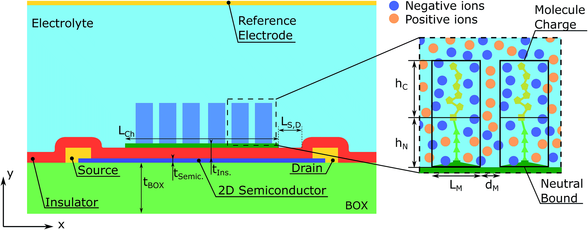 | ||
| Fig. 1 Structure of the 2D-material based EIS BioFETs. The semiconductor channel is sandwiched between two insulator layers, a thicker one that acts as a substrate and another thinner that separates the semiconductor and the electrolyte. A region of the top oxide surface, which is named the receptor layer, is functionalized to capture the target molecules. The characteristics of the latter from the simulation point of view are depicted on the right side of the figure. Each molecule is split into two regions: a charged one and neutral that includes the binding with the receptors. The reference electrode is represented as a contact on the top of the structure. | ||
Two main regions can be distinguished in the structure: the semiconductor region and the biological region, and the latter includes the electrolyte and the biomolecules. The potential distribution, V(x, y), in the whole structure is evaluated by means of the Poisson equation:
| ∇(ε∇V) = −(ρsemic + ρbio) | (1) |
The charge in the semiconductor is evaluated using the Schrödinger equation for thin channels or a 2D Density of States (DoS) under the EMA (Effective Mass Approximation) for 2D materials. In particular, when the Schrödinger equation is considered, it is solved under equilibrium conditions. Next, out of equilibrium, the calculated energy levels are rigidly shifted with the channel potential to determine the charge distribution from the corresponding wavefunctions. This approach, although approximate, is computationally very efficient as compared to the full-blown self-consistent solution. The charge density profile from the source to the drain is obtained from the 1D continuity equation:
 | (2) |
| ρsemic(x,y) = φL(y)·nL(x) | (3) |
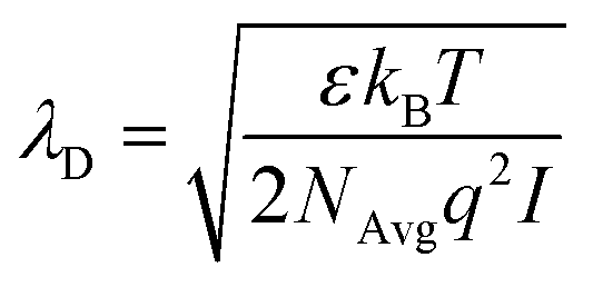
The electrolyte charge comprises the ion and the molecule charge densities. The ion charge density is given by  where NAvg is the Avogadro constant and ci is the i-th ion concentration calculated using a modified Boltzmann equation:22
 | (4) |
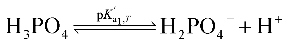
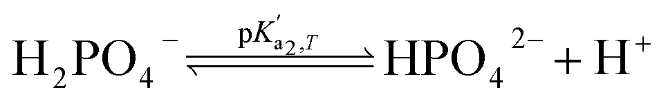
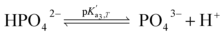
Eqn (4) is used to model regular ions concentrations in the electrolyte. However, it is very common that the electrolyte contains a Phosphate-Buffer Saline (PBS) solution, to stabilize the pH, that must be described differently. The PBS comprises simple salts, the ions of which are modelled by using eqn (4), and compounds that perform the main part of this pH regulation. The concentration of the ions associated with these compounds has an additional component that is defined by a set of chemical reactions. These reactions take place in the solution to modify the local pH concentration (pH = −log10([H+])).33 The PBS considered in this case is based on NaH3PO4, so the reactions involved are the following:
where
 is the temperature-dependent reaction constant, defined as
 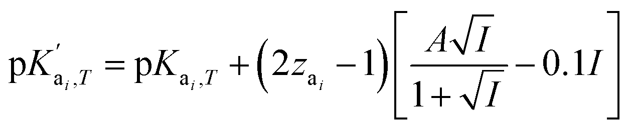 , where A is a temperature-dependent constant, zai the charge of the conjugate acid species, I the ionic strength
 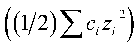 and pKai,T a temperature-dependent coefficient, defined as pKai,T = pKai + dpKai/dT (T – 298.15 K), where T is the temperature in Kelvin and pKa is the reaction constant at T = 298.15 K. The value of the ionic strength I and the pH are calculated locally and used to calculate the PBS ion concentration as:
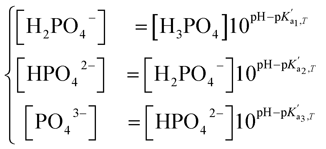 | (5) |
Unlike the ions, the charge and position of the trapped biomolecules are assumed to be fixed. For the sake of simplicity we assume a uniform distribution of molecules in the channel, although an arbitrary distribution could be easily implemented. As depicted in Fig. 1, each molecule is translated into a box of size LM × hM over the channel characterized by a constant charge density ρM, where LM and hM are the length and height of the molecule box, respectively. The number of boxes is defined as NM and the distance between boxes, dM, is modified to distribute them uniformly along the channel. So that, the total number of molecules in the channel can be written as: NM = LCh/(LM + dM). The total charge density in the electrolyte due to the biomolecules can be written as:
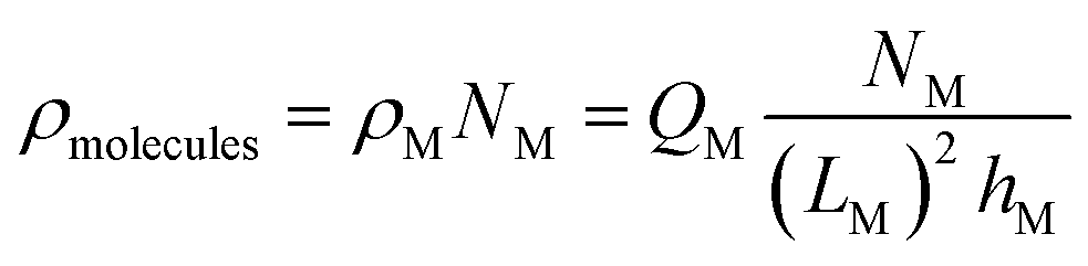 | (6) |
As aforementioned (see Fig. 1), each biomolecule is modelled in two sections, a neutral part, which is the one adhered to the device interface, and a charged region which interacts with the ions in the electrolyte. Based on the different approaches of ref. 34–36, we have considered three descriptions of how these regions constrain the ion distribution so as to assess the differences between them (see Fig. 2):
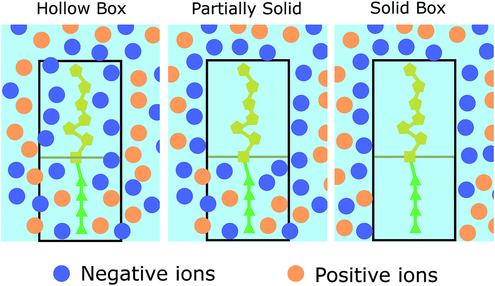 | ||
| Fig. 2 Schematic depiction of the three molecule models. Orange (positive) and blue (negative) circles represent the ions of the electrolyte. Dark yellow pentagons represent the charged part of the molecule and green triangles the neutral section. The molecule as a whole is represented by a black box. | ||
1. Model 1: “Hollow boxes”. Ions are allowed to penetrate in the molecular regions.
2. Model 2: “Partially solid boxes”. Ions are allowed to enter the neutral region of the molecule but not the charged region.
3. Model 3: “Solid boxes”. The molecular regions behave as solid boxes, preventing any ion access.
The differences between these models and their impact on the modelling of a 2D BioFET will be discussed in detail in the next section.
3 Validation and results
The developed simulator has been subjected to a two-step validation process. First a comparison of the numerical model of the isolated electrolyte and the Debye–Hückel analytical approximation has been realized, showing very good agreement. Second, a semiconductor device has been included and its output characteristic is compared with experimental results of a MoS2 BioFET obtained from ref. 3. Later, the role of the molecules, and specifically of the molecule–electrolyte interaction models, is introduced for both systems, the isolated electrolyte and the BioFET device, assessing the differences in the charge screening in the former and the impact on the BioFET responsivity in the latter.3.1 Complex electrolyte simulation
The first validation of the complex electrolyte simulation is performed by evaluating the Debye length of the solution as a function of the ion concentration. The simulated structure is a planar capacitor whose insulator is an electrolyte, as depicted in the inset of Fig. 3b, with permittivity ε = 80ε0 in correspondence of an aqueous base. The electrolyte is a PBS solution, with pH = 7.4, the composition of which is shown in Table 1. Between the electrolyte and one of the plates there is a thin oxide layer (1 nm thick), which represents the insulator over the semiconductor layer. The contact below the oxide layer represents the channel, although in these simulations the potential of this contact is assumed to be fixed, and the other one (in contact with the electrolyte) acts as a reference electrode, set to 0 V. A range of small biases is used for the bottom oxide electrode and the obtained potential profile is compared with an exponential function defined by the Debye–Hückel approximation:| ϕ(x) = ϕ0e−x/λD | (7) |
 | (8) |
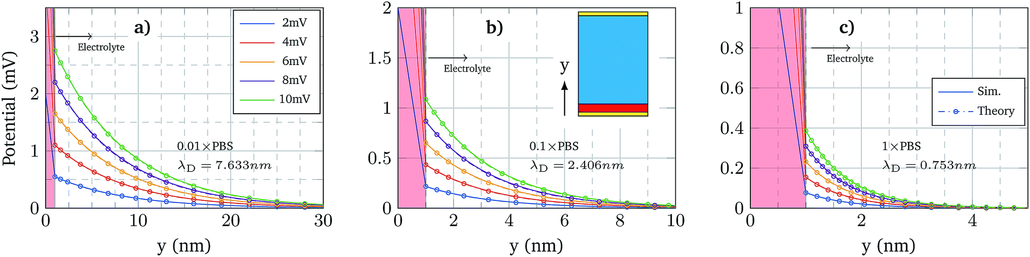 | ||
| Fig. 3 The inset shows the simulated structure: a 1 nm thick insulator (red) in contact with an electrolyte (cyan) between two contacts (gold). The top contact is the reference one and it is fixed to 0 V. The three plots show the potential profile near the oxide surface (solid lines) using different oxide contact potentials and the Debye–Hückel approximation for each case (circles). The oxide region, where the Debye–Hückel approximation does not apply, is coloured in red background. From left to right, the PBS concentration used is 0.01 × PBS, 0.1 × PBS and 1 × PBS. | ||
| Element | Concentration |
|---|---|
| Na+ | 137 mM |
|
137 mM |
| K+ | 3 mM |
|
3 mM |
| NaH3PO4 | 10 mM |
| H+ | 10−pH |
| OH− | 10−14+pH |
Fig. 3 shows the potential profiles obtained for each electrolyte concentration for different oxide contact potentials and the three concentrations: 0.01 × PBS (a), 0.1 × PBS (b) and 1 × PBS (c). Each of these profiles is compared with eqn (7), where ϕ0 is set according to the calculated oxide–electrolyte interface potential and λD is analytically calculated using eqn (8) for each electrolyte composition. The simulated potential profiles match the exponential approximation for all the cases validating the complex electrolyte modelling.
The potential profile self-consistently determines the ion concentration in the electrolyte. In order to illustrate its distribution, Fig. 4 shows the concentration profiles as a function of the position for 0.1 × PBS and an oxide contact potential of 10 mV. The ion concentration derived from NaH3PO4, that depends on the pH, reveals a strong change in the concentration (Fig. 4 bottom right) demonstrating that a proper electrostatic modelling of the electrolyte should not neglect these complex reactions.
 | ||
| Fig. 4 Concentration of the ions present in the electrolyte as a function of the position. The electrolyte composition is 0.1 × PBS and Vcont = 10 mV. As the pH of the electrolyte is not neutral, the concentration profiles of H+ and OH− are not symmetric. The same situation is observed in the concentration profile of PBS ions, which are dependent on the complex interactions between the potential, the ionic strength, the pH and the chemical reactions governed by the dissociation constants. | ||
3.2 FET device and complex electrolyte
Once the isolated complex electrolyte model is tested, the semiconductor region is included in the simulation to validate the complete BioFET model. The experimental data for its validation were obtained from the work of Sarkar et al.,3 which provides the transfer curve of a device in contact with an electrolyte without molecules. The device is made of a 5 nm thick layer of MoS2 sandwiched between a 270 nm thick SiO2 layer (substrate) and a 30 nm thick HfO2 layer. The semiconductor channel is 5 μm long and it is only controlled by the electrolyte gate. The electrolyte composition is 0.01 × PBS.The simulation was handled under two situations of the oxide–semiconductor interface: pristine interface (no traps) and non-ideal interface. The interface traps included in the latter case are donor-kind, described by a constant density of states with a value of 5 × 10¹⁰ eV cm−2 at the SiO2–MoS2 interface, and 5 × 10¹² eV cm−2 at the HfO2–MoS2 interface, with Gaussian distributions extending 2 nm inside the insulators. Fig. 5 shows the experimental curve and the simulation results.3 In order to achieve a deeper insight of the impact of the electrolyte modelling we have also simulated a device where the electrolyte is void of ions (dashed lines). The trend of these curves is clearly very different from the experimental results. However, when the electrolyte ions are included in the simulations the agreement with the experiment is considerably improved and the match is, indeed, excellent when the effect of interface traps is simulated. The excellent fitting with the experimental data indicates that the electrolyte–semiconductor device, including the coupling between the two regions of the device, and the non-idealities at the interfaces are correctly modelled. The impact of the traps on the BioFET performance is the result of the complex reciprocal relationships between the electrolyte ions, PBS, and semiconductor charges, which makes the overall behaviour not easy to predict. For example, in Fig. 5, when ions are considered, the presence of the traps tends to increase the output current, as a consequence of some balanced screening effect between the ions and the trap. Indeed, this behaviour might be affected by many trap parameters such as their polarity, position, energetic and spatial profiles, density, etc.; and therefore its comprehensive study would require a deep and dedicated analysis.
 | ||
| Fig. 5 Comparison between the data measured by Sarkar et al.3 (solid blue) and the results of the BioFET simulations, with ions (solid) and without ions (dashed). Markers indicate whether interface traps are considered in the simulations (squares) or not (circles). | ||
3.3 Electrolyte–molecule system
Once the electrolyte model is validated, the biomolecule elements are included in the simulations using the parameters shown in Table 2. The size of the neutral bond is chosen to be close to the Debye length of the 0.1 × PBS electrolyte, and thus, three screening cases can be observed: (i) weak screening (0.01 × PBS), (ii) strong screening (1 × PBS) and (iii) quasi-complete compensation (0.1 × PBS).| Parameter | Value |
|---|---|
| L M | 2 nm |
| d M | 8 nm |
| h M | 2 nm |
| h C | 6 nm |
| Q M | 2q |
First, the same structure of Fig. 3 is simulated, but one molecule is added at a distance hN from the oxide and centred in the longitudinal direction. Fig. 6 shows the total ion charge density distribution when the three interaction models are used, for the 0.1 × PBS concentration case. The influence of each molecule model on the ion distribution is clearly observable. The impact of the different PBS concentrations is shown in Fig. 7, where the longitudinal charge density profiles at y = 6 nm are depicted for the different PBS concentrations. Far away from the molecular charge, the ionic charge density is roughly the same independently of the interaction model used. Near the molecular charge, nevertheless, large differences in ρelec arise. Model 1 (hollow box) presents the maximum of the ion concentration at the molecule centre while in Models 2 and 3 the ions are prevented from entering into the molecular region.
 | ||
| Fig. 6 2D colormap of the total ion charge density near the oxide layer when the three different molecular models are used. The molecular charge is located 2 nm away from the oxide surface and has a charge of 2q, q being the electron charge. The electrolyte composition is 0.1 × PBS and Vcont = 5 mV. | ||
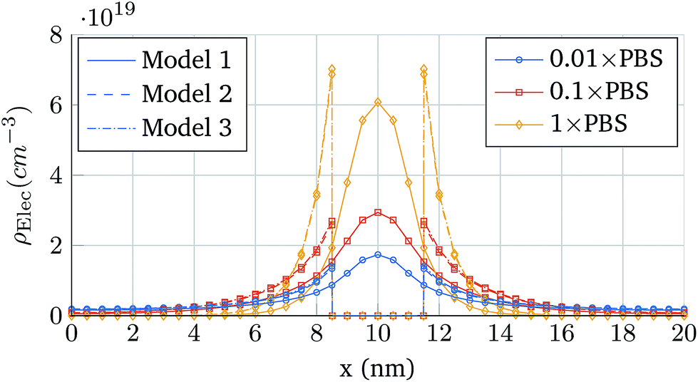 | ||
| Fig. 7 Longitudinal charge density profiles at y = 6 nm. The cases depicted correspond to the three interaction models when the PBS concentration is modified: 0.01 × PBS, 0.1 × PBS and 1 × PBS. | ||
The sensitivity of a BioFET device is determined by its capability to reproduce the molecule charges in the channel. That depends, of course, on the PBS concentration, and to what extent the molecule charge is screened by the electrolyte. In order to understand the differences between the molecular models in this regard, Fig. 8 shows the oxide contact charge (Qcont) and the electrolyte charge (Qelec) normalized to the molecular charge (QM) in the structure. Since the molecular charge is positive the changes of Qcont from negative to positive indicate that QM is completely screened and the contact associated charge only depends on Qelec.
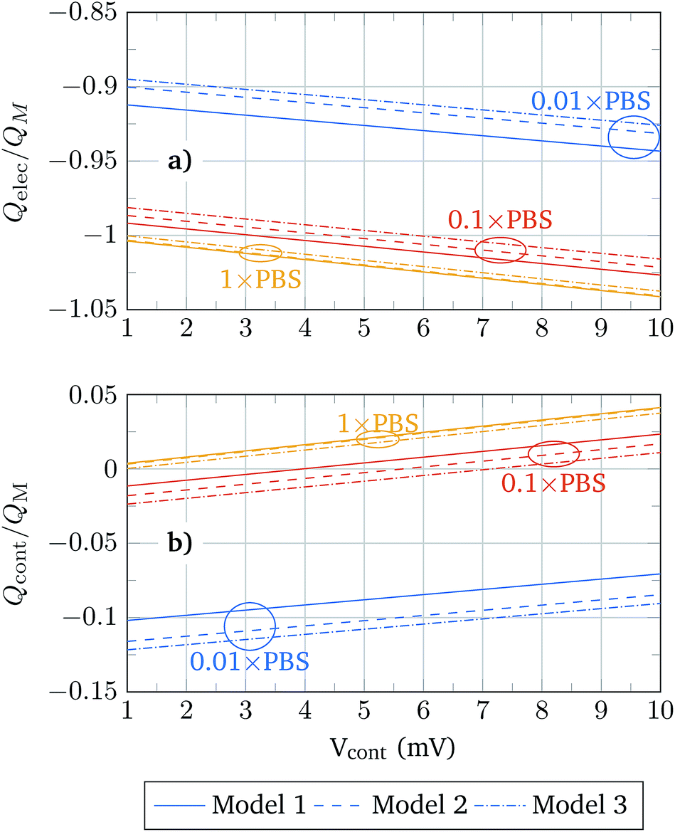 | ||
| Fig. 8 Charge density associated with the electrolyte (a) and oxide contact (b) relative to the molecule charges as a function of the oxide contact potential. The change in the sign of Qcont indicates that the molecule charge is completely screened. | ||
The relation Q/QMvs. Vcont always follows a linear trend, and the values obtained using the different models become closer as the PBS concentration is increased. For a given PBS concentration, Models 1 and 3 define the extreme values of Q/QM and Model 2 provides intermediate results that approach those of Model 1 or Model 3 depending on the PBS concentration. Thus, for low PBS concentrations, the screening is expected to be weak and the values of Model 2 are closer to those of Model 3 (solid box), while for high PBS concentrations, where a high screening takes place, Model 2 results approach the results of Model 1 (hollow boxes). This adaptability of Model 2 can be explained according to the relative role of the neutral and charged regions of the molecule under different screening conditions. In a high screening situation, the contact charge is mainly determined by the charge of the ions between the oxide interface and the molecule charged region. This neutral region is modelled in the same way in Models 1 and 2, and therefore the results obtained in both models are similar. In the weak screening case the charged region of the molecule gains relevance and Model 2 is similar to Model 3.
3.4 BioFET simulation
Finally, the complete structure is simulated. The device follows the design used in the validation against Sarkar et al.,3 but using monolayer MoS2 as a semiconductor channel, to explore the performance limit in a 2D BioFET. The electrolyte composition (0.01 × PBS) and interface traps (constant profile with 5 × 10¹⁰ eV−1 cm−2 at the SiO2–MoS2 interface and 5 × 10¹² eV−1 cm−2 at the MoS2–HfO2 interface) are the same too. Fifteen biomolecule elements are distributed uniformly over the HfO2 layer and QM is set to 200q and −200q. Two cases are analysed regarding the length of the neutral bond, hN:• First case: hN = 4 nm. The distance from the device surface to the molecular charge is lower than the Debye screening length (7.633 nm).
• Second case: hN = 20 nm. The distance from the device surface to the charged region of the molecule is higher than the Debye screening length.
In both cases the IDS − VGS response of the device is compared to the case when no molecules are attached to the device surface, IDS0. The change in the transfer characteristics is calculated as Γ = (IDS0 − IDS)/IDS0. The results of the simulations using hN = 4 nm and hN = 20 nm are depicted in Fig. 9. The most noticeable difference is observed for Model 3, where, independently of the sign of the molecule charge, the IDS response tends to be lower than the reference IDS0. This is not the case for Models 1 and 2, where the change in the sign of QM makes the output current higher or lower than IDS0. This makes sense as a negative molecule charge acts as a negative gate voltage reducing the charge density in the channel and, as a consequence, lowering the output current. The same argument can be applied to a positive QM, which acts as a positive gate voltage. In addition, the increase in hN is expected to reduce Γ to a great extent, as hN > λD.35 However, this is not the case for Model 3; in this case, Γ does not show such noticeable reduction when hN is increased from 4 nm to 20 nm, and it is even greater in the case QM > 0.
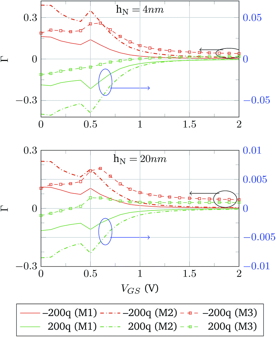 | ||
| Fig. 9 Change in the transfer curve of the device when molecules are included in the simulations. The molecular charge is set to −200q (orange) and 200q (blue) using the three interaction models. Models 1 and 2 depict a similar behaviour (quite symmetric with respect to the sign of QM and scaled down when hM increases), while Model 3 exhibits a different behaviour. | ||
Focusing on Models 1 and 2, Γ is symmetric, in the case of hN = 20 nm, to changes the sign of QM. In contrast for hN = 4 nm certain asymmetries are observed. The explanation of this behaviour comes from the differences in the modelling of the molecular charge. In the strong screening case, hN = 20 nm, the molecular charge does not have a main role in the modulation of the semiconductor charge. Then, the differences between Models 1 and 2 are translated into an increase of the magnitude of Γ. When hM is reduced to 4 nm, there is a weaker screening situation and the effect of these differences is translated into the asymmetries observed.
4 Conclusion
We have presented an extensive study of the simulation of BioFETs based on 2D materials. The implementation of a complex electrolyte model, taking into account a PBS solution and the ion pH-dependent concentration, has been demonstrated and validated against the Debye–Hückel analytical approximation, and, more importantly, against the experimental results of a MoS2 BioFET. Benefiting from the validated electrolyte description we have included different models of molecular charge interaction, evaluating their behaviour when the molecules were isolated from the semiconductor channel as well as when they were interacting with it. Noticeable differences were observed between the molecule models when testing the responsivity of the device, revealing that the molecule charge screening has a noticeable impact on the output characteristic of the device. The solid molecule model shows a particular behaviour when the polarity of the molecule is modified. In contrast, molecule models allowing a partial or total penetration of the electrolyte ions into the molecule regions exhibit a more expectable response. This is a versatile simulation approach that offers diverse and adaptable depictions of the actual molecule behaviour. The dissimilar impact of each model on the responsivity in different operating regimes can be of usefulness to better replicate and reproduce experimental results. In summary, our results provide important insights for the proper and combined modelling of molecules and the electrolyte directly contacted on the surface of 2D BioFETs, and constitute the first step on the path towards theoretical studies able to provide the experimental community with the proper design guidelines to optimize BioFETs in terms of dielectric characteristics, electrolyte composition, gate geometry, etc. These findings will be of great interest for the design of future sensor applications.Conflicts of interest
There are no conflicts of interest to declare.Acknowledgements
The authors would like to thank the financial support of Spanish Government under project TEC2017-89955-P (MINECO/AEI/FEDER,UE). A. Toral-Lopez, J. M. Gonzalez-Medina and F. J. Romero acknowledge the FPU program (FPU16/04043, FPU14/02579 and FPU16/01451). A. Toral-Lopez also acknowledges the University of Granada funding through the Becas de Inicación a la Investigación para alumnos de Máster. E. G. Marin gratefully acknowledges Juan de la Cierva incorporacion IJCI-2017-32297 (MINECO/AEI).References
- E. Stern, R. Wagner, F. J. Sigworth, R. Breaker, T. M. Fahmy and M. A. Reed, Nano Lett., 2007, 7, 3405–3409 CrossRef CAS PubMed.
- L. Wang, Y. Wang, J. I. Wong, T. Palacios, J. Kong and H. Y. Yang, Small, 2014, 10, 1101–1105 CrossRef CAS PubMed.
- D. Sarkar, W. Liu, X. Xie, A. C. Anselmo, S. Mitragotri and K. Banerjee, ACS Nano, 2014, 8, 3992–4003 CrossRef CAS PubMed.
- P. Bergveld, IEEE Trans. Biomed. Eng., 1970, BME-17, 70–71 Search PubMed.
- L. Bousse, N. D. Rooij and P. Bergveld, IEEE Trans. Electron Devices, 1983, 30, 1263–1270 Search PubMed.
- P. W. C. Clifford, D. Fung and W. H. Ko, IEEE Trans. Electron Devices, 1986, 33, 8–18 Search PubMed.
- D. Harame, L. Bousse, J. Shott and J. Meindl, IEEE Trans. Electron Devices, 1987, 34, 1700–1707 Search PubMed.
- T. Cohen-Karni, Q. Qing, Q. Li, Y. Fang and C. M. Lieber, Nano Lett., 2010, 10, 1098–1102 CrossRef CAS PubMed.
- K. S. Novoselov, Science, 2004, 306, 666–669 CrossRef CAS PubMed.
- K. S. Novoselov, D. Jiang, F. Schedin, T. J. Booth, V. V. Khotkevich, S. V. Morozov and A. K. Geim, Proc. Natl. Acad. Sci. U. S. A., 2005, 102, 10451–10453 CrossRef CAS PubMed.
- B. Lalmi, H. Oughaddou, H. Enriquez, A. Kara, S. Vizzini, B. Ealet and B. Aufray, Appl. Phys. Lett., 2010, 97, 223109 CrossRef.
- M. E. Dávila, L. Xian, S. Cahangirov, A. Rubio and G. L. Lay, New J. Phys., 2014, 16, 095002 CrossRef.
- S. Zhang, Z. Yan, Y. Li, Z. Chen and H. Zeng, Angew. Chem., Int. Ed., 2015, 54, 3112–3115 CrossRef CAS PubMed.
- J. Ji, X. Song, J. Liu, Z. Yan, C. Huo, S. Zhang, M. Su, L. Liao, W. Wang, Z. Ni, Y. Hao and H. Zeng, Nat. Commun., 2016, 7, 13352 CrossRef CAS PubMed.
- L. H. Hess, C. Becker-Freyseng, M. S. Wismer, B. M. Blaschke, M. Lottner, F. Rolf, M. Seifert and J. A. Garrido, Small, 2014, 11, 1703–1710 CrossRef PubMed.
- J. Lee, P. Dak, Y. Lee, H. Park, W. Choi, M. A. Alam and S. Kim, Sci. Rep., 2014, 4, 7352 CrossRef CAS PubMed.
- H. Nam, B.-R. Oh, M. Chen, S. Wi, D. Li, K. Kurabayashi and X. Liang, J. Vac. Sci. Technol., B: Nanotechnol. Microelectron.: Mater., Process., Meas., Phenom., 2015, 33, 06FG01 Search PubMed.
- H. Nam, B.-R. Oh, P. Chen, M. Chen, S. Wi, W. Wan, K. Kurabayashi and X. Liang, Sci. Rep., 2015, 5, 10546 CrossRef PubMed.
- B. Ryu, E. Yang, Y. Park, K. Kurabayashi and X. Liang, J. Vac. Sci. Technol., B: Nanotechnol. Microelectron.: Mater., Process., Meas., Phenom., 2017, 35, 06G805 Search PubMed.
- I.-Y. Chung, H. Jang, J. Lee, H. Moon, S. M. Seo and D. H. Kim, Nanotechnology, 2012, 23, 065202 CrossRef PubMed.
- D. Passeri, A. Morozzi, K. Kanxheri and A. Scorzoni, Biomed. Eng. Online, 2015, 14, S3 CrossRef PubMed.
- F. Pittino, P. Palestri, P. Scarbolo, D. Esseni and L. Selmi, Solid-State Electron., 2014, 98, 63–69 CrossRef CAS.
- A. Bandiziol, P. Palestri, F. Pittino, D. Esseni and L. Selmi, IEEE Trans. Electron Devices, 2015, 62, 3379–3386 CAS.
- T. Windbacher, V. Sverdlov, S. Selberherr, C. Heitzinger, N. Mauser and C. Ringhofer, 2008, International Conference on Simulation of Semiconductor Processes and Devices, 2008 Search PubMed.
- X. Yang, W. R. Frensley, D. Zhou and W. Hu, IEEE Trans. Nanotechnol., 2012, 11, 501–512 Search PubMed.
- C. Heitzinger, R. Kennell, G. Klimeck, N. Mauser, M. McLennan and C. Ringhofer, J. Phys.: Conf. Ser., 2008, 107, 012004 CrossRef.
- H. Nam, B.-R. Oh, P. Chen, J. S. Yoon, S. Wi, M. Chen, K. Kurabayashi and X. Liang, Appl. Phys. Lett., 2015, 107, 012105 CrossRef.
- A. Kakatkar, T. S. Abhilash, R. D. Alba, J. M. Parpia and H. G. Craighead, Nanotechnology, 2015, 26, 125502 CrossRef PubMed.
- B. Cai, S. Wang, L. Huang, Y. Ning, Z. Zhang and G.-J. Zhang, ACS Nano, 2014, 8, 2632–2638 CrossRef CAS PubMed.
- D.-J. Kim, I. Y. Sohn, J.-H. Jung, O. J. Yoon, N.-E. Lee and J.-S. Park, Biosens. Bioelectron., 2013, 41, 621–626 CrossRef CAS PubMed.
- B. Ryu, H. Nam, B.-R. Oh, Y. Song, P. Chen, Y. Park, W. Wan, K. Kurabayashi and X. Liang, ACS Sens., 2017, 2, 274–281 CrossRef CAS PubMed.
- M. W. Shinwari, M. J. Deen and D. Landheer, Microelectron. Reliab., 2007, 47, 2025–2057 CrossRef.
- S. Birner, Ph.D. thesis, Technische Universität München, 2011.
- D. Landheer, W. R. McKinnon, G. Aers, W. Jiang, M. J. Deen and M. W. Shinwari, IEEE Sens. J., 2007, 7, 1233–1242 CAS.
- A. Poghossian, A. Cherstvy, S. Ingebrandt, A. Offenhäusser and M. Schöning, Sens. Actuators, B, 2005, 111–112, 470–480 CrossRef CAS.
- W. R. McKinnon and D. Landheer, J. Appl. Phys., 2006, 100, 054703 CrossRef.
Footnote |
| † Pervasive Electronics Advanced Research Laboratory. |
| This journal is © The Royal Society of Chemistry 2019 |