
 Open Access Article
 This Open Access Article is licensed under a
 Creative Commons Attribution 3.0 Unported Licence
Molecular spectroscopy in a solid-state device†
Ainhoa
Atxabal
 a,
Thorsten
Arnold
b,
Subir
Parui
c,
Elisabetta
Zuccatti
a,
Mirko
Cinchetti
d,
Fèlix
Casanova
ae,
Frank
Ortmann
b and
Luis E.
Hueso
*ae
a,
Thorsten
Arnold
b,
Subir
Parui
c,
Elisabetta
Zuccatti
a,
Mirko
Cinchetti
d,
Fèlix
Casanova
ae,
Frank
Ortmann
b and
Luis E.
Hueso
*ae
aCIC nanoGUNE, 20018 Donostia-San Sebastian, Basque Country, Spain. E-mail: l.hueso@nanogune.eu
bCenter for Advancing Electronics Dresden, Technische Universität Dresden, 01062 Dresden, Germany
cIMEC and K. U. Leuven, 3001 Leuven, Belgium
dExperimentelle Physik VI, Technische Universität Dortmund, Dortmund 44221, Germany
eIKERBASQUE, Basque Foundation for Science, 48013 Bilbao, Basque Country, Spain
First published on 7th May 2019
Abstract
The quantification of the electronic transport energy gap of a molecular semiconductor is essential for pursuing any challenge in molecular optoelectronics. However, this remains largely elusive because of the difficulties in its determination by conventional spectroscopic methods. This communication presents an in-device molecular spectroscopy (i-MOS) technique, which permits measuring this gap seamlessly, in real device operative conditions, at room temperature and without any previous knowledge of the material's parameters. This result is achieved by determining the occupied and unoccupied molecular orbitals of an organic semiconductor thin-film by using a single three terminal solid-state device.
New conceptsIn this manuscript we are able to determine the transport energy gap of a molecular semiconductor under in-operando conditions and without any prior knowledge of material parameters. The measurements have been performed at room temperature with a three terminal vertical solid-state device, which makes this technique convenient for and related to opto-electronic device applications. In spite of its relevance, the reality is that so far there is not an experimental or computational technique capable of delivering such value without approximations involved. The vast community working in organic electronics has simply adjusted to work with substitutes, such as the energy gap values obtained by UV-VIS or photoemission spectroscopy techniques. The value of the transport gap of the organic semiconductor determines, for example and in a first approximation, the conductivity of a material and its possible integration in commercial devices. Here we demonstrate a novel, simple and accurate way for obtaining the transport gap; a value that cannot be obtained with the current experimental or theoretical approaches. |
The engineering of molecular semiconductor-based technologies requires precise knowledge of key parameters, such as the relative energetic position of the molecular levels and proper quantification of the transport energy gap.1–6 However, the lack of a reliable and straightforward technique for the determination of the transport energy gap in the bulk of an organic semiconductor often results in the adoption of inadequate substitutes, such as the single-molecular fundamental, Kohn–Sham, electrochemical, optical or interface gaps.7 The single-molecular fundamental gap, obtained by single-molecule scanning tunneling spectroscopy,8,9 cannot be interpreted as a transport gap, because the strong polarization coming from the π-conjugated molecules makes the transport gap different from the energy gap at the single molecule level.7,10–12 The use of the Kohn–Sham gap from density functional theory on the other hand has no formal justification and is thus dependent on cancelation of intrinsic errors and inadequacies present in this method.7 On the other hand, the electrochemical gap is principally related to reduction–oxidation potentials, which can be sensitive to solvation and Coulombic effects.13,14 In addition, the optical gap, commonly measured by ultraviolet-visible spectroscopy (UV-VIS), is different from the transport gap due to the strong exciton binding energy of molecules.7,13,15–17 Besides, in the case of some organic semiconductors such as C60 fullerenes, the optical transition associated with the transport states may be symmetry forbidden, which leads to UV-VIS possibly measuring higher onset energies. Finally, the interface gap, obtained by a combination of different surface-sensitive techniques, typically ultraviolet photoemission spectroscopy (UPS) and inverse photoemission spectroscopy (IPES),18–20 can be used to estimate the transport gap, but under the careful consideration of different limiting factors, such as the low resolution of IPES (0.4 eV), the probing depth at the organic-vacuum interface and other surface dependent parameters like roughness.21
In this work, thanks to an in-device molecular spectroscopy (i-MOS) technique, we are able to determine directly in-operando both the energetic positions of the highest occupied molecular orbital (HOMO) states and the lowest unoccupied molecular orbital (LUMO) states and the transport energy gap of a molecular semiconductor. This has been accomplished by using a three-terminal solid-state device and without any pre-knowledge of the material parameters. As proof of principle we have chosen C60 and C70, two well established molecular semiconductors in the field of electronics and optoelectronics.22–27 Moreover, the similar chemical structure and the consequent close molecular orbital energies of both materials permit us to test the sensitivity of i-MOS.
i-MOS is performed in a three-terminal vertical device, which is composed of an aluminium/aluminium oxide emitter (E), a gold (Au) base (B) and an n-type organic semiconductor (C60 and C70) collector with an aluminium top contact (C) (see Fig. 1).21 Details on the device fabrication and thin film characterization can be found in the Methods section [device cross section and top view are shown in ESI,† Fig. S1. Atomic force microscopy and X-ray diffraction measurements are shown in ESI,† Fig. S2 and S3, respectively, while a basic electrical characterization of the device is available in ESI,† Fig. S4 and S5]. We should highlight the simple fabrication method, which should be available to many groups working in the field of organic optoelectronics. Fig. 1 shows the working principle of i-MOS. When a negative emitter base bias, VEB, is applied, a current IE is injected from the emitter into the base by tunnelling through the Al2O3 barrier. These electrons are “hot” in the base as their energy is well above (≫kBT) the Fermi level of the metal, and a small fraction of them crosses the thin metallic base ballistically without any significant energy attenuation.11,28–30 For the case in which the applied bias −eVEB ≥ Δ (Δ is the metal–semiconductor energy barrier), some of the injected hot electrons enter into the LUMO states, while the remaining ones flow back into the base. At higher energies, electrons can also enter into higher energy conductive states, such as LUMO+1 states. Since C60 and C70 are n-type semiconductors and they are sandwiched between two metallic contacts with different work functions, the emerging built-in potential enables the detection of the electron current, IC, without any applied collector-base bias, VCB (Fig. 1a).31,32 Under a negative applied VCB (Fig. 1c), the electric field in the base-collector junction repulses hot electrons and leads to the detection of holes injected into the HOMO level of the n-type semiconductor, thus enabling the determination of the relative energy of that molecular level with respect to EF of the base metal. These holes are created by the inelastic scattering of the incident hot electrons in the gold metal base with cold electrons (below the Fermi level).33–35 A similar mechanism operates for positive VEB, but in this case holes are injected into the base, instead of electrons. Fig. 1b represents an Auger-like scattering process in which incident holes excite secondary electron–hole pairs in the gold metal base and thus hot electrons are created.36–38Fig. 1d shows the direct process of hole-injection and hole-detection, respectively.
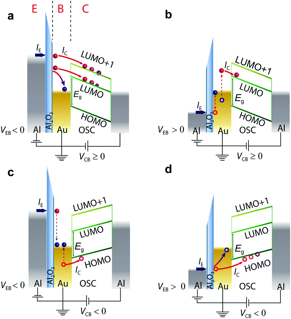 | ||
| Fig. 1 In-device molecular spectroscopy (i-MOS) operation under different emitter-base bias VEB polarities at room temperature. (a) Schematic representation of the direct process in which electrons are injected by applying a negative emitter-base bias, VEB < 0 V, and detected in the molecular semiconductor. The measurements can be performed either without any externally applied base collector bias, VCB, or by VCB ≥ 0 V. (b) Schematic representation of the secondary process at i-MOS when holes are injected into the device, VEB > 0 V, but hot electrons coming from a similar effect to Auger scattering are detected with VCB ≥ 0 V. (c) Schematic representation of the secondary process at i-MOS when electrons are injected, VEB < 0 V, into the device but holes are detected. VCB < 0 V is required in order to cancel the built-in potential and help hole injection into and transport through the organic semiconductor. (d) Schematic representation of the direct process at i-MOS when holes are injected, VEB > 0 V, and detected with VCB < 0 V. | ||
Fig. 2 reports the experimental values of the collector current, IC, with VEB of C60-based i-MOS, measured under the operations described in Fig. 1. Fig. 2a shows the direct electron process, i.e. electron injection and electron detection, when VEB < 0 V and VCB = 0 V is applied. Fig. 2a also shows the derivative of the IC, |dIC/dV|. Two onsets are observed in the |dIC/dV| curve, which corresponds to the selection of the molecular orbital levels, in this case LUMO at 0.8 ± 0.1 eV and LUMO+1 at 1.7 ± 0.1 eV. The energies of the molecular orbital levels extracted with i-MOS are relative to the Fermi energy of the gold base. The relative energy of the LUMO level is consistent with the energy value acquired for the same molecular level by secondary hole–electron processes when VEB > 0 V and VCB = 0 V (see Fig. 2b). The |dIC/dV| curve of this plot shows the onset of the LUMO at 0.9 ± 0.1 eV. Fig. 2c and d show the IC and |dIC/dV| versus VEB for secondary electron–hole and direct hole processes. In both figures an onset is observed at the |dIC/dV| curves, which corresponds to the relative energy of the HOMO level at 1.6 ± 0.1 eV. The direct hole process has been achieved by VEB > 0 V and VCB = −0.5 V, while the secondary electron–hole process by VEB < 0 V and VCB = −0.5 V. Playing with the freedom that the collector electrode offers us, we tune the built-in potential of the organic semiconductor by the VCB, which permits choice of the carrier type (electrons or holes) responsible for the transport in the organic semiconductor-based device. ESI,† Fig. S6–S9 show a detailed VCB dependence of C60 i-MOS.
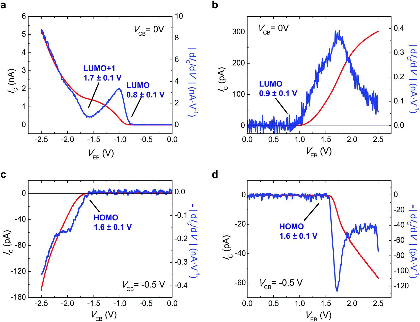 | ||
| Fig. 2 In-device molecular spectroscopy (i-MOS) of C60 fullerene performed at different emitter-base bias VEB polarities. (a) Collector current IC for negative emitter base bias VEB < 0 V (red solid line) and its derivative with respect to VEB (blue solid line) at 300 K. Energetic electrons are injected with VCB = 0 V both into the lowest molecular orbital (LUMO) and into the next higher excited conductive molecular level (LUMO+1) states of C60. Note that in the current configuration, positive IC indicates electron current detection whereas negative IC corresponds to hole current detection in C60. (b) Electron current, IC, and LUMO states detected with VEB > 0 V and VCB = 0 V (red solid line) together with the derivative of the IC with respect to VEB (blue solid line) at 300 K. (c) Detected IC for VEB < 0 V and VCB = −0.5 V (red solid line) and the derivative of the IC with respect to VEB (blue solid line) at room temperature, 300 K. Injection of a hole current into C60 leads to the detection of its highest occupied molecular orbital (HOMO) states. (d) ICversus VEB when VEB > 0 V and VCB = −0.5 V (red solid line), and the derivative of the IC with respect to VEB (blue solid line). Injection of hot holes permits the detection of the HOMO states of C60 in a direct process. | ||
In order to extend our approach to another compound, in Fig. 3 we study the i-MOS operations described in Fig. 1 for C70-based i-MOS devices. C70 is a larger n-type buckyball than C60, which permitted us to test the sensitivity and energy resolution of i-MOS for systems with similar energetic structure. In the case of C70-based i-MOS, we could determine that the relative energy of the LUMO with respect to the Fermi level of gold is 0.7 ± 0.1 eV, the one of LUMO+1 is 1.6 ± 0.1 eV (Fig. 3a and b) and the HOMO level of C70 is at 1.5 ± 0.1 eV below the Fermi level of the base metal (Fig. 3c and d). The values extracted from direct processes and secondary processes are in agreement. ESI,† Fig. S10–S13 show a detailed VCB dependence of C70 i-MOS. All these energy levels are summarized in Fig. 4.
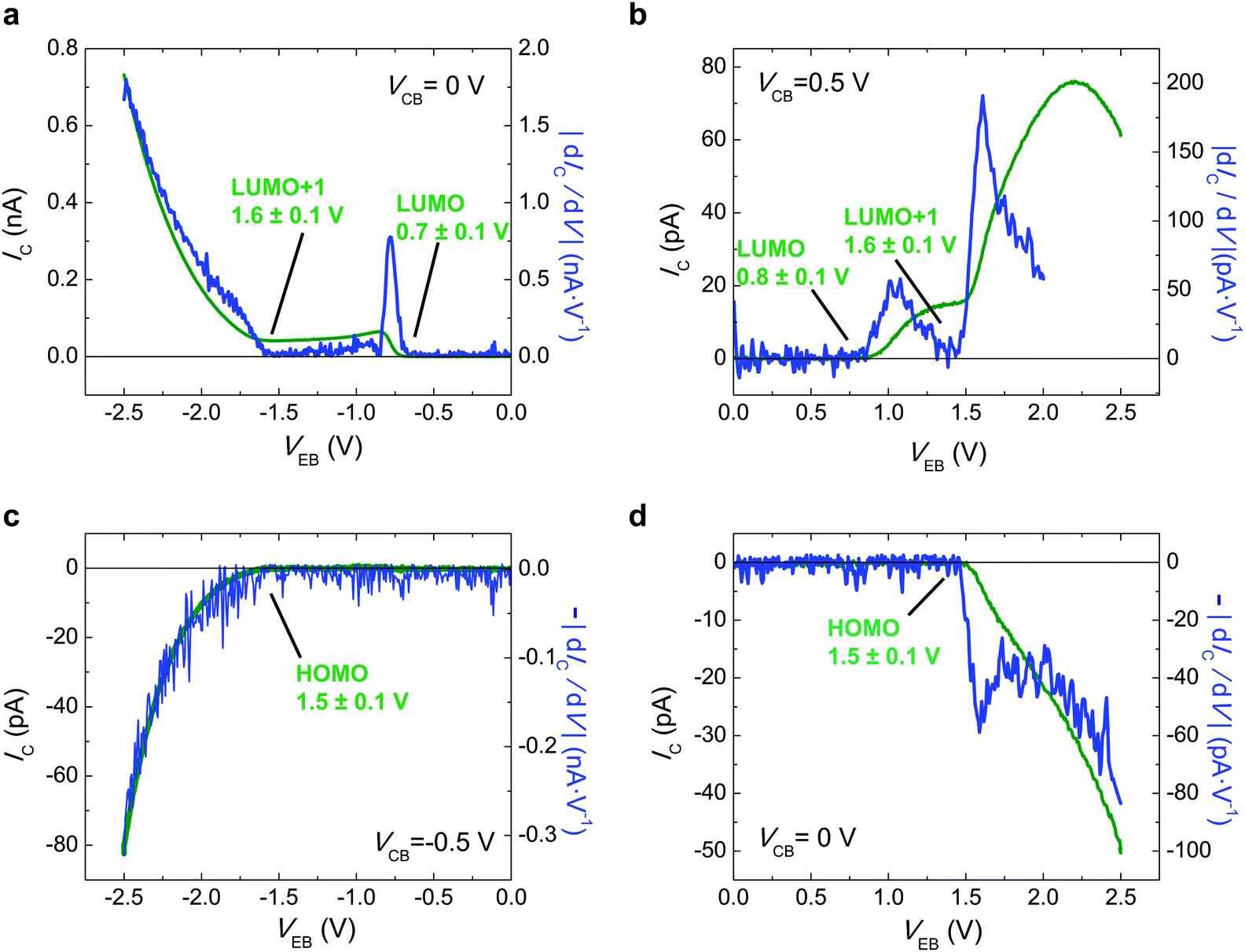 | ||
| Fig. 3 In-device molecular spectroscopy (i-MOS) operation for C70 fullerene under different emitter-base bias VEB polarities. (a) Collector current IC for negative emitter base bias VEB < 0 V (green solid line) and its derivative with respect to VEB (blue solid line) at 200 K. Energetic electrons are injected with VCB = 0 V both into the lowest molecular orbital (LUMO) and into the next higher excited conductive molecular level (LUMO+1) states of C70. Note that in the current configuration, positive IC indicates electron current detection whereas negative IC corresponds to hole current detection in C70. (b) Electron current, IC, and LUMO and LUMO+1 states detected with VEB > 0 V and VCB = 0.5 V (green solid line) together with the derivative of IC with respect to VEB (blue solid line) at 200 K. (c) Detected IC for VEB < 0 V and VCB = −0.5 V (green solid line) and the derivative of the IC with respect to VEB (blue solid line) at 200 K. Injection of a hole current into C70 leads to the detection of its highest occupied molecular orbital (HOMO) states. (d) ICversus VEB when VEB > 0 V and VCB = −0.5 V (green solid line), and the derivative of the IC with respect to VEB (blue solid line). Injection of energetic holes permits the detection of the HOMO states of C70 in a direct process. | ||
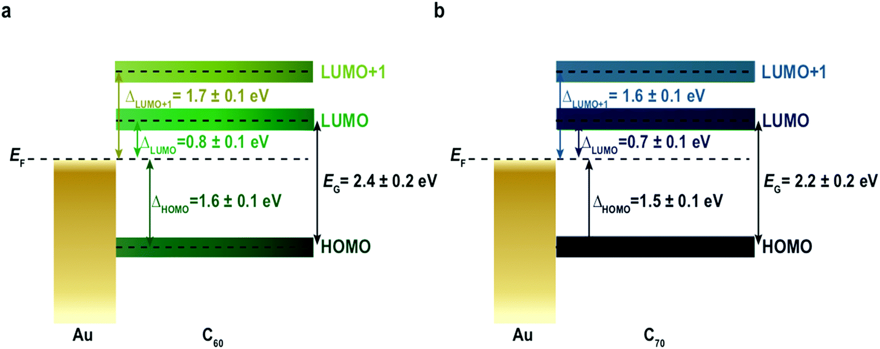 | ||
| Fig. 4 Au/C60 and Au/C70 energy level alignment. EF is the Fermi energy of gold. The LUMO corresponds to the lowest unoccupied molecular orbital and LUMO+1 to the next higher excited conductive molecular orbitals, respectively, and HOMO to the highest occupied molecular orbital. EG is the energy gap between HOMO and LUMO of (a) C60 and (b) C70Δ corresponds to the energy barrier between the Fermi energy of gold and the molecular level devoted to charge transport. The sublabel of each Δ refers to its corresponding molecular orbital. | ||
The transport gap of both C60 and C70 in real device operative conditions can be simply calculated taking into account the energetic difference between the HOMO and LUMO levels, leading to a value of 2.4 ± 0.2 eV in the case of C60 (Fig. 4a) and 2.2 ± 0.2 eV in the case of C70 (Fig. 4b), when averaged over dozens of devices (ESI,† Table S1). This quantity is obtained without any assumption regarding the nature of the molecular material, and hence the method presented is easily transferred to other systems under study. The difference detected in the transport gap between C60 and C70 proves the sensitivity of i-MOS. The carrier transport gap is a key parameter for many (opto)electronic applications1–6,39 and there are currently several other techniques routinely used to approach this quantity indirectly,7 including electrochemical spectroscopy,13,14 ultraviolet-visible spectroscopy (UV-VIS),15–17 ultraviolet photoemission spectroscopy (UPS), inverse photoemission spectroscopy (IPES),18–20,40 and single-molecule scanning tunnelling spectroscopy.8,10 ESI,† Table S2 compares the EG of C60 on gold extracted by several different methods. In our case, we can determine directly and without any prior assumptions, both the relative energetic positions of the HOMO and LUMO states, and the transport energy gap of a molecular semiconductor in real operative conditions and at room temperature.
Conclusions
In conclusion, by making use of the i-MOS technique we report an unprecedented full energy characterization of both hole and electron transport levels of molecular semiconductors under in-operando conditions. This information cannot be obtained by any other experimental technique, while it is paramount for the understanding and development of any future complex molecule-based (opto)electronic devices. Moreover, we have shown that i-MOS is able to detect small energy differences in the energy level alignment of similar molecules such as C60 and C70. The results reported in this work present a reliable, direct and easily applicable device-spectroscopic method. This makes it a promising technique for studies on the injection properties of metal–organic interfaces as well as the manipulation of the electronic transport states of organic semiconductors, for instance by doping. Since the knowledge of the electronic levels and its optimization are crucial to improve the efficiency of virtually all optoelectronic devices, we expect i-MOS in the future to provide accurate energies and new insights which are at the root of new developments.Methods
Device fabrication
All the devices described in this work were fabricated in situ in an ultra high vacuum (UHV) multi chamber evaporator (base pressure <10−9 mbar) with a shadow mask system. The emitter is a 12 nm-thick aluminium contact, 99.95% purity (Lesker), which was thermally evaporated in an effusion cell with a rate of 0.6 Å s−1. A crucible of pyrolytic boron nitride (PBN) was used. The Al2O3 tunnel junction was made by plasma oxidizing the aluminium contact, first for two minutes at low power (1200 V and 10 mA at 0.1 mbar) and then for three minutes at high power (1200 V and 50 mA at 0.1 mbar). A 10 nm-thick gold base (99.95% purity, Lesker) was e-beam evaporated from a vitreous-coated graphite-based crucible, and used as a base contact. The evaporation rate was 1.0 Å s−1. C60 (and C70) triple-sublimed quality (99.9%, Sigma Aldrich), was thermally evaporated in a quartz-based crucible with a rate of 0.1 Å s−1. Finally, a 12 nm-thick aluminium top electrode was again thermally evaporated. A two-step deposition (2 nm at 0.1 Å s−1 and 10 nm at 0.6 Å s−1) was followed in order to minimize the damage to the organic film.The sample size is 10 × 10 mm2, and six devices were produced with every sample.
Electrical characterization
Electrical characterization was performed under high vacuum (base pressure 5 × 10⁻⁵ mbar) in a variable-temperature probe-station (Lakeshore). A Keithley 4200 semiconductor analyser system was used to record I–V curves.Conflicts of interest
There are no conflicts to declare.Acknowledgements
The authors acknowledge Prof. Francesca Tinti for her critical opinion about the manuscript. This work is supported by the European Research Council (Grants 257654-SPINTROS and 725767-hyControl), by the Spanish MINECO under Project No. MAT2015-65159-R and Maria de Maeztu Units of Excellence Program – MDM-2016-0618 and by the Basque Government (under Project No. PC2015-1-01). A. A. acknowledges the Basque Government for a PhD fellowship (PRE_2017_2_0052). The work at TU Dresden was supported by the Deutsche Forschungsgemeinschaft (Grant OR 349/1-1). Grants for computing time from the Centre for Information Services and High Performance Computing of TU Dresden are gratefully acknowledged.References
- M. Schwarze, W. Tress, B. Beyer, F. Gao, R. Scholz, C. Poelking, K. Ortstein, A. A. Günther, D. Kasemann, D. Andrienko and K. Leo, Science, 2016, 352, 1446 CrossRef CAS PubMed.
- S. Holliday, R. S. Ashraf, A. Wadsworth, D. Baran, S. A. Yousaf, C. B. Nielsen, C.-H. Tan, S. D. Dimitrov, Z. Shang, N. Gasparini, M. Alamoudi, F. Laquai, C. J. Brabec, A. Salleo, J. R. Durrant and I. McCulloch, Nat. Commun., 2016, 7, 11585 CrossRef CAS PubMed.
- J. Lee, H.-F. Chen, T. Batagoda, C. Coburn, P. I. Djurovich, M. E. Thompson and S. R. Forrest, Nat. Mater., 2015, 15, 92 CrossRef PubMed.
- M. Muccini, Nat. Mater., 2006, 5, 605 CrossRef CAS PubMed.
- S. R. Forrest, Nature, 2004, 428, 911 CrossRef CAS PubMed.
- X. Sun, S. Vélez, A. Atxabal, A. Bedoya-Pinto, S. Parui, X. Zhu, R. Llopis, F. Casanova and L. E. Hueso, Science, 2017, 357, 677 CrossRef CAS PubMed.
- J. L. Bredas, Mater. Horiz., 2014, 1, 17 RSC.
- A. Nitzan and M. A. Ratner, Science, 2003, 300, 1384 CrossRef CAS PubMed.
- A. Bannani, C. Bobisch and R. Moller, Science, 2007, 315, 1824 CrossRef CAS PubMed.
- S. F. Alvarado, P. F. Seidler, D. G. Lidzey and D. D. C. Bradley, Phys. Rev. Lett., 1998, 81, 1082 CrossRef CAS.
- M. Jung, D. Shin, S.-D. Sohn, S.-Y. Kwon, N. Park and H.-J. Shin, Nanoscale, 2014, 6, 11835 RSC.
- C. Gaul, S. Hutsch, M. Schwarze, K. S. Schellhammer, F. Bussolotti, S. Kera, G. Cuniberti, K. Leo and F. Ortmann, Nat. Mater., 2018, 17, 439 CrossRef CAS PubMed.
- R. Holze, Organometallics, 2014, 33, 503 CrossRef.
- V. Nádazdy, F. Schauer and K. Gmucová, Appl. Phys. Lett., 2014, 105, 142109 CrossRef.
- D. A. Evans, A. R. Vearey-Roberts, O. R. Roberts, G. T. Williams, S. P. Cooil, D. P. Langstaff, G. Cabailh, I. T. McGovern and J. P. Goss, J. Appl. Phys., 2013, 114, 123701 CrossRef.
- B. A. Gregg and M. C. Hanna, J. Appl. Phys., 2003, 93, 3605 CrossRef CAS.
- A. Kahn, Mater. Horiz., 2016, 3, 7 RSC.
- B. S. Braun, W. R. Salaneck and M. Fahlman, Adv. Mater., 2009, 21, 1450 CrossRef.
- E. L. Shirley and S. G. Louie, Phys. Rev. Lett., 1993, 71, 133 CrossRef CAS PubMed.
- J. Hwang, A. Wan and A. Kahn, Mater. Sci. Eng., R, 2009, 64, 1 CrossRef.
- A. Atxabal, S. Braun, T. Arnold, X. Sun, S. Parui, X. Liu, C. Gozalvez, R. Llopis, A. Mateo-Alonso, F. Casanova, F. Ortmann, M. Fahlman and L. E. Hueso, Adv. Mater., 2017, 10, 1606901 CrossRef PubMed.
- X. Wang, E. Perzon, F. Oswald, F. Langa, S. Admassie, M. R. Andersson and O. Inganäs, Adv. Funct. Mater., 2005, 15, 1665 CrossRef CAS.
- K. Schulze, C. Uhrich, R. Schüppel, K. Leo, M. Pfeiffer, E. Brier, E. Reinold and P. Bäuerle, Adv. Mater., 2006, 18, 2872 CrossRef CAS.
- D. M. Guldi and N. Martin, Fullerenes: From Synthesis to Optoelectronic Properties, Springer, Netherlands, 2002 Search PubMed.
- G. A. Salvatore, N. Mu, T. Kinkeldei, L. Petti, C. Zysset, G. Tro, I. Strebel and L. Bu, Nat. Commun., 2014, 5, 2982 CrossRef PubMed.
- M. P. Klinger, A. Fischer, F. Kaschura, R. Scholz, B. Lüssem, B. Kheradmand-Boroujeni, F. Ellinger, D. Kasemann and K. Leo, Adv. Mater., 2015, 27, 7734 CrossRef CAS PubMed.
- T. D. Anthopoulos, B. Singh, N. Marjanovic, N. S. Sariciftci, A. Montaigne Ramil, H. Sitter, M. Cölle and D. M. De Leeuw, Appl. Phys. Lett., 2006, 89, 7 CrossRef.
- M. Gobbi, L. Pietrobon, A. Atxabal, A. Bedoya-Pinto, X. Sun, F. Golmar, R. Llopis, F. Casanova and L. E. Hueso, Nat. Commun., 2014, 5, 4161 CrossRef CAS PubMed.
- N. Balkan, Hot Electrons Semicond., Clarendon Press, Oxford, 1998, pp. 385–427 Search PubMed.
- T. Arnold, A. Atxabal, S. Parui, L. E. Hueso and F. Ortmann, Adv. Funct. Mater., 2018, 20, 1706105 CrossRef.
- W. J. Kaiser and L. D. Bell, Phys. Rev. Lett., 1988, 60, 1406 CrossRef CAS PubMed.
- L. D. Bell and W. J. Kaiser, Phys. Rev. Lett., 1988, 61, 2368 CrossRef CAS PubMed.
- M. Bauer, A. Marienfeld and M. Aeschlimann, Prog. Surf. Sci., 2015, 90, 319 CrossRef CAS.
- T. Banerjee, E. Haq, M. H. Siekman, J. C. Lodder and R. Jansen, IEEE Trans. Magn., 2005, 41, 2642 Search PubMed.
- B. G. Park, E. Haq, T. Banerjee, B. C. Min, J. C. Lodder and R. Jansen, J. Appl. Phys., 2006, 99, 08S701 CrossRef.
- W. Yi, V. Narayanamurti, H. Lu, M. A. Scarpulla and A. C. Gossard, Phys. Rev. B: Condens. Matter Mater. Phys., 2010, 81, 235325 CrossRef.
- W. Yi, V. Narayanamurti, H. Lu, M. A. Scarpulla, A. C. Gossard, Y. Huang, J. H. Ryou and R. D. Dupuis, Appl. Phys. Lett., 2009, 95, 112102 CrossRef.
- L. D. Bell, J. Vac. Sci. Technol., B: Microelectron. Nanometer Struct.–Process., Meas., Phenom., 1991, 9, 594 CrossRef.
- M. Cinchetti, V. A. Dediu and L. E. Hueso, Nat. Mater., 2017, 16, 507 CrossRef CAS PubMed.
- H. Yoshida, Chem. Phys. Lett., 2012, 53, 180 CrossRef.
Footnote |
| † Electronic supplementary information (ESI) available. See DOI: 10.1039/c9mh00218a |
| This journal is © The Royal Society of Chemistry 2019 |