
Growth of a dense gadolinium metal–organic framework on oxide-free silicon for cryogenic local refrigeration†
Giulia
Lorusso
 ,
Eva
Natividad
,
Marco
Evangelisti
and
Olivier
Roubeau
*
,
Eva
Natividad
,
Marco
Evangelisti
and
Olivier
Roubeau
*
Instituto de Ciencia de Materiales de Aragón (ICMA), CSIC and Universidad de Zaragoza, Pedro Cerbuna 12, 50009 Zaragoza, Spain. E-mail: roubeau@unizar.es
First published on 17th October 2018
Abstract
Certain magnetic molecules and molecular-based frameworks are considered as alternative materials for cryogenic cooling due to their large magneto-caloric effect. This potential is particularly appealing for applications requiring local refrigeration, but so far no study has been aimed at making thin films of efficient molecular coolers on a typical device substrate and evaluating their cooling potential. In this work, the growth of a dense gadolinium metal–organic framework on oxide-free silicon covered by either self-assembled or covalent monolayers with carboxylic end groups is explored. A continuous coverage with nanosized crystallites of the selected gadolinium formate framework is successfully formed on covalent monolayers obtained by hydrosilylation with either undecenoic acid or undecynoic acid. The thickness of the magnetocaloric deposit can be increased by increasing the growth time, as shown by the surface densities derived through determination of the film magnetic properties. An estimation of the cooling potential of the thicker film obtained shows that it would refrigerate a 2 μm thick Si membrane from 5 to 0.8 K, by adiabatic demagnetization from 2 T to zero field. Altogether, this study demonstrates the potential of molecular cooler thin films to develop on-chip magnetic refrigeration at cryogenic temperatures.
Conceptual insightsWe present a method to provide solid-state devices with in situ cooling potential for low temperatures, through the formation of a thin layer of an adequate metal–organic framework material. Gadolinium molecular-based materials have arisen as alternative coolants in magnetic refrigeration applications, which rely on the magnetocaloric effect of paramagnetic solids. This is particularly true for situations in which their relatively low thermal conductivity is not detrimental, i.e. for application requiring local cooling. Surprisingly, there has been no study aimed as yet at making thin films of efficient molecular magnetic coolers on typical substrates used in electronic device elaboration. The strategy used in this work allows the formation on oxide-free silicon of a continuous layer of crystallites of gadolinium formate, one of the best molecular-based coolers due to its high relative density of magnetic elements. Estimation of the cooling potential of the deposit demonstrates that silicon membranes would be efficiently cooled from 5 K to sub-Kelvin temperatures by a single adiabatic demagnetization, surpassing the electronic schemes currently used for such local cooling, and therefore validating the proposed approach. |
1. Introduction
Molecular nanomagnets are a class of materials based on isolated coordination complexes composed of one to numerous interacting paramagnetic metal ions. Their peculiar magnetic properties at the molecular scale have resulted in their proposed use in various applications including (quantum) information storage and processing,1 spin-based quantum computing2 and cryogenic refrigeration.3 The latter relies on materials with a large magneto-caloric effect (MCE),4i.e., important changes of the magnetic entropy ΔSm and adiabatic temperature ΔTad associated with a change in the applied magnetic field ΔB. Adiabatic demagnetization refrigerators typically use oxides, such as gadolinium gallium garnet (GGG), and inorganic paramagnetic salts, such as cerium magnesium nitrate (CMN) or chromic potassium alum (CPA), to allow cooling to respectively liquid-helium temperatures and ultra-low temperatures, being valid alternatives to the use of liquid-helium itself or to 3He–4He dilution fridges.5 Although the currently used materials are well suited and developed,6 molecular-based materials have been proposed as alternatives on the basis of the possibilities offered by molecular-scale rational synthetic design.3 Indeed, minimizing anisotropy and maximizing the density of spin carriers, while avoiding long-range magnetic order, has brought the MCE of molecular-based systems to values competing with the currently used materials.7,8 Unfortunately, their use in bulk applications might be severely hampered by the low thermal conductivity that can be expected from their molecular nature, an aspect that has remained somewhat underscored while these so-called molecular coolers have been arousing increased interest.9 We have recently reported the first evaluation of the cryogenic thermal conductivity of an archetypal molecular cooler, [Gd2(OAc)6(H2O)4]·4H2O, confirming this important limitation.10 We have also evaluated the relative improvement that can be obtained through the elaboration of composite materials with a component with good thermal conductivity,10 although the gain remained limited. Nevertheless, direct measurements of the MCE of samples of different thicknesses have also shown that thinner samples or layers are not affected by the adverse effects of the poor thermal conductivity of the material.10 Basically, a sufficiently reduced thickness makes negligible temperature gradients within the material in contact with a thermal bath, a consequence of its poor thermal conductivity. This in turn minimizes any related loss of cooling potential. A low thermal conductivity may therefore not represent such a stringent limitation if the molecular cooler is to refrigerate locally, for example, as a coating on a membrane. Under such conditions, even if the thermal conductance at the interface will still play a role, the molecular cooler should be able to efficiently cool the material it is in contact with. Here, molecular materials possess an advantage in that they may be processed in solution, and therefore assembled and integrated directly on the surface to be cooled. Such ability has been demonstrated, and the large MCE of the molecular materials shown to be maintained in their deposits.11,12 A strategy using membranes coated with molecular coolers as local micro-refrigerators would have a significant interest in any application requiring local, fast and light refrigeration, for example, in sensors used in space borne missions (Scheme 1 left).13 For such objective, the choice of the substrate is imposed by the necessity of a low heat capacity, combined with easy manipulation and good thermal conductivity. Among typical substrates used in device fabrication, Si is clearly the one with the lowest heat capacity in the temperature range of application, typically below 10 K, with a Debye temperature of 645 K vs. 170 K for Au. Then, the molecular-based cooler material should have the largest volumetric MCE, and in this respect dense Gd(III) metal–organic frameworks (MOFs) appear as ideal. Here, we have selected the gadolinium formate MOF, Gd(HCOO)3, which has a dense 3D framework hexagonal structure made of Gd(III) chains connected through the formate carboxylic groups (Scheme 1 right), making it one of the molecular-based coolers with the highest volumetric MCE.8a Covering a metallic surface with a MOF material involves its pre-functionalization, a method of choice being the formation of self-assembled monolayers (SAMs) with adequate end chemical functions, in the present case carboxylic acid groups. There is now abundant literature on the growth of MOFs on a variety of substrates,14 but the focus has merely been on a limited number of porous MOFs. SAMs can be formed on the native oxide layer of Si substrates, but good quality SAMs normally require the formation of a better oxide layer by etching the native oxide layer and oxidation/plasma. This oxide layer is highly detrimental for cooling due to its poor thermal conductivity,15 and it is therefore preferable to grow SAMs on oxide-free Si. This work therefore explores the growth of Gd(HCOO)3 on oxide-free Si substrates functionalized with carboxylic acid monolayers, either physisorbed using thiol-based SAMs or covalently bonded through hydrosilylation reactions. The cooling potential of the resulting Gd(HCOO)3 thin films is evaluated through determination of their low-temperature magnetic properties.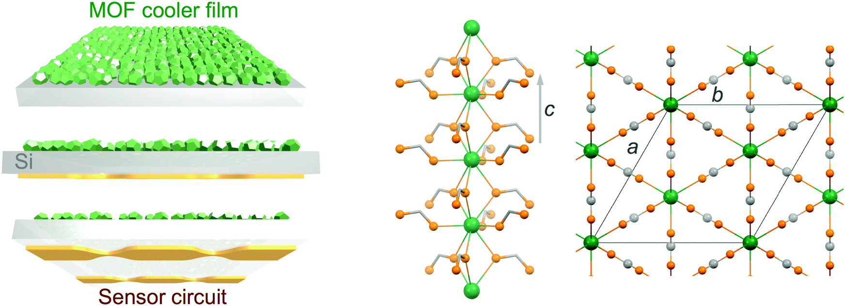 | ||
| Scheme 1 Left: Schematic representation of an integrated device, in which a superficial layer of molecular-based cooler particles would allow local micro-refrigeration of a silicon membrane and a sensor circuit built on its surface. Right: Views of the structure of the gadolinium formate MOF Gd(HCOO)3, selected here for its high magneto-caloric effect. Colour code: Gd, green spheres; O, orange spheres; C, grey spheres or sticks. | ||
2. Experimental
2.1 Material synthesis
All reagents were purchased from Aldrich and used as received. HF (48% in water), ethylacetate (>99%, GC), 1,2-dimethoxyethane (>99%, reagent grade) and acetone (>99.5%, reagent grade) were purchased from Aldrich, while CH2Cl2 (99.8% + 50 ppm amylene, synthesis grade) and absolute EtOH (99.9%, synthesis grade) were obtained from Scharlab. The water used in all manipulations was Milli-Q water (resistivity >18 MΩ cm). Si(100) and Si(111) wafers were purchased from Si-Mat. Au-covered Si substrates were obtained by evaporating 10 nm of Cr, to improve adhesion, and 100 nm of Au onto a 4 inch Si(100) wafer. Pieces of variable sizes in the range 0.25–2 cm2 were cut out of the different types of substrates.The dried substrates were immediately transferred to a round-bottom flask under Ar containing the alkene, either 1-undecene (97%) or 10-undecenoic acid (98%), in sufficient amount to cover the H–Si(111) substrates. Under a continuous Ar flow, the temperature was then increased to 175 °C in about 20 min and kept for 4 h at 178–182 °C. After cooling to ca. 50 °C, the alkene was removed and the substrates were washed twice with ethylacetate and twice with CH2Cl2 to remove the excess unreacted alkene. After a final washing with acetone, the substrates were dried under a flow of N2 and used right away.
2.2 Physical characterization
3. Results and discussion
3.1 Pre-functionalization by monolayer formation and characterization
Because basically no studies of MOF growth on oxide-free Si are available and the optimal growth conditions for a specific MOF are difficult to predict, several approaches have been used here for the formation of carboxylic acid monolayers on oxide-free Si. A first approach involves the formation of SAMs on the bare Si(100) surface with mercapto-undecanoic acid (MUDA) and mercapto-hexadecanoic acid (MHDA) in ethanol, the resulting samples being hereafter denoted 1(C11) and 1(C16). For comparison, the same MUDA SAM was formed on a gold layer grown on Si(100), denoted 1Au(C11). A second strategy uses the thermally-induced hydrosilylation of a hydrogen-terminated Si surface16 using neat undecenoic acid, the resulting sample being denoted 2. The Si(111) surface is preferred in this case due to the ability to form a higher density of Si–H bonds. A third strategy involves the light-activated hydrosilylation of H–Si(111)17 with neat undecynoic acid, the resulting sample being denoted 3. The same conditions were used to form samples with similar albeit hydrophobic SAMs, i.e., using undecanethiol (denoted 1(C11)ref and 1Au(C11)ref), undecene (2ref) and dodecyne (3ref), for comparison with the literature. These approaches and the corresponding abbreviations used are summarized in Table 1.| Code | Substrate | Method/reagenta | θ s (°) | Atomic ratio C/Si | Roughness (nm) |
|---|---|---|---|---|---|
| a UDT = 1-undecanethiol, MUDA = 11-mercapto-undecanoic acid and HMDA = 16-mercapto-hexadecanoic acid. b Thiol-based self-assembled monolayers. c Thermally-induced. d Light-activated. | |||||
| 1(C11)ref | Si(100) | SAMb/UDT | 89 | 15.5/84.5 | 0.24 |
| 1(C11) | Si(100) | SAMb/MUDA | 70 | 19.1/80.9 | 2.4 |
| 1(C16) | Si(100) | SAMb/HMDA | 68 | 21.2/78.8 | 1.4 |
| 1Au(C11)ref | Au@Si | SAMb/UDT | 90 | N/A | — |
| 1Au(C11) | Au@Si | SAMb/MUDA | 40 | N/A | 0.2 |
| 2ref | Si(111) | Hydrosilylationc/undecene | 96 | 36.8/63.2 | 1.3 |
| 2 | Si(111) | Hydrosilylationc/undecenoic acid | 45 | 33.2/66.8 | 0.75 |
| 3ref | Si(111) | Hydrosilylationd/dodecyne | 98 | 36.9/63.1 | — |
| 3 | Si(111) | Hydrosilylationd/undecynoic acid | 42 | 32.8/67.2 | 0.35 |
Static contact angles θs were measured for all the monolayers with Milli-Q water drops (Fig. S2 and S3, ESI†), and are presented in Table 1. As expected, the monolayers made with alkyl end groups have θs characteristics of hydrophobic surfaces, while those for carboxylic end groups are indicative of hydrophilic surfaces. In particular, the θs of the hydrophobic monolayers obtained by hydrosilylation, 96° for 2ref and 98° for 3ref, are comparable with those previously reported using an hexadecyl chain.18 The corresponding monolayers with carboxylic acid end groups 2 and 3 have similar θs, also comparable with that for 1Au(C11), in the range 40°–45°, indicating carboxylic acid monolayers of high quality and surface coverage. In contrast, the larger θs of 70° and 68° for 1(C11) and 1(C16), respectively, are a clear indication of incomplete disordered monolayers. Considering a reported correlation of surface density for binary homogeneous SAMs of undecanethiol and MUDA on Au,19 these values would correspond to a surface with only ca. 50% coverage by MUDA. Using the same correlation, θs of 1Au(C11), 2 and 3 would correspond to a relative surface coverage >90%.20
The monolayers were analysed by XPS, and the characteristic survey and narrow scans are given in Fig. S4–S9 (ESI†). Except for the Au-coated substrates where this is irrelevant, the absence of any significant amounts of silicon dioxide is confirmed by the flat baseline in the range 103–104 eV. Meanwhile, the presence of thiol molecules is confirmed by the detection of S 2p peaks. Deconvolution of the C 1s narrow scans shows the expected signal of the oxidized carbons at ca. 288.5 eV for the carboxylic acid-terminated monolayers, in addition to the main peak of the aliphatic carbons at 284.9 eV and adventitious contaminations at ca. 286 eV. For the hydrosilylated monolayers, the silicon-bound carbons are also discernible at ca. 283.2–283.7 eV, and the relative ratios with the aliphatic carbons are close to those expected. Besides this chemical characterization, the analysis of the XPS data also evidences the differences in quality of the monolayers indicated by the contact angles, through much lower atomic C/Si ratios in the case of thiol SAMs with respect to the covalent monolayers obtained by hydrosilylation.
In fact, the atomic C/Si ratio can be used to estimate the monolayer density and height.21,22 Here, the C/Si ratios for 2ref and 3ref are ca. 0.58, similar to previously reported values for dense monolayers with a thickness of ca. 18 Å.23 The corresponding analysis done for the carboxylic acid-terminated monolayers 2 and 3 gave a slightly smaller value of ca. 0.49, which would correspond to a monolayer thickness of ca. 16 Å, still pointing to well-ordered and dense monolayers. Comparatively, 1(C11) and 1(C16) have C/Si ratios about 2.5 times smaller, i.e., the monolayers are about 8–10 Å thin, confirming a very incomplete and disordered surface coverage. AFM topographic images of 1(C11), 1(C16) and 1Au(C11) reveal that indeed the former two are less uniform, as indicated by their average roughness of 2.4 and 1.4 nm, to be compared with a roughness of 0.6 nm for the latter, similar to the clean Au surface (Fig. S16–S18, ESI†). The lower roughness in the case of 1(C16) is likely due to a relatively better order promoted by longer alkyl chains. The topography of all hydrosilylated monolayers is homogeneous with a roughness in the range 0.35–0.75 nm, associated with the domains formed through this strategy.24 Interestingly, the height of the monolayer derived by mechanically scratching it from the Si(111) substrate is ca. 2.0 nm, in good agreement with the estimation done on the basis of the C/Si from XPS data.
Overall, monolayers with carboxylic acid end groups of various qualities have been grown on oxide-free Si. The thiol-based SAMs have a poor surface coverage and are likely disordered. While this can reasonably be associated with the much weaker Si–S interaction compared with the Au–S one, this does not necessarily impede the growth of the selected Gd(HCOO)3 MOF. In contrast, the monolayers obtained by hydrosilylation are dense and highly-ordered, and possess a further advantage in their high chemical and thermal stability,25 due to the formation of covalent Si–C bonds. Alkynes normally form better (denser) monolayers than alkenes,23 but the relatively small difference may actually have no effect on the MOF growth.
3.2 Growth and characterization of gadolinium formate
The same growth procedure was used for all freshly prepared carboxylic acid-terminated monolayers, involving immersion for 24 h of the Si substrate in an ethanol solution of Gd(HCOO)3 close to saturation. The morphology of the formed material was analyzed using FESEM (Fig. 1 and Fig. S11–S15, ESI†) and AFM (Fig. 2) measurements, revealing significant differences correlated with the quality of the subjacent monolayer.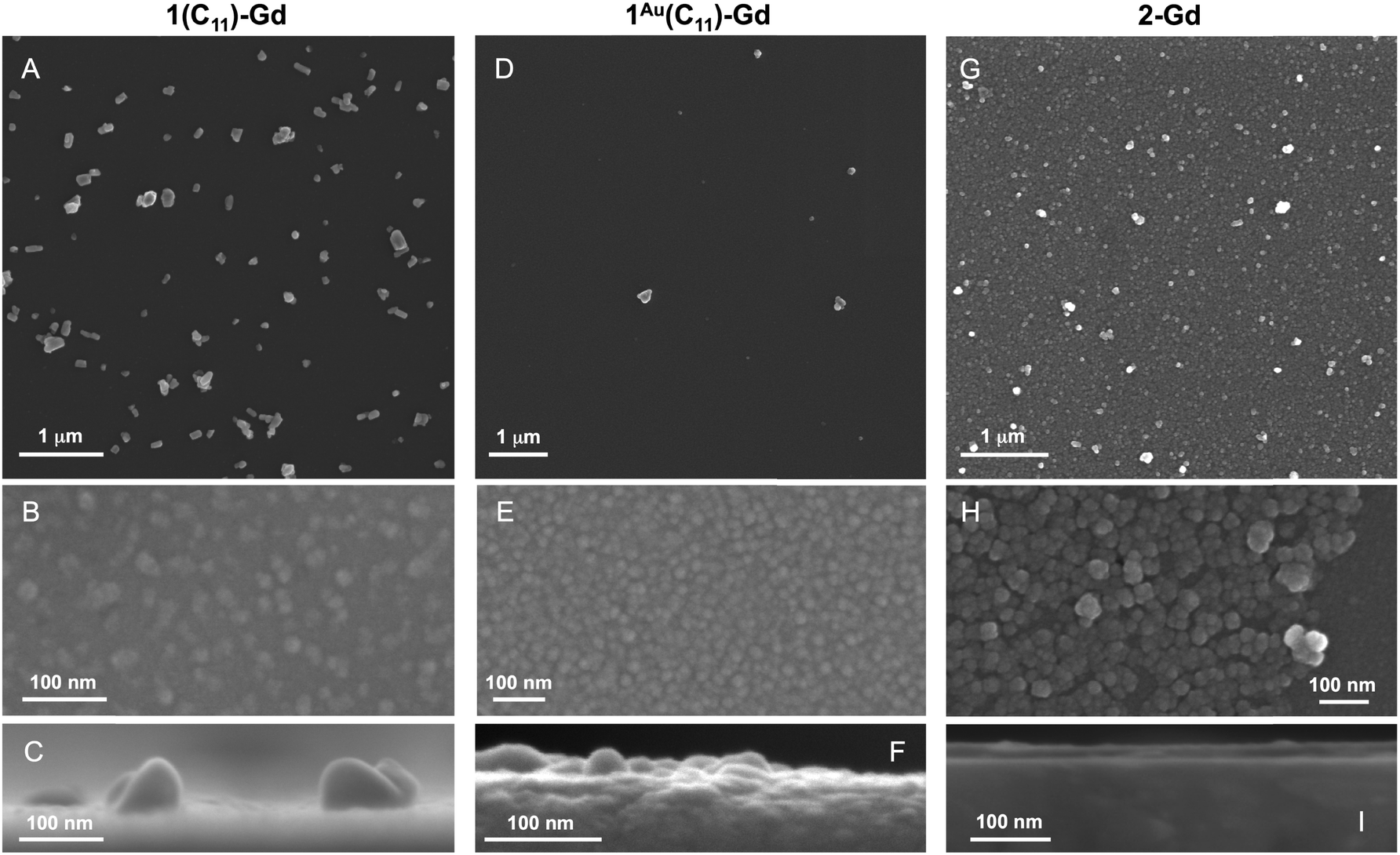 | ||
| Fig. 1 Characteristic FESEM images of the Gd(HCOO)3 MOF grown on thiol-based SAM on oxide-free Si(100) (1(C11)-Gd, left) and a Au layer grown on oxide-free Si(100) (1Au(C11)-Gd, center), and the covalent monolayer obtained by hydrosilylation of Si(111) (2-Gd, right). Images C, F and I are cross-section views. | ||
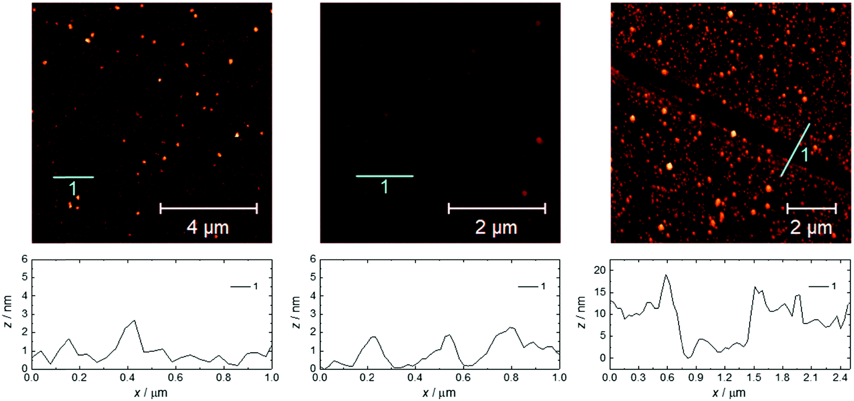 | ||
| Fig. 2 AFM topography images and the relative surface profiles for 1(C11)-Gd (left), 1Au(C11)-Gd (center) and 2-Gd (right). The respective RMS surface roughnesses are 1.3, 0.5 and 4.3 nm. | ||
For the thin films grown on thiol-based SAMs 1(C11)-Gd and 1(C16)-Gd, two different forms of grown material are present. Large nanocrystals with height of the order of 50–100 nm and length from 100 to 500 nm have formed but only cover a limited fraction of the whole surface (Fig. 1A and C, and Fig. S11A and C, ESI†), the remainder being covered by small to very small clusters, all this pointing to a 3D growth (Fig. 1B and Fig. S11B, ESI†). Full coverage of the substrate surface is unclear from the FESEM images. The root mean square (RMS) surface roughness is 5.3 nm for 1(C11)-Gd and 2.1 nm for 1(C16)-Gd, significantly higher than the bare SAMs and therefore pointing at a thin layer of grown material. This is also confirmed by the absence of these smaller objects when subjecting the hydrophobic 1(C11)ref SAM to the same growth conditions (Fig. S12, ESI†). The surface of 1Au(C11)-Gd almost only exhibits a similar thin layer of clusters, albeit more continuous and apparently thicker, plus only very few larger nanocrystals (Fig. 1D and E). Eventually, the topography of 2-Gd and 3-Gd depicts a homogeneous complete coverage of the substrate by larger clusters of sizes in the range 15–40 nm, and the absence of large nanocrystals (Fig. 1G–I and Fig. S13, ESI†). The rather homogenous size of the grown crystallites and complete coverage result in a still limited roughness of 0.5 nm. The thickness of the grown film as evaluated through mechanical scratches remains limited though at ca. 10 nm. Nonetheless, the amount of the grown material can be increased by extending the immersion time of the functionalized substrate in the Gd(HCOO)3 solution (see below). EDS indicates the presence of Gd in the larger nano-crystals, but not in the cluster thin layers of 1(C11)-Gd, 1(C16)-Gd and 1Au(C11)-Gd. This is however likely due to the limitations of EDS to detect elements in the most superficial part of a specimen. Anyhow, XPS confirms the presence of Gd in all thin films through the clear detection of the Gd 3d5/2 emission at 1185 eV (Fig. S10, ESI†). In addition, deconvolution of the C 1s peaks indicates a significant relative increase of carboxylic acid C, which can reasonably be associated with formate groups from Gd(HCOO)3. Therefore, the chemical composition of the grown crystallites agrees with the hypothesis that these are all the same Gd(HCOO)3 material. Eventually, X-ray diffraction confirms the identity of the material grown on both thiol and hydrosilylated monolayers (Fig. 3). The patterns match those calculated from the single-crystal structure of Gd(HCOO)3, demonstrating the successful growth of the selected MOF cooler on Si without impurity phases. Although the formed thin films are polycrystalline, the patterns indicate a significant preferential orientation along (110). An exception is 1Au(C11)-Gd, for which the only (weak) diffraction peak corresponds to the (211) plane, pointing at a different growth mechanism for the continuous thin layer. This means that the diffraction patterns of 1(C11)-Gd and 1(C16)-Gd are likely associated with the larger crystallites, in agreement with the relatively strong diffraction detected using a standard diffractometer. Obtaining diffraction patterns for 2-Gd required grazing-incidence X-ray diffraction, likely due to the smaller size of the crystallites. The (110) preferred orientation observed for both 1(C11)-Gd and 2-Gd is one of the Gd-rich planes in the structure of Gd(HCOO)3 (Scheme 1), therefore corresponding to an optimal situation to initiate the growth through coordination of Gd(III) ions from the solution by the monolayer carboxylic end groups (Fig. 4).
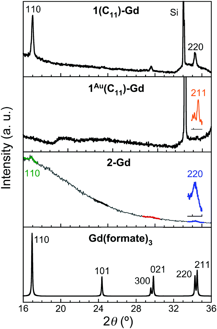 | ||
| Fig. 3 X-ray diffraction patterns for 1(C11)-Gd, 1Au(C11)-Gd and 2-Gd, compared with the calculated patterns obtained from the single-crystal structure of Gd(HCOO)3, as indicated. The practical absence of the (101), (300) and (021) peaks in the patterns of 1(C11)-Gd and 2-Gd point at a preferential orientation along (110). | ||
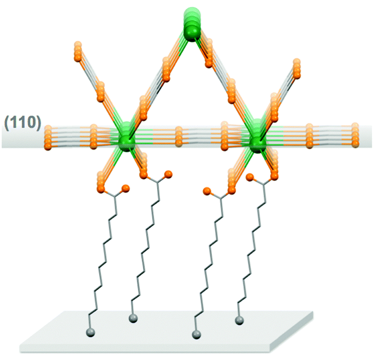 | ||
| Fig. 4 Representation of the main preferred Gd(HCOO)3 growth direction on the carboxylate-terminated monolayers. The coordination anchoring mode is hypothetical. Colour code: Gd, green spheres; O, orange spheres; C, grey sticks. The grey spheres represent the connection to the silicon, either through a S–Si interaction or a C–Si covalent bond. | ||
Overall, Gd(HCOO)3 crystallites do grow on carboxylic acid monolayers on oxide-free Si, although their size, morphology, and most importantly the growth efficiency clearly depend on the quality and type of the underlying monolayer. Even for the more favorable covalent monolayers obtained by hydrosilylation, the observed surface-growth of Gd(HCOO)3 is clearly less efficient than previously reported for a number of porous MOFs.14 These were however obtained by the so-called liquid-phase epitaxy method,14,26 in which the substrate is exposed sequentially to the different components of the MOF, i.e., metal ions and linkers. We had originally attempted a similar method, using GdCl3 and ammonium formate solutions, but this proved unsuccessful. The sequential growth method is in principle optimal for MOFs with pillared layered structures, which could explain its inefficiency here with Gd(HCOO)3, although dense coatings have been successfully formed by this method with a few other 3D unpillared MOFs.27 Another limitation is the solubility of Gd(HCOO)3 that does not allow an increase in the concentration of the immersion solution, already close to saturation. Here, nevertheless, the probable most relevant parameter for the MOF growth is the metal ion itself and the associated lability and reactivity. Indeed, most carboxylate-based MOFs grown so far through sequential methods have been Cu(II) MOFs,14,26 many based on paddle-wheel Cu2(RCOO)4 nodes, and therefore quite different from the connectivity in the structure of Gd(HCOO)3. Rapid ligand exchange kinetics typically occurring at Cu(II) ions are key for an efficient sequential layer-by-layer growth. Gd(III) is comparatively a kinetically inert ion and this could explain a comparatively poor on-surface growth.
Besides the simple 24 h immersion, we have also tested multiple shorter immersions, which lead to no significant modifications in terms of quality, homogeneity and quantity of the grown material. In particular, repeated short immersions of 1(C11) do not impede the growth of large crystallites. These are also formed when using a 10-fold diluted Gd(HCOO)3 solution (Fig. S14, ESI†). Altogether, this would indicate that the formation of these large crystallites is associated with the comparatively poor quality of the thiolated SAM, which likely results in preferential nucleation and growth at either defects or, more likely, well-ordered areas.
Longer immersions of 48 h were also performed on 2, both refreshing the Gd(HCOO)3 solution after 24 h or using the same solution for the whole 48 h (2-Gd48h). The FESEM observations (Fig. S15, ESI†) together with the estimation of the amount of material grown through magnetic measurements (see next section) indicate that the amount of surface-grown Gd(HCOO)3 can be increased through the immersion time. Such ability to adjust the amount of grown material is particularly important for the proper cooling of the substrate, as discussed in the next section. The only disadvantage could be a comparatively less homogeneous thin film, as indicated by the observation for 2-Gd48h of some larger crystallites on top of a continuous film similar to that observed for 2-Gd.
3.3 Magnetic properties and refrigeration potential
The magnetization of the made thin films was found sufficient to be detected at low temperatures by standard RSO-SQUID magnetometry (∼10−8–10−9 emu), thus allowing a measure of the amount of Gd(HCOO)3 grown on each type of substrate (see the ESI,† Fig. S19–S21). The temperature dependence of the magnetic susceptibility in the 2–50 K range and isothermal magnetization at 2 and 5 K were determined for the Gd(HCOO)3 grown films in 1(C11)-Gd, 1(C16)-Gd, 1Au(C11)-Gd, 2-Gd, 3-Gd and 2-Gd48h (Fig. 5 and Fig. S22, ESI†). For this, the diamagnetic contributions of the bare 100 and 111 Si wafers were experimentally determined under the same isofield and isothermal conditions and subtracted to the corresponding total magnetization, thus providing the raw magnetic response of the grown materials (Fig. S19, ESI†).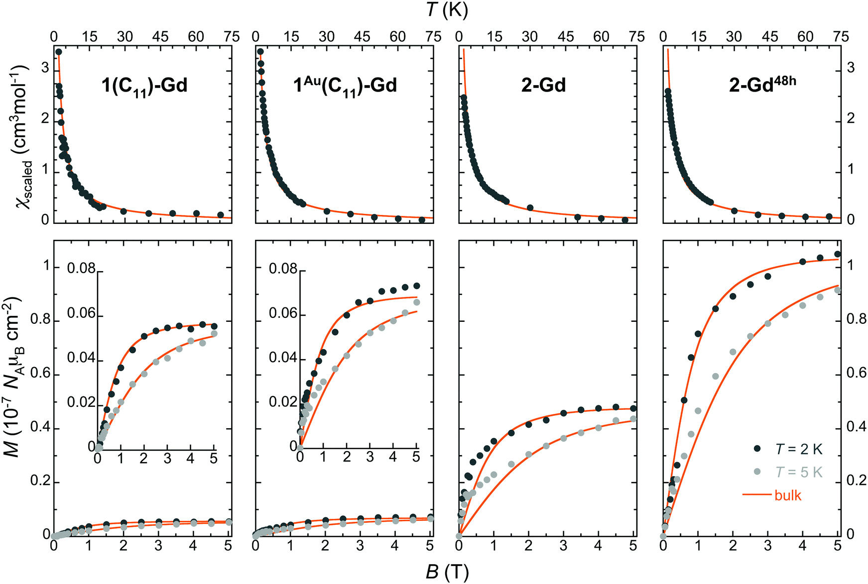 | ||
| Fig. 5 Magnetic properties of the Gd(HCOO)3 thin films grown on oxide-free silicon with different subjacent carboxylic monolayers, as indicated. Top: Temperature dependence of the molar magnetic susceptibility obtained by scaling to the bulk material data shown as thick lines. Bottom: Isothermal field dependence of the molar magnetization per surface area at 2 and 5 K, as determined by comparison with the bulk material data (see the ESI† for details). The data are shown using the same range to evidence the significant differences arising from the subjacent carboxylate monolayers and growth time. For 1(C11)-Gd and 1Au(C11)-Gd, the data are also shown with a more adequate range as insets. The scaled bulk material data are shown as thick lines. | ||
Given that the amount of deposited material is initially unknown, these data, obtained in emu units, are then scaled to the molar magnetization and susceptibilities of the bulk Gd(HCOO)3 parent material (solid lines in Fig. 5 and Fig. S20, ESI†). For all the samples, the agreement is good for both magnetization and susceptibility experiments, thus demonstrating that the magnetic properties of Gd(HCOO)3, and so its corresponding MCE, are maintained in the surface-grown nano-crystals. It is noteworthy that the same factor used to scale the M vs. B data collected for 2 and 5 K can also be employed for scaling satisfactorily the M vs. T data for each sample. As the scaling procedure involves separate experiments, this ensures the reliability of the results and, indirectly, an estimate of the mass of the grown materials. The obtained Gd(HCOO)3 surface densities indicate significant differences between the growth on thiol-based SAMs and hydrosylilated covalent monolayers, in line with the semi-quantitative Gd/C ratios determined by XPS (Table 2). Indeed, while the growth conditions and time are identical, 2-Gd and 3-Gd have Gd(HCOO)3 surface densities about one order of magnitude larger than those of 1(C11)-Gd, 1(C16)-Gd and 1Au(C11)-Gd. Similar surface densities for the latter three can be reasoned in light of the presence or absence of large crystals. Indeed, while the better quality of the subjacent SAM for 1Au(C11)-Gd gives rise to a more homogeneous layer than for 1(C11)-Gd and 1(C16)-Gd, this is likely compensated by the volume of the larger crystals present only in the latter two samples. Then, the 10-fold increase of surface density between 1Au(C11)-Gd and 2-Gd and 3-Gd, all with dense ordered subjacent carboxylic acid monolayers, necessarily means that not only its quality, but also its type, i.e., physisorbed vs. covalent, is relevant to the MOF growth, as already indicated by FESEM observations. Here, it is significant that the growth occurs in EtOH, the same solvent used to elaborate the thiol-based SAMs. The dynamic processes occurring for thiol-based SAMs in contact with their solution are therefore active, and may represent a limitation for a MOF growth involving coordination bond formation with kinetically inert Gd(III) ions.
| Sample | Roughness | Atomic ratio Gd/Si | Surface density [10−7 g cm−2] |
|---|---|---|---|
| a For 2-Gd48h, a few bunches of large crystallites are present on top of the main deposit. The roughness given is for areas without such larger crystallites and therefore describing the grown material. The roughness of large areas (e.g., 10 μm × 10 μm or larger) containing some larger crystallites is >21. | |||
| 1(C11)-Gd | 5.3 | 0.00035 | 2.4 |
| 1(C16)-Gd | 2.1 | 0.00041 | 2.9 |
| 1Au(C11)-Gd | 0.75 | N/A | 2.9 |
| 2-Gd | 4.7 | 0.00067 | 20.2 |
| 2-Gd48h | 2.75a | — | 43.8 |
| 3-Gd | 0.4 | 0.00131 | 28.6 |
Next, we evaluate the cooling potential of our Gd(HCOO)3 thin films. In an on-chip microrefrigerator, the magnetocaloric material would be deposited on a silicon substrate,12 manufactured in the form of a suspended membrane (see Scheme 1). Heat transfer has to proceed via low-energy phonons, because of the low working temperatures. The anchor molecules with a carboxylic end function should not hinder the conduction of heat between the Gd(HCOO)3 crystallites and the silicon substrate. The soft, flexible nature of the aliphatic chains of the anchor molecules provides numerous degrees of freedom and, therefore, they should couple well with low-temperature vibrational modes.
We tentatively assume that the membrane has a thickness of 2 μm and that its low-temperature heat capacity is significantly larger than that of any other component of the device but the Gd(HCOO)3 thin film. We also assume ideal experimental conditions, that is, the refrigeration by demagnetization proceeds adiabatically. For the sake of exemplification, let us focus on the representative 1(C11)-Gd and 3-Gd solely, and on the starting conditions of the adiabatic demagnetization that can be easily accessed by cryocoolers and permanent magnets, e.g., T = 5 K and B = 2 T, respectively. Fig. 6 shows the temperature dependencies of the entropies for 1(C11)-Gd and 3-Gd alone (dotted lines), together with the entropies of the system (solid lines) that comprises either 1(C11)-Gd or 3-Gd and the Si membrane of 2 μm thickness (Si2μm), thermally linked to the corresponding MOF material. The contributions of 1(C11)-Gd and 3-Gd are obtained from the experimentally determined entropy of the parental Gd(HCOO)3 bulk material,8a properly rescaled by the corresponding surface densities (Table 2). The contribution of Si2μm is calculated from the Debye temperature of 645 K, as for silicon, which is then added to the entropies of 1(C11)-Gd and 3-Gd, respectively (Fig. 6). The lowest temperature that can be attained by the proposed adiabatic demagnetization (blue arrows in Fig. 6) is markedly different, depending on the representative film considered. Specifically, 3-Gd permits reaching ca. 0.8 K after a full demagnetization down to zero applied field, whilst only ca. 3.3 K can be attained with 1(C11)-Gd under the same conditions, making the latter magnetocaloric thin film barely useful for the proposed target. The reason for such a difference is nothing but the relative amount of magnetocaloric material present, viz., the higher its surface density, the relatively lower the contribution of Si2μm and, therefore, the resulting temperature change is closer to the bulk behavior. Interestingly, the surface density of the grown Gd(HCOO)3 is found to double when the growth time of hydrosylilated covalent monolayers is increased from 24 to 48 h. This clearly demonstrates that thicker films of Gd(HCOO)3 can be grown, to provide the necessary and sufficiently large refrigeration capacity. Therefore the Si membranes, that are now developed and used for a number of applications,28 would be efficiently cooled by our still un-optimized gadolinium formate thin layers.
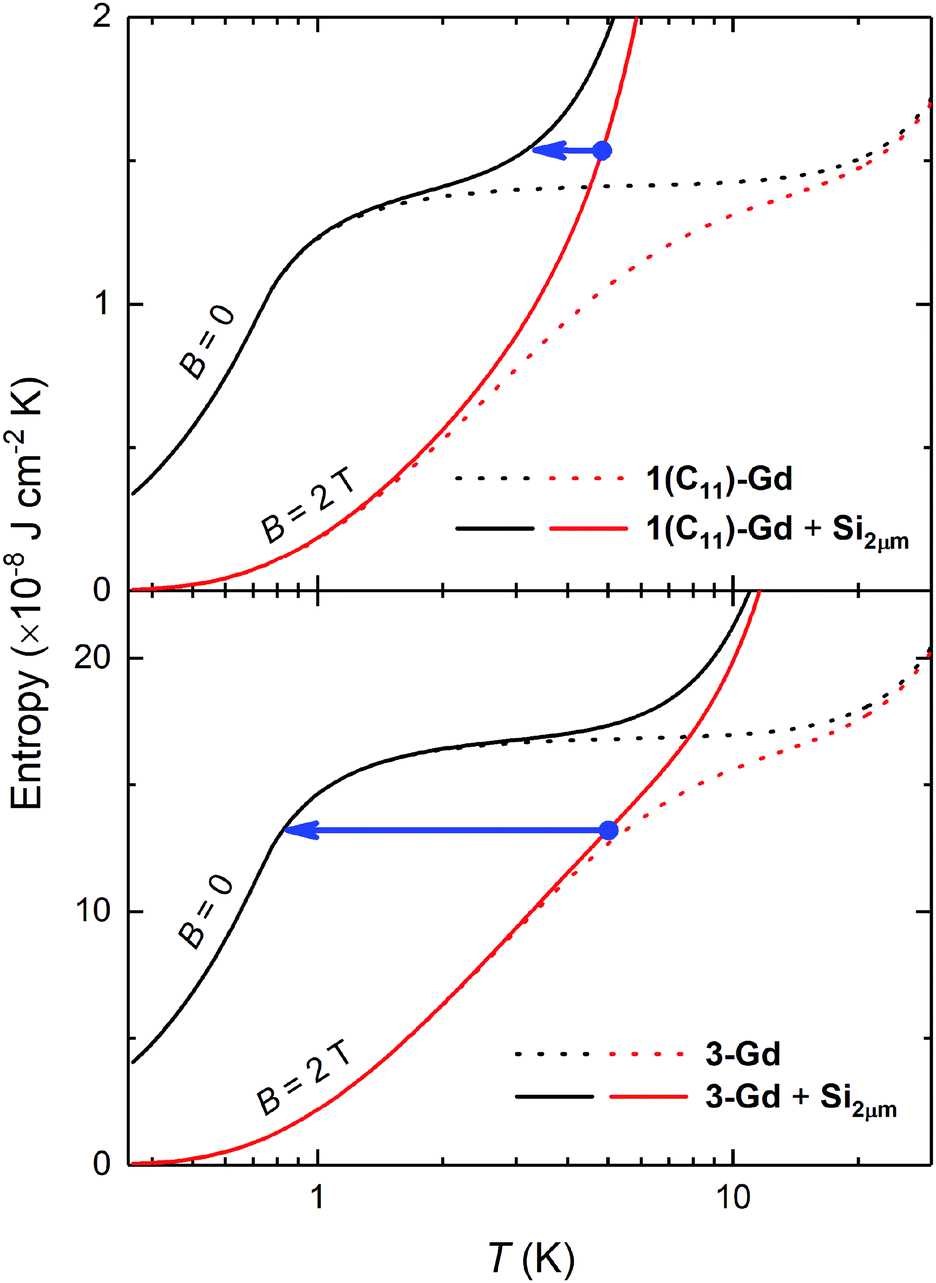 | ||
| Fig. 6 Temperature dependence of the entropy for B = 0 and 2 T, normalized to the surface area of the substrate, for 1(C11)-Gd (top) and 3-Gd (bottom), with (solid lines) and without (dotted lines) the contribution of a thermally-contacted Si membrane of 2 μm thickness (Si2μm), as indicated. The blue arrow indicates an adiabatic demagnetization of the MOF material that, starting from T = 5 K and B = 2 T, decreases its temperature and that of Si2μm down to 0.8 K for 3-Gd and, only, to 3.3 K for 1(C11)-Gd, when reaching zero applied field. | ||
4. Conclusions
The gadolinium formate MOF can be grown on oxide-free Si covered with carboxylate-terminated monolayers by immersion in a concentrated solution of the bulk material at ambient temperature. This provides a functionalized surface with a local source of magnetic refrigeration for temperatures below 10 K, through the large magneto-caloric effect of gadolinium formate. The quality and type of the carboxylate-terminated monolayer is, however, critical for the growth efficiency and therefore the amount of grown MOF and its associated cooling power. Covalent monolayers obtained by thermal or photo-induced hydrosilylation of Si(111)–H surfaces give the best result, likely due to their high quality and full surface coverage, as well as their robustness compared to physisorbed SAMs. The hydrosilylation strategy also has the advantage of being applicable to oxide-free Si3N4,29 the other material with a low-temperature small heat capacity and used as a device support. Importantly, the amount of grown MOF can be increased according to the immersion time. The still rather thin MOF layers reported here already provide an estimated relative cooling potential per surface area sufficient to efficiently cool the Si or Si3N4 membranes currently developed for a number of applications. This work is the first exploration of the growth of a Gd(III) MOF on oxide-free Si, and improvements may be expected from considering other carboxylate-based MOFs, for which the method used here should be extendable. Increasing the growth temperature may also be useful to improve the quality and thickness of the Gd(III) MOF layers, as it is already known to strongly influence on-surface growth of MOFs with Cu(II),30 a highly labile metal ion compared to Gd(III). Altogether, our results show that local on-chip magnetic refrigeration at cryogenic temperatures may be provided by thin layers of molecular-based coolers, and we are currently working on directly measuring their cooling efficiency.Conflicts of interest
There are no conflicts of interest to declare.Acknowledgements
The authors acknowledge funding from the Spanish MINECO and FEDER through projects MAT2014-53961-R (GL, EN and OR), MAT2015-70868-ERC (OR), MAT2015-68204-R (GL and ME) and MAT2017-86826-R (OR and EN), as well as from the Aragón government (DGA, consolidated groups MOLCHIP E98, PLATON E31_17R and M4 E13_17R). The authors are grateful to Dr G. Antorrena (LMA) for his help with XPS and GIXRD experiments, to Dr J. Sesé for providing the Si wafers and to Dr J. Stankiewicz for her help with Au deposition.References
- (a) M. N. Leuenberger and D. Loss, Nature, 2001, 410, 789 CrossRef CAS PubMed; (b) Molecular Magnets: Physics and Applications, ed. J. Bartolomé, F. Luis and J. F. Fernández, Springer, 2014 Search PubMed.
- (a) A. Ardavan, O. Rival, J. Morton, S. Blundell, A. Tyryshkin, G. Timco and R. E. P. Winpenny, Phys. Rev. Lett., 2007, 98, 057201 CrossRef PubMed; (b) G. Aromí, D. Aguilà, P. Gamez, F. Luis and O. Roubeau, Chem. Soc. Rev., 2012, 41, 537 RSC.
- (a) M. Evangelisti and E. K. Brechin, Dalton Trans., 2010, 39, 4672 RSC; (b) R. Sessoli, Angew. Chem., Int. Ed., 2012, 51, 43 CrossRef CAS PubMed.
- (a) W. F. Giauque, J. Am. Chem. Soc., 1927, 49, 1864 CrossRef CAS; (b) R. P. Hudson, Principles and Applications of Magnetic Cooling, North-Holland, Amsterdam, 1972 Search PubMed; (c) V. K. Pecharsky and K. A. Gschneider, J. Magn. Magn. Mater., 1999, 25, 44 CrossRef.
- (a) A. M. Tishin and Y. I. Spichkin, The magnetocaloric effect and its applications, Series in Condensed Matter Physics, IOP, Bristol, 2003 CrossRef; (b) V. Franco, J. S. Blázquez, J. J. Ipus, J. Y. Law, L. M. Moreno-Ramírez and A. Conde, Prog. Mater. Sci., 2018, 93, 112 CrossRef.
- (a) A. T. Serlemitsos, B. A. Warner, S. Castles and S. R. Breon, Adv. Cryog., 1990, 35B, 1431 Search PubMed; (b) P. J. Shirron, Cryogenics, 2014, 62, 130 CrossRef CAS.
- Examples of molecular coolers with high volumetric MCE: (a) M. Evangelisti, O. Roubeau, E. Palacios, A. Camón, T. N. Hooper, E. K. Brechin and J. J. Alonso, Angew. Chem., Int. Ed., 2011, 50, 6606 CrossRef CAS PubMed; (b) L.-X. Chang, G. Xiong, L. Wang, P. Cheng and B. Zhao, Chem. Commun., 2013, 49, 1055 RSC; (c) F.-S. Guo, Y.-C. Chen, L.-L. Mao, W.-Q. Li, J.-D. Leng, R. Tarasenko, M. Orendác, J. Prokleska, V. Schovsky and M.-L. Tong, Chem. – Eur. J., 2013, 19, 14876 CrossRef CAS PubMed.
- Examples of Metal–Organic Frameworks with high volumetric MCE: (a) G. Lorusso, J. W. Sharples, E. Palacios, O. Roubeau, E. K. Brechin, R. Sessoli, A. Rossin, F. Tuna, E. J. L. McInnes, D. Collison and M. Evangelisti, Adv. Mater., 2013, 25, 4653 CrossRef CAS PubMed; (b) R. Sibille, T. Mazet, B. Malaman and M. François, Chem. – Eur. J., 2012, 18, 12970 CrossRef CAS PubMed; (c) G. Lorusso, M. A. Palacios, G. S. Nichol, E. K. Brechin, O. Roubeau and M. Evangelisti, Chem. Commun., 2012, 48, 7592 RSC; (d) Y.-C. Chen, L. Qin, Z.-S. Meng, D.-F. Yang, C. Wu, Z. Fu, Y.-Z. Zheng, J.-L. Liu, R. Tarasenko, M. Orendác, J. Prokleska, V. Sechosky and M.-L. Tong, J. Mater. Chem. A, 2014, 2, 9851 RSC; (e) C. Das, A. Upadhyay, K. Uddin Ansari, N. Ogiwara, T. Kitao, S. Horike and M. Shanmugam, Inorg. Chem., 2018, 57, 6584 CrossRef CAS PubMed.
- (a) J. W. Sharples and D. Collison, Polyhedron, 2013, 54, 91 CrossRef CAS; (b) M. Evangelisti, Molecule-based magnetic coolers: measurement, design and application, in Molecular Magnets. Physics and Applications, ed. F. Luis, J. Bartolomé and J. F. Fernandez, Springer-Verlag, Berlin, Heidelberg, 2014, pp. 365–387 Search PubMed.
- O. Roubeau, E. Natividad, M. Evangelisti, G. Lorusso and E. Palacios, Mater. Horiz., 2017, 4, 464 RSC.
- V. Corradini, A. Ghirri, A. Candini, R. Biagi, U. del Pennino, G. Dotti, E. Otero, F. Choueikani, R. J. Blagg, E. J. L. McInnes and M. Affronte, Adv. Mater., 2013, 25, 2816 CrossRef CAS PubMed.
- G. Lorusso, M. Jenkins, P. Gónzalez-Monje, A. Arauzo, J. Sesé, D. Ruiz-Molina, O. Roubeau and M. Evangelisti, Adv. Mater., 2013, 25, 2984 CrossRef CAS PubMed.
- Electronic schemes currently exploited produce only limited ΔT of the order of 0.1 K, see J. T. Muhonen, M. Meschke and J. P. Pekola, Rep. Prog. Phys., 2012, 75, 046501 CrossRef PubMed.
- (a) A. Bétard and R. A. Fischer, Chem. Rev., 2012, 112, 1055 CrossRef PubMed; (b) J. Liu and C. Wöll, Chem. Soc. Rev., 2017, 46, 5730 RSC.
- This has been assessed due its importance in Si-based electronics, see: (a) O. W. Käding, H. Skurk and K. E. Goodson, Appl. Phys. Lett., 1994, 65, 1621 CrossRef; (b) L. J. McDaid, S. Hall, P. H. Mellor, W. Eccleston and J. C. Alderman, Electron. Lett., 1989, 25, 827 CrossRef.
- (a) M. R. Linford, P. Fenter, P. M. Eisenberger and C. E. D. Chidsey, J. Am. Chem. Soc., 1995, 117, 3145 CrossRef CAS; (b) A. B. Sieval, A. L. Demirel, J. W. M. Nissink, M. R. Linford, J. H. Van der Maas, W. H. De Jeu, H. Zuilhof and E. J. R. Sudhölter, Langmuir, 1998, 14, 1759 CrossRef CAS; (c) P. Thissen, O. Seitz and Y. J. Chabal, Prog. Surf. Sci., 2012, 87, 272 CrossRef CAS.
- L. Scheres, A. Arafat and H. Zuilhof, Langmuir, 2007, 23, 8343 CrossRef CAS PubMed.
- Reported values under optimized conditions are respectively 100° and 108°. The larger difference obtained here with dodecyne can be ascribed to the shorter alkyl chain, as this has been shown to affect the surface coverage when using alkynes while having no effect when using alkenes, see ref. 23.
- S.-I. Imabayashi, N. Gon, T. Sasaki, D. Hobara and T. Takiuchi, Langmuir, 1998, 14, 2348 CrossRef CAS.
- Note that for the hydrosilylated substrates, this is not corresponding to the true surface coverage, i.e. the fraction of surface atoms that have formed a Si–C bond. It has been shown that surface coverages of up to 55 and 65% can be reached respectively with alkenes and alkynes, see ref. 23.
- X. Wallart, C. Henry de Villeneuve and P. Allongue, J. Am. Chem. Soc., 2005, 127, 7871 CrossRef CAS PubMed.
- Using the relation dML (Å) = λSiML
![[thin space (1/6-em)]](https://www.rsc.org/images/entities/char_2009.gif) sin(φ)ln(1 + C/Si), where λSiML is the attenuation length of Si2p photoelectrons in the organic monolayer and φ is the angle between the surface plane and the detector, taken as 90°; see ref. 21. The derived thicknesses should however be taken only as rough estimations because the C/Si ratios obtained here are not truly quantitative. This is because the influence of photodiffraction on the XPS signal is not taken into account as done in ref. 21 by rotating the samples by 360° around the surface normal to yield rotationally averaged C 1s and Si 2p emissions.
sin(φ)ln(1 + C/Si), where λSiML is the attenuation length of Si2p photoelectrons in the organic monolayer and φ is the angle between the surface plane and the detector, taken as 90°; see ref. 21. The derived thicknesses should however be taken only as rough estimations because the C/Si ratios obtained here are not truly quantitative. This is because the influence of photodiffraction on the XPS signal is not taken into account as done in ref. 21 by rotating the samples by 360° around the surface normal to yield rotationally averaged C 1s and Si 2p emissions. - (a) L. Scheres, M. Giesbers and H. Zuilhof, Langmuir, 2010, 26, 4790–4795 CrossRef CAS PubMed; (b) L. Scheres, M. Giesbers and H. Zuilhof, Langmuir, 2010, 26, 10924 CrossRef CAS PubMed.
- (a) B. J. Eves, Q.-Y. Sun, G. P. Lopinski and H. Zuilhof, J. Am. Chem. Soc., 2004, 126, 14318 CrossRef CAS PubMed; (b) B. J. Eves and G. P. Lopinski, Langmuir, 2006, 22, 3180 CrossRef CAS PubMed.
- N. S. Bhairamagdi, S. P. Pujari, F. G. Trovela, A. Debrassi, A. A. Kahmos, J. M. Alonso, A. A. Al Zahrani, T. Wenneles, H. A. Al-Turaif, C. Van Rijn, Y. A. Alhamed and H. Zuilhof, Langmuir, 2014, 30, 5829 CrossRef PubMed.
- J.-L. Zhuang, A. Terfort and C. Wöll, Coord. Chem. Rev., 2016, 307, 391 CrossRef CAS.
- V. Stavila, C. Schneider, C. Mowry, T. R. Zeitler, J. A. Greathouse, A. L. Robinson, J. M. Denning, J. Volponi, K. Leong, W. Quan, M. Tu, R. A. Fischer and M. D. Allendorf, Adv. Funct. Mater., 2016, 26, 1699 CrossRef CAS.
- Silicon nanomembranes. Fundamental Science and applications, ed. J. A. Rogers and J.-H. Ahn, Wiley-VCH, Weinheim, 2016 Search PubMed.
- A. Arafat, M. Giesbers, M. Rosso, E. J. R. Sudhölter, K. Schroën, R. G. White, L. Yang, M. R. Linford and H. Zuilhof, Langmuir, 2007, 23, 6233 CrossRef CAS PubMed.
- J.-L. Zhuang, M. Kind, C. M. Grytz, F. Farr, M. Diefenbach, S. Tussupbayev, M. C. Holthausen and A. Terfort, J. Am. Chem. Soc., 2015, 137, 8237 CrossRef CAS PubMed.
Footnote |
| † Electronic supplementary information (ESI) available: Contact angle measurements, XPS data, additional AFM and FESEM images, additional magnetic properties and details of their treatment. See DOI: 10.1039/c8mh01012a |
| This journal is © The Royal Society of Chemistry 2019 |